Rugged LV Trench IGBT with Extreme Stability in Continuous SOA Operation: Next Gen LV Technology at Hitachi ABB Power Grids

Page created by Marc Williamson
 
CONTINUE READING
Rugged LV Trench IGBT with Extreme Stability in Continuous SOA Operation: Next Gen LV Technology at Hitachi ABB Power Grids
Rugged LV Trench IGBT with Extreme Stability in Continuous SOA
Operation: Next Gen LV Technology at Hitachi ABB Power Grids

Elizabeth Buitrago, Nick Schneider, Wolfgang Vitale, Gaurav Gupta, Luca De-Michielis

Hitachi ABB Power Grids, Switzerland

Corresponding author: Elizabeth Buitrago, elizabeth.buitrago@hitachi-powergrids.com

Abstract
A new generation low voltage (LV, 1200 V, 150 A rated) fine pattern (FP, active trench distance < 2 µm)
trench gate insulated gate bipolar transistor (IGBT) has been developed and optimized at Hitachi ABB
Power Grids for improved on-state and turn-off losses, robustness and long-term performance reliability.
In this work, different IGBT protection cell designs have been systematically investigated. A new design
concept is proposed and experimentally investigated with the purpose of realizing a robust degradation-
free design without comprising the device performance. Our new state-of-the-art FP LV trench IGBT has
been investigated under repetitive harsh switching conditions. The new design has been found to have
a stable performance over time and be minimally affected by dynamic avalanche degradation even when
switched with a 4 x Inom current.

1 Introduction                                               devices by protecting them against dynamic
                                                             avalanche degradation [1, 2]. This is one of the key
Development of silicon based high power devices              components of the different IGBT protection cell
is driven by customer need to guarantee a high               designs that have been systematically investigated
safe operating area (SOA), high temperature                  here via TCAD simulations. Furthermore, a new
operation for increased output power and long                design concept (“plasma flow control”) is proposed
lifetime. The long-term performance stability and            and experimentally investigated. For this purpose,
drift of trench devices is particularly important [1].       devices in different places in the technology trade-
Hot charge carrier injection into the gate oxide is          off curve and hence different dynamic avalanche
the typical trench degradation mechanism                     characteristics have been investigated under
associated with the loss of long-term stability in           repetitive harsh switching conditions. Even though
trench IGBTs [2, 3]. Injected charged carriers can           these are not standard conditions typically
become trapped at the silicon-oxide interface                experienced in the field, the purpose of these
specially at the trench bottom. During turn-off, the         harsh repetitive switching tests is to accelerate the
current consists mostly of holes being displaced             degradation so we can extrapolate lifetime stability
during the expansion of the depletion layer. Holes           at less extreme conditions in the field.
are accelerated towards the trench bottom by the
high electric field in the depletion layer especially
during the over-voltage phase of hard turn-off               2   The new 1.2kV FP Trench IGBT
switching events [2]. For devices with low turn-off
                                                             As previously stated, different approaches have
losses (high on-state losses) the strength of hole
                                                             been researched to protect trench IGBT devices
displacement can become large due to the high
                                                             against dynamic avalanche such as: placing a p-
electric field gradients that can be formed in the
                                                             doped region on the side opposite of the channel
depletion layer resulting in high dV/dts. For devices
                                                             of the active trench (gate-biased) [2], using a
with low on-state losses and strong dynamic
                                                             thicker gate oxide near their bottom [3] or using
avalanche the expansion of the depletion zone is
                                                             adjacent dummy (emitter-biased) trenches for
slowed down by the high generation of new
                                                             electrostatic shielding [5]. In here, to minimize the
electron-hole pairs that also enhances gate oxide
                                                             impact of dynamic avalanche we seek to reduce
degradation [4]. It has been proposed before that
                                                             the electric field or divert injected holes away from
placing a p-doped region (p-well) on the outer side
                                                             the active trench during the turn-off transient by:
of the active (bottom) trenches serves to ensure
the long-term stability and reliability of trench IGBT

PCIM digital days 2021                                   1             https://pcim.mesago.com/nuernberg/en.html
o   introducing a combination of additional
        dummy trenches and optimized doping
        concentrations near the active trenches for                                                                                   without plasma flow control

                                                              Time int. avalance gen. (cm-2)
                                                                                                        1014                          with plasma flow control
        electrostatic shielding of the active trench.
                                                                                                                                                 near active trench
                                                                                                        1013
    o   introducing a novel ‘plasma flow control’
        feature to reduce hole density near the
                                                                                                        1012
        active trench.
                                                                                                        1011
2.1 Simulation Study
                                                                                                        1010
The role of the dummy trenches and p-well in
protecting the device against dynamic avalanche                                                         109
                                                                                                                 Design-1           Design-2           Design-3
was investigated using TCAD device simulations
(Synopsys Sentaurus TCAD 2018). Three different                                                                                 IGBT cell design
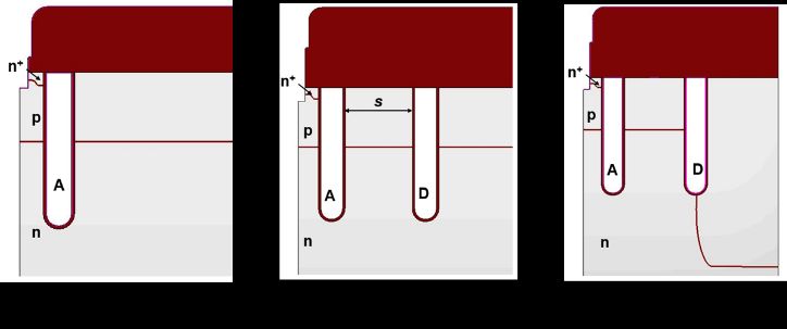
trench IGBT designs (Designs 1 - 3, Fig. 1) were
considered.                                                  Fig. 2: Plot showing the total time integrated
                                                                     avalanche generation near the active trench
                                                                     during the turn-off switching event for different
                                                                     designs.

                                                             Our novel ‘plasma flow control’ design plays an
                                                             important role in reducing avalanche generation by
                                                             another two orders of magnitude as can be seen in
                                                             Fig. 2. This is accomplished by diverting a
                                                             significant number of holes away from the active
Fig. 1: Schematic diagram of different IGBT protection       trench during the turn-off transient. In this situation,
        cell designs investigated using TCAD                 the dummy trench shares a significant part of the
        simulations.                                         avalanche generation as shown in Fig 3.

Design-1 consists of only an active (denoted by ‘A’)
trench (unprotected design), Design-2 features a                                                        1012                                           near active
                                                                       Time int. avalance gen. (cm-2)

                                                                                                                                                       near dummy
dummy trench (denoted by ‘D’) placed at a
distance s from the active. Design-3 consist of                                                         1011
additional deep p-well below the dummy trench. In
addition, the new ‘plasma flow control’ feature is                                                      1010
applied to Design-2 and Design-3 for the purposes
of investigating how dynamic avalanche is affected                                                      109
during turn-off. All other design paraments were
kept constant.                                                                                          108

                                                                                                        107
For this study, avalanche generation near the                                                                  without plasma flow control   with plasma flow control

active trench during the switching event was                                                                                         Design-3
explored as a measure of device degradation. As
can be seen in Fig. 2., in comparison to the
                                                             Fig. 3: Plot showing the avalanche generation at the
‘unprotected’ Design 1, the avalanche generation
                                                                     active and dummy trenches for Design-3 with
near the active trench is reduced by more than 2                     and without plasma flow control.
orders of magnitude for the proposed ‘protected”
Design 3. Design-3 with both dummy trench and p-
well is better protected against degradation as
compared to the other designs.

PCIM digital days 2021                                   2                                                      https://pcim.mesago.com/nuernberg/en.html
Avalanche generation near the active trench was
found to increase with increasing distance
between the dummy and active trenches (Fig. 4).                                                                                                             50          Design 1-no 'plasma flow control'
                                                                                                                                                                        Design 3-no 'plasma flow control'
Therefore, it is desired to place the dummy trench                                                                                                          45
                                                                                                                                                                        Design 3-'plasma flow control'
as close as possible to the active trench to protect                                                                                                        40
the latter from the impact of dynamic avalanche for                                                                                                         35

                                                                                                                                                Eoff (mJ)
better long-term stability and ruggedness.                                                                                                                  30
                                                                                                                                                            25
                                                                                                                                                            20

                                                                                                   Avalanche gen. ratio (Dummy/active)
                                                          Design-3
                                                                                              12                                                            15
  Time int. avalance gen. (cm-2)

                                                                                                                                                            10
                                   1013                                                       10                                                             5
                                                                                                                                                                 1.2   1.6     2.0    2.4      2.8      3.2
                                                       without plasma flow control (active)   8
                                   10   12
                                                       with plasma flow control (active)                                                                                      Vcesat (V)
                                                       with plasma flow control, D/A
                                                                                              6
                                   10   11                                                                                                   Fig. 5: Simulated technology curve (125 °C) for
                                                                                              4                                                      Design-1 and Design-3 (with and without
                                   1010
                                                                                                                                                     ‘plasma flow control’).
                                                                                              2

                                   109                                                        0
                                             0   1       2        3                  4
                                                     Spacing, s (mm)
                                                                                                                                             2.2 Device Performance
                                                                                                                                             Design-3      (“protected   design”)    was     also
                                                                                                                                             experimentally realized to verify the simulation
Fig. 4: Plot showing the avalanche generation near the                                                                                       findings. The p-well protecting the active trench
        active trench with varying spacing between the
                                                                                                                                             pair from degradation during repetitive switching
        dummy and active trenches for Design-3.
                                                                                                                                             events in Design-3, in this design is placed right
                                                                                                                                             next to the dummy trench. Like this, lateral dopant
                                                                                                                                             diffusion during processing annealing steps can be
Devices with the ‘plasma flow control’ feature,                                                                                              further stopped first by the dummy outer trenches
consistently show lower avalanche generation                                                                                                 guaranteeing that the p-well implant never merges
(Fig. 4 for Design-3) for all varied trench spacings.                                                                                        with the p-channel of the active trench. Such
Furthermore, an increasingly less percentage of                                                                                              design, when optimized and together with an
the avalanche generation is shared by the dummy                                                                                              excellent gate oxide quality, leads to a device with
trench when it is moved further away from the                                                                                                high blocking capability (> 1400 V) and stable
active trench.                                                                                                                               switching performance over time. It is minimally
                                                                                                                                             affected by the amount of dynamic avalanche
The proposed Design-3 has furthermore an added                                                                                               during hard switching applications as will be shown
advantage of reduced Miller capacitance [5]                                                                                                  later. It can be furthermore be manufactured with
thereby resulting in lower switching losses. It                                                                                              wide processing margins.
therefore also lies on a more favorable place in the
technology curve as shown in Fig. 5 (same Vce-sat                                                                                            Design-3 devices in different places in the
but lower Eoff) as compared to the unprotected                                                                                               technology trade-off curve (A, B, C, Fig. 6.
Design-1.                                                                                                                                    measured at Tj = 150 °C, 8.2 ohm, 150 nH), and
                                                                                                                                             hence different dynamic avalanche characteristics
                                                                                                                                             have been investigated. Different places in the
                                                                                                                                             technology curve could be achieved by simple
                                                                                                                                             changes in process parameters, such as anode
                                                                                                                                             doping or trench depth.

PCIM digital days 2021                                                                                                                   3                       https://pcim.mesago.com/nuernberg/en.html
29
                                                                                                   (reduced dV/dt) during voltage buildup points out
                                                                                                   to dynamic avalanche where the plasma sweep-
                28
                                                                                                   out rate is slowed down by the generation of new
                27
                                                                                    A              electron-hole pairs, slowing down the turn-off
                26                                                                  B              process [6].
                25                                                                  C
Eoff (mJ)

                24

                23                                                                                 3 Repetitive Switching
                22

                21
                                                                                                     Performance
                20                                                                                 The behavior and long-term stability performance
                19
                                                                                                   of the same devices was investigated under
                18
                                                                                                   dynamic repetitive stress conditions. Switching
                  1.6   1.8    2.0      2.2           2.4          2.6         2.8      3.0        was performed at 150 °C, which is the nominal
                                          Vce (V)                                                  junction temperature. The device in the field will be
                                                                                                   operated at high temperatures (≥ 125 °C) for a
Fig. 6: Technology trade-off curve measured at                                                     great majority of its lifetime. It is important to
        Vcc = 600 V,   Ic = 150 A   and   Tj = 150°C,                                              investigate device degradation under stress
        8.2 ohm, 150 nH. Devices A, B, C are                                                       conditions to be able to predict the lifetime of the
        experimentally realized variants of proposed                                               device and to be able to ensure its long-term
        Design-3.                                                                                  stability. For industrial applications with a lifetime
                                                                                                   of 15 years it’s estimated that devices would be
                                                                                                   exposed to approximately 1 million switching
Figure 7. Shows the turn-off waveforms measured                                                    events with twice the rated current [3]. In here
under reverse biased safe operating area                                                           devices were first switched 100 k times at 125 %
(RBSOA) conditions (300 A, 900 V, 8.2 ohm,                                                         Vnom = 750 V and 150 % Inom = 225 A conditions
150 nH, 150 °C) for different devices A, B and C.                                                  (150 A nominal rated current). Electrical
                                                                                                   parameters were extracted in an interval of 1000
                                                                                                   stress pulses.
            1200

            1000
  VCE (V)

               800

               600

               400                                                       A
                                                                         B                                           15000
               200                                                       C
                 0

               300

               250
     ICE (A)

               200                                                                                                   12000
               150

               100
                                                                                                      dV/dt [V/ms]

                50

                 0                                                                                                                                                   A
                15                                                                                                   9000
                                                                                                                                                                     B
                10
                                                                                                                                                                     C
      VGE (V)

                 5

                 0

                 -5
                                                                                                                     6000
                -10

                -15

                 4.50   4.75     5.00         5.25          5.50             5.75       6.00
                                          time (ms)
                                                                                                                     3000
                                                                                                                             0       20000   40000   60000   80000       100000

Fig. 7: RBSOA turn-off waveforms measured at                                                                                                 Burst Number
        Vcc = 900 V, Ic = 300 A and Tj = 150 °C,
        8.2 ohm, 150 nH.
                                                                                                   Fig. 8: Evolution of dV/dt measured under nominal
                                                                                                           conditions. The devices are switched 100 k
                                                                                                           times at 1.25 x Vnom and 1.5 x Inom.
Strong avalanche can be observed in all tested
devices but specially on device C. Dynamic
avalanche happens when IGBTs are switched at
high currents with high dV/dts and can be identified
from the voltage turn-off switching waveform. The
curvature in the voltage turn-off waveform

PCIM digital days 2021                                                                         4                                 https://pcim.mesago.com/nuernberg/en.html
Figure 8 shows the No significant change in the
static and switching behavior was found after 100 k
                                                                                                            600

                                                                                                                     device B

                                                                                                 VCE (V)
switching pulses for the different devices                                                                  400

regardless     of    their  dynamic     avalanche                                                           200

characteristics.                                                                                              0
                                                                                                            300

                                                                                                                                       Initial

                                                                                                  ICE (A)
                                                                                                            200

Since no degradation was observed after 100k                                                                                           after 50k pulses
                                                                                                                                       after 100k pulses
pulses at 1.5 x Inom, the test was repeated                                                                 100

at 4 x Inom (600 A) for devices B and C. The higher                                                           0
                                                                                                             15

current level should drastically increase avalanche                                                          10

                                                                                                   VGE (V)
generation, therefore speeding up degradation.                                                                5

                                                                                                              0

Figure 9 and 10 show the turn-off and turn-on                                                                 -5

waveforms before and after 50 k and 100 k
                                                                                                             -10

                                                                                                             -15

switching pulses measured under nominal                                                                       4.75              5.00                5.25

                                                                                                                                                           time (ms)
                                                                                                                                                                       5.50   5.75   6.00

conditions (150 A, 600 V) for device B and Figure
10 and 11 respectively for device C.                                                            Fig. 10: Turn-on waveforms for device B measured at
                                                                                                         Vcc = 600 V, Ic = 150 A and Tj = 150 °C,
                                                                                                         8.2 ohm, 120 nH before and after 50 k and
            800

                     device B
                                                                                                         100 k pulses. The devices are switched 100 k
            600
                                                                                                         times at 1.25 x Vnom and 4 x Inom.
 VCE (V)

            400

            200

              0

            150
                                                                                                            800
                                                                 Initial
                                                                                                                     device C
  ICE (A)

            100                                                  after 50k pulses                           600
                                                                                                 VCE (V)

                                                                 after 100k pulses
             50                                                                                             400

                                                                                                            200
              0

             15
                                                                                                              0
             10
   VGE (V)

                                                                                                            150
              5

              0                                                                                                           Initial
                                                                                                  ICE (A)

                                                                                                            100
              -5                                                                                                          after 50k pulses
             -10                                                                                                          after 100k pulses
                                                                                                             50
             -15

              4.75              5.00   5.25               5.50              5.75     6.00
                                                                                                              0
                                              time (ms)                                                      15

                                                                                                             10
                                                                                                   VGE (V)

                                                                                                              5

Fig. 9: Turn-off waveforms for device B measured at                                                           0

        Vcc = 600 V, Ic = 150 A and Tj = 150 °C,                                                              -5

                                                                                                             -10

        8.2 ohm, 120 nH before and after 50 k and                                                            -15

                                                                                                              4.75              5.00                5.25               5.50   5.75   6.00
        100 k pulses. The devices are switched 100 k                                                                                                       time (ms)
        times at 1.25 x Vnom and 4 x Inom.
                                                                                                Fig. 11: Turn-off waveforms for device C measured at
                                                                                                         Vcc = 600 V, Ic = 150 A and Tj = 150 °C,
                                                                                                         8.2 ohm, 120 nH before and after 50 k and
                                                                                                         100 k pulses. The devices are switched 100 k
                                                                                                         times at 1.25 x Vnom and 4 x Inom.

PCIM digital days 2021                                                                      5                               https://pcim.mesago.com/nuernberg/en.html
600

                     device C
 VCE (V)

            400

                                                                                                           6000
            200

              0

            400                                                                                            5000

            300
                        Initial
  ICE (A)

                        after 50k pulses
            200         after 100k pulses
                                                                                                           4000

                                                                                            dI/dt [A/ms]
            100

              0
             15
                                                                                                           3000
             10                                                                                                                                    B
   VGE (V)

              5                                                                                                                                    C
              0

              -5                                                                                           2000
             -10

             -15

              4.75              5.00        5.25               5.50   5.75   6.00
                                                                                                           1000
                                                   time (ms)                                                      0       20000   40000    60000   80000       100000
                                                                                                                                  Burst Number
Fig. 12: Turn-on waveforms for device C measured at
         Vcc = 600 V, Ic = 150 A and Tj = 150 °C,
         8.2 ohm, 120 nH before and after 50 k and                                      Fig. 13: dI/dt evolution measured under nominal
         100 k pulses. The devices are switched 100 k                                            conditions for devices B and C. The devices are
         times at 1.25 x Vnom and 4 x Inom.                                                      switched 100 k times at 1.25 x Vnom and 4 x Inom.

The turn-on and off delay time td for device C with
stronger dynamic avalanche characteristics                                                                  450
changes only slightly over time as. An increase in
delay time does indicate nonetheless that                                                                   425

positively charged interface traps form at the
Si/Oxide interface [1]. The positively charged traps                                                        400

increase the td and slow down the devices.
                                                                                              IC,max [A]

                                                                                                            375
                                                                                                                                                           B
                                                                                                                                                           C
                                                                                                            350

Charge trapping and oxide degradation can also                                                              325
be manifested in changes in the turn-on dI/dt and
turn-off dV/dt. The carrier density concentration                                                           300

near the trench bottom varies depending on the
                                                                                                            275
plasma concentration. Devices with strong                                                                         0       20000   40000    60000   80000       100000

dynamic avalanche are expected to degrade the                                                                                      Burst Number
most over time at this point. Two characteristics
serve to stop device degradation under certain
conditions: the superior quality of the gate oxide                                      Fig. 14: Ic,max evolution measured under nominal
                                                                                                 conditions for devices B and C. The devices are
that does not allow for a high number of energetic
                                                                                                 switched 100 k times at 1.25 x Vnom and 4 x Inom.
carriers to be injected and trapped and the device
design. The use of dummy trenches on the sides
of the active trench pair serve to stop the extension
of the p-well and merge with the channel. Even
though avalanche generation increases hole
injection significantly, the active trench seems to
be protected enough as to not cause significant
damage over time. Figure 13, 14 and 15 shows the
dI/dt, Ic,max and Eon evolution respectively
measured under nominal conditions (devices are
switched 100k times at 1.25 x Vnom and
4 x Inom).The strongest deviation of less than 5 %
and 10 % was in fact found for device C on the Eon
and Ic,max respectively.

PCIM digital days 2021                                                              6                                 https://pcim.mesago.com/nuernberg/en.html
conditions when strong dynamic avalanche is
                30                                                    present. The combination of above elements
                                                                      (dummy trench, p-well, ‘plasma flow control’) in
                25                                                    Design-3 provides a robust design against
                                                                      repetitive RBSOA turn-off pulses and switching
                20                                                    losses.
     Eon [mJ]

                15

                                                         B            5 References:
                10                                       C
                                                                      [1] J. Lutz, R. Baburske: Dynamic avalanche in
                5                                                         bipolar devices, Microelectronics Reliability 52,
                                                                          2012, 475-481.
                0
                     0   20000   40000   60000   80000   100000       [2] T. Laska, F. Hille, F. Pfirsch, R. Jereb, M. Bassler:
                                 Burst Number                             Long Term Stability and Drift Phenomena of
                                                                          different Trench IGBT Structures under Repetitive
                                                                          Switching Tests, Proc. ISPSD, 2007, 1-4.
Fig. 15: Eon evolution measured under nominal
                                                                      [3] C. Sandow, P. Brandt, H.-P. Felsl, F.-J.
         conditions for devices B and C. The devices are
                                                                          Niedernostheide, F. Pfirsch, H. Schulze, A.
         switched 100 k times at 1.25 x Vnom and 4 x Inom.
                                                                          Stegner, F. Umbach, F. Santos, et al.: IGBT with
                                                                          superior long-term switching behavior by
                                                                          asymmetric trench oxide, ISPSD, 2018, 24-27.
4 Conclusion                                                          [4] C. E. Blat: Mechanism of negative‐bias‐
In here we have presented the next generation FP                          temperature instability, Journal of Applied Physics
trench IGBT from Hitachi ABB Power Grids. The                             69, issue 3, P1712-1720, 1991.
new and optimized design is capable of long term                      [5] M. Sawada, K. Ohi, Y. Ikura, Y. Onozawa, M.
and rugged performance regardless of whether the                          Otsuki, Y. Nabetani: Trench shielded gate concept
device has strong dynamic avalanche when                                  for improved switching performance with the low
switched under hard conditions at 1.5 x Inom. It                          Miller capacitance, ISPSD, 2016, 207-210.
furthermore minimally degrades at 4 x Inom

PCIM digital days 2021                                            7              https://pcim.mesago.com/nuernberg/en.html
You can also read