Magnetic tunnel junctions and magnetic logic circuits driven by spin-orbit torques - Uni Mainz
←
→
Page content transcription
If your browser does not render page correctly, please read the page content below
Magnetic tunnel junctions and magnetic logic circuits
 driven by spin-orbit torques

 P. Gambardella
 Department of Materials, ETH Zürich, Switzerland

 E. Grimaldi K. Garello Z. Luo
 V. Krizakova F. Yasin A. Hrabec
 P. Dao S. Couet A. Kleibert
 L. Heyderman
 A. Hrabec G.S. Kar
 M. Wörnle
 S. Velez
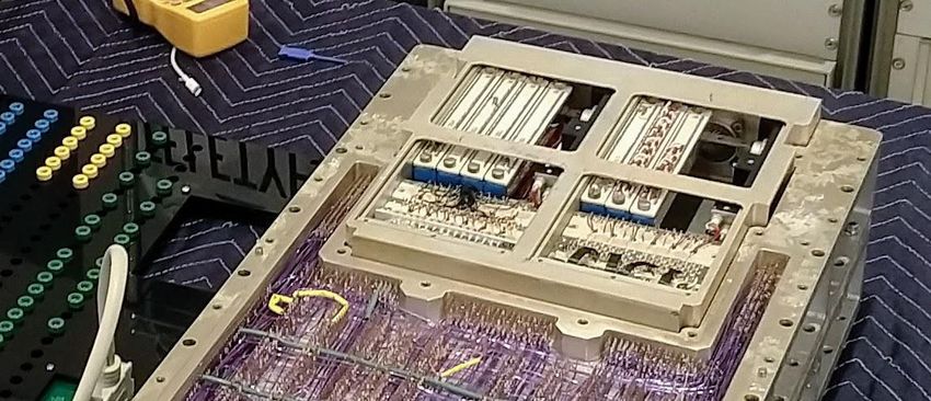
The Apollo Guidance Computer

Images from NASA and Wikipedia
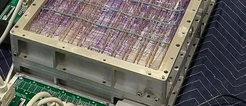
The magnetic core memory Magnetic‐core memory was the predominant form of random‐ access computer memory between 1955 and 1975. It was used in the Apollo Guidance Computer and Space Shuttle IBM flight computers until 1990. Non‐volatile Clock rate of ∼1 MHz. 32 kilobits per cubic foot 1 cent per bit.

The magnetic core memory

 WRITE

 READ
A modern magnetic random access memory

 Chappert, Fert & Van Dau, Nat. Mater. 2007
Need for fast & nonvolatile memories

 On‐chip CPU
 (embedded) Register
 SOT‐MRAM
 0.5 ‐ 5ns

 CPU CACHE
 Levels 1 & 2 SRAM STT‐MRAM: eMRAM
 Levels 3 & 4 eDRAM 5 ‐ 100ns
 DENSITY
SPEED

 MAIN MEMORY
 RAM DRAM dense STT‐MRAM

 Off‐chip
 (stand‐ SOLID STATE MEMORY
 alone) NAND
 NON‐VOLATILE MEMORY FLASH

 VIRTUAL MEMORY

 MAGNETIC HARD DRIVES & TAPES
Beyond‐CMOS electronics

 Salahuddin and Datta, Nat. Electr. 1, 442 (2018)
Interconversion of linear momentum, angular momentum & …

 S
 L

 k
The spin Hall effect

 Spin‐dependent scattering gives rise to
 transverse spin imbalance

 j

 Dyakonov and Perel, JETP Lett. 13, 467 (1971)
 Kato et al., Science 306, 1910 (2004)
 Wunderlich, Phys. Rev. Lett. 94, 047204 (2005)
 Sinova et al., Rev. Mod. Phys. 87, 1213 (2015)

 Pt 0.05 0.2
 Pt 1 14
The Rashba-Edelstein effect

 + + + + +
 + + + + +
INTERFACE
 ‐ ‐ ‐ ‐ ‐
 ‐ ‐ ‐ ‐ ‐

 Electrons move in an uncompensated ‐field: ∼ ~

 ∗

 2 ℏ

 The Rashba field induces a homogenous in‐plane spin polarization

 Edelstein, Solid State Commun. 1990; Manchon Nat. Mater. 2015; PG and Miron, Phil. Trans. R. Soc. 2011
Current induced spin‐orbit torques in FM/NM bilayers

 Spin Hall effect Rashba‐Edelstein effect
 Interface spin Hall effect
 Spin‐dependent scattering

 Manchon et al., Rev. Mod. Phys. 91, 035004 (2019)
Spin‐orbit torque induced switching of a single ferromagnetic layer 1 I AlOx Co Pt 0 Transfer of orbital to spin momentum Mx > 0 Efficient spin injection/No polarizer Compatible with PMA Mx < 0 Scalable CMOS compatible Three‐terminal devices Miron et al., Nature 476, 189 (2011)
Current‐induced domain wall motion in Pt/TmIG: expansion

 p‐MOKE
 = 108 A cm‐2
 = 250 ns
 = 215 Oe

 Vélez et al.,
 Nat. Comm. 10,
 4750 (2019)
Spin-orbitronics
 Functionalities & applications
Magnetization switching High-frequency oscillations Domain wall and skyrmion motion Spin-wave excitations

 V

 Magnetic memories GHz and THz nanooscillators Race-track memories Chargeless interconnect
 & spin logic

 Materials
 Magnetic metallic Magnetic Insulators Non-centrosymmetric magnets Antiferromagnets
 heterostructures (YIG, TmIG, Bi:YIG…) (Ga,Mn)As, MnNiSb… (CuMnAs, NiO, IrMn…)

 Co, Ni, Fe, GdFeCo...
 Pt, W, Ta…
 WOx, CuOx , SrIrO3...
 Bi2Se3, WTe2, MoS2...

 Manchon, PG et al., Rev. Mod. Phys. 91, 035004 (2019)
Two‐terminal vs three‐terminal MTJs

 STT‐MTJ Perpendicular SOT‐MTJ
Three‐terminal spin‐orbit torque MTJs

 Perpendicular MTJ In-plane MTJ In-plane MTJ
 “y-Type” “x-Type”

 Cubukcu et al., Liu et al., Fukami et al.,
APL 104, 042406 (2014) Science 336, 555 (2012) Nat. Nano. 11, 621 (2016)
Three terminals are more than two

 Voltage‐assisted SOT switching of
 MTJs on a self‐aligned Ta‐B SOT STT + SOT switching at zero field
 electrode

 Kato et al., Phys. Rev. Appl. 10, 044011 (2018)
 Wang et al., Nat. Electron. 1, 582 (2018)
STT vs SOT magnetization dynamics

 STT ‐ MTJ SOT ‐ MTJ

 M2

 M1 I

 M
 Torque
 Torque

 M

 • Delayed • Instantaneous
Fast and reliable switching of SOT‐MTJs

 12
 J (10 A/m2)
 (a) -4.5 -3 0 3 4.5
 60

 40
 TMR (%)

 550
 20

 0
 10
 -40 -20 0 20 40
 I (mA)
 P

 Cubukcu et al., IEEE TM 54, 9300204 (2018) Aradhya et al., Nano Lett. 16, 5987 (2016)
 Cubukcu et al., APL 104, 042406 (2014)
Time‐resolved measurements of 3‐terminal MTJs
driven by SOT, STT, VCMA

Imec ‐ Interuniversity Microelectronics Centre, Leuwen, Belgium
K. Garello, F. Yasin, S. Couet, G.S. Kar

ETH Zurich
E. Grimaldi, V. Krizakova, G. Sala, PG
Three‐terminal SOT‐MTJ 8 STT electrode RAP 6 RMTJ (k) MTJ p-SAF SOT output CoFeB 4 electrode electrode MgO CoFeB RP W W line 2 200 nm 10 nm -200 -100 0 100 200 0Hz (mT) v1 Vdc z V1 x Samples fabricated at VSTT scope V0 VSOT Vout v0 E. Grimaldi, V. Krizakova, K. Garello, PG et al., Nat. Nanotech. 15, 111 (2020)
Bias voltages in a three‐terminal SOT‐MTJ

 1
 2 4

 Assuming ≪

 0.5

 v1 Vdc
 1.09 0.46
V1

 VSTT scope

V0
 VSOT Vout
 v0

 E. Grimaldi, V. Krizakova, K. Garello, PG et al., Nat. Nanotech. 15, 111 (2020)
After‐pulse switching probability Vdc read STT Vrf SOT SOT RT MR () 6 RAP STT 4 RP 0 50 100 Events (count s) E. Grimaldi, V. Krizakova, K. Garello, PG et al., Nat. Nanotech. 15, 111 (2020)
Single‐shot measurements of SOT switching in a 3T‐MTJ STT only SOT ‐ STT SOT + STT (VCMA) SOT + STT (VCMA) + field 0 0.45 0.45 0.45 0.88 V =0.23 -227 mV V 0.27 mV = +513 0.51 STT STT 0 mT -23 mT -23 mT t -90 mT t0 0 5 10 0 5 10 0 5 10 0 5 10 Time (ns) Time (ns) Time (ns) Time (ns) E. Grimaldi, V. Krizakova, K. Garello, PG et al., Nat. Nanotech. 15, 111 (2020)
Analysis of single‐shot SOT switching events at low in‐plane field 2 Vsw (norm.) 1 t0 0 t -1 0 5 10 Time (ns) Incubation Reversal Total switching time + =
Analysis of single‐shot SOT switching events at large in‐plane field 2 Vsw (norm.) 1 t0 0 t -1 0 5 10 Δ 0.9 0.16 Time (ns) Incubation Reversal Total switching time + =
Origin of the incubation and reversal time in SOT switching 400 1 Pulse T (K) 350 300 800 Aex (pJ m-1) MS (MA m-1) K (kJ m-3) . 650 Mz (norm.) 500 0Hx (mT): 0Hx (m 0 1.1 35 45 45 60 1 60 70 0.9 70 90 90 15 . 12 9 -1 0 2 4 6 8 10 12 14 0 2 4 6 8 10 0 Time (ns) Time (ns) T E. Grimaldi, V. Krizakova, K. Garello, PG et al., Nat. Nanotech. 15, 111 (2020) Baumgartner et al., Nat. Nanotech. 12, 980 (2017)
Separating the effects of STT and VCMA (voltage control of magnetic anistropy) VSTT/VSOT 1 1.0 VSTT -0.5 Vsw (norm.) +0.6 vc (norm.) Critical SOT switching V (mV) vc +1.1 SOT STT voltage vs ratio -197 STT 0.8 vc +73 0 +232 reference: up VSOT +447 down 0.6 Hx 0 10 20 0 1 2 3 4 5 Time (ns) 1/p (ns-1) 0.8 VSTT/VSOT 1.0 0.27 ns VCMA: VSTT -0.5 20 ns vc 0.6 0.0 +0.6 0.8 ̅ ↑ ↓ /2 Vc (V) +1.1 0.4 SOT STT 0.2 0.0 STT: vc 0.27 ns VSOT -0.2 20 ns Δ ↑ ↓ ⁄2 0.0 0 5 10 15 20 0 1 p (ns) VSTT/VSOT E. Grimaldi, V. Krizakova, K. Garello, PG et al., Nat. Nanotech. 15, 111 (2020)
Field‐free SOT switching of a 3‐terminal MTJ below 1 ns

 0

 V. Krizakova, K. Garello, PG et al.,
 Appl. Phys. Lett. 116, 232406 (2020)
 Garello et al.,
 IEEE Symp. VLSI Technol., T194 (2019)
SOT vs STT switching: speed and efficiency
 STT is more efficient than STT at large 5
 SOT reaches maximum efficiency at 1
 SOT‐only:
 ≈ 100 % switching probability
 @ 0.3 ns /

 AP-P
 = 0.27 ns
 P-AP

 critical E (pJ)
 10

 SOT
 1

 STT
 0.1
 0.1 1 10
 Pulse length (ns)
 +997 mV
 / 0.5 , 0.4 V
 +23 mT , 2.0 10 A cm‐2
 , 0.75 V
 , 4.2 10 A cm‐2

 E. Grimaldi, V. Krizakova, K. Garello, PG et al., Nat. Nanotech. 15, 111 (2020)
SOT‐MRAMs: figures of merit Cell size (cost): > STT, < SRAM Downscale the MTJ and SOT current line Write energy: > STT Increase the STT bias. Write speed: > STT Exploit the VCMA effect. Read speed: > STT at equal RDR Increase the SOT efficiency Endurance: > STT at high speed CMOS compatibility: ok 10 80 nm MTJ: SOT data VSTT/VSOT = +1.1 1 Ic (mA) 30 nm MTJ: SOT 0.1 VSTT/VSOT = +3.6 extrapolation VCMA = 120 fJ V-1 m-1 1 0.01 0.1 1 10 p (ns) E. Grimaldi, V. Krizakova, K. Garello, PG et al., Nat. Nanotech. 15, 111 (2020)
Conclusions #1 Single‐shot dynamics driven by SOT in 3‐terminal MTJs SOT incubation time due to strong anisotropy preventing domain nucleation Interplay of SOT, STT, VCMA, and Joule heating Extremely narrow switching time distributions can be achieved (std < 0.16 ns) ≈ 100% SOT switching rate at 0.3 ns at 2 Sub‐ns field‐free SOT switching with MTJ hard magnetic mask SOT becomes energy‐competitive below 1 ns Strategies to improve SOT efficiency Grimaldi et al., Nat. Nanotech. 15, 111 (2020) Krizakova et al., Appl. Phys. Lett. 116, 232406 (2020)
Magnetic logic circuits driven by spin‐orbit torques

ETH Zürich & Paul Scherrer Institute
Lab for Mesoscopic system:
Zhaochu Luo, Aleš Hrabec, Eugenie Kirk,
Jizhai Cui, Anja Weber, Sina Mayr,
Laura Heyderman

Lab for Magnetism and Interface Physics: Phuong Dao, Manuel Baumgartner,
Gunasheel Krishnaswamy, Giacomo Sala, Junxiao Feng, Pietro Gambardella

Paul Scherrer Institute
Swiss Light Source: Jaianth Vijayakumar, Tatiana Savchenko, Simone Finizio,
Armin Kleibert, Jörg Raabe
Lab for Micro &Nanotechnology: Vitaliy Guzenko
Proposals for spin‐based logic devices

 Spin transistor MRAM‐based logic‐in‐memory
 RHigh = ‘0’
 RLow = ‘1’

 S.Datta et al. APL (1990) T. Hanyu et al. Proc. IEEE (2016)

 Nanomagnet logic Magnetic domain‐wall logic

 N S
 ‘0’ ‘0’

 S N
 ‘1’
 ‘1’
 A.Imre et al. Nature (2006) D.Allwood et al. Science (2005)
SOT‐driven magnetic domain walls

 High speed Interplay of DMI and SOT
 Chirality control and
 positioning of DW

 Thiaville et al., Europhys. Lett. 2012
 Emori et al., Nat. Mater. 2013
 Miron et al., Nat. Mater. 2011
 Cai et al., Nat. Electr. 2020
 SOT + exchange
 Depinning coupling torque

 Franken et al., Sci. Rep. 2014
 Chen et al., Nat. Comm. 2013
 Yang, Ryu &Parkin, Nat. Nano. 2015
Haazen et al., Nat. Mater. 2013
Advantages of magnetic DW logic
 • Complete set of logic elements → arbitrary logic circuit
 • Same objects for logic inputs and outputs → easy cascade
 • Logic gate defined by geometric structure → flexible design
 • Emerging current‐driven domain‐wall memory devices

 Manfrini et al. AIP Adv. (2018)
Parkin & Yang, Nature Nano. 2015 Zhao et al., IEEE Trans. Mag. 2011
 Chang et al., IEEE J. Expl. Sol. State Comp. Dev. 2016
 …
Implementing basic logic gates is not always straightforward…

 NOT gate

 H‐H DW

 D.Allwood et al. Science (2002)
From chiral Néel walls to chirally‐coupled nanomagnets
Control of magnetic anisotropy by selective oxidation of Pt/Co/Al

 Pt(6 nm)/Co(1.6 nm)/Al (2 nm)
 Pt(6 nm)/Co(1.6 nm)/AlOx (2 nm)
 IP CONTROL OF MAGNETIC
 ANISOTROPY

 Oxidation
 Monso et al., Appl. Phys. Lett. 2002
 Rodmacq et al., Phys. Rev. B 2009

 Ion irradiation
 Fassbender et al., J. Phys. D 2004
OOP Haazen, Nat. Mat. 2013

 Gating
 Ta Weisheit et al., Science 2007
 AlOx Al Maruyama et al., Nat. Nano. 2009
 Co Bauer et al., Nat. Mater 2013
 Pt
Dao et al., Nano Lett. 19, 5930 (2019)
Chirally coupled OOP and IP nanomagnets

 XPEEM @ SIM beamline/PSI

 Luo, Dao, Hrabec, Heyderman, PG et al., Science 363, 1435 (2019)
Lateral exchange bias induced by chiral coupling

 Luo, Dao, Hrabec, Heyderman, PG et al., Science 363, 1435 (2019)
Field‐free spin‐orbit torque switching of chirally coupled
nanomagnets

 Luo, Dao, Hrabec, Heyderman, PG et al., Science 363, 1435 (2019)
artificial spin ices
 synthetic skyrmions

 planar synthetic
 antiferromagnets

 chiral coupling field‐free
 SOT switching
 Z. Luo et al.,
 Science 363, 1435 (2019).
 domain wall
 T.P. Dao et al.,
 injector
lateral exchange bias Nano Lett. 19, 5930 (2019).
Current‐driven domain‐wall inverter STXM measurement of an
 OOP‐IP‐OOP racetrack

 J

 Experimental
 J

 realization

 J

 J

 The ⨂|⨀ DW is inverted into
Z. Luo, et al., Nature 579, 214 (2020). a ⨀|⨂ DW by the current pulses
Current‐driven domain‐wall inversion process

 Luo, Hrabec, et al., Nature 579, 214 (2020) Dao et al., Nano Lett. 19, 5930 (2019)
Nucleation of the V‐shaped IP region provides a well
 reversed domains defined nucleation center

 J

 Initial
operation
 2nd

 J x2
operation
 3rd

 J x4
operation
 4th

 J x6
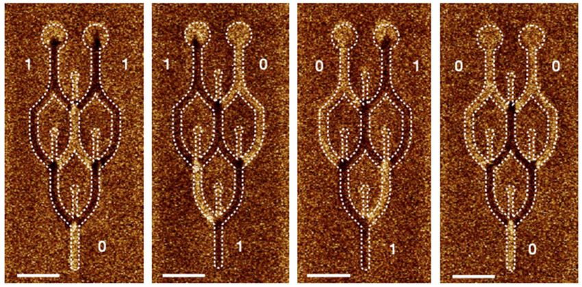
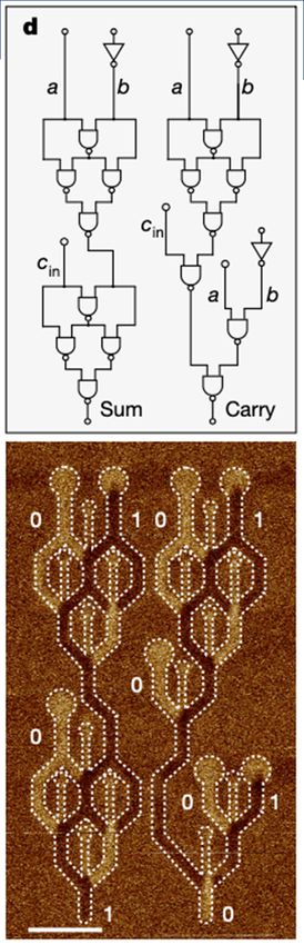
Domain‐wall NOT gate
 We define ⊗ = logical ‘1’ and ⊙ = logical ‘0’
 Input Output
 Input Output =
 Data flow Cascaded NOT gates
 ⊙|⊗|⊙

 initial

 x6

 x2 x9
 ⊗|⊙|⊗
 x14
 x5
Current Bias
 Input a Input b
 DW reservoir w/wo
 inverter to define Bias
 inputs Input a Input b

 Computation core
 based on chiral 200 nm
 coupling

 0 0 0 0
 1 1
NAND

 1 0 0 1 0 0
 0 1 1 1

 1 1 1 1
 0 1
NOR

 1 1 1 0 0 0

 0 0 0 1
Current‐driven operation of a NAND gate with a sequence of logic inputs

 1 1 1
 0 0 input a
 1 1 1
 1 1 1 output 0 0
 0 0 input b

 Luo, Hrabec, et al., Nature 579, 214 (2020)
A complete set
of logic
elements

Luo, Hrabec, et al.,
Nature 579, 214 (2020)
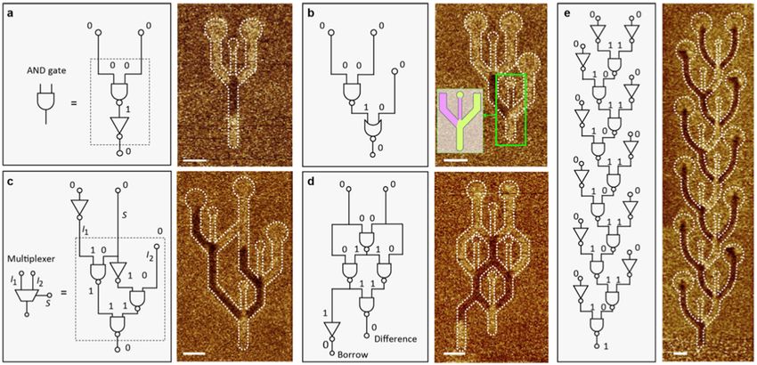
Examples of DW logic circuits #1

 AND gate NAND+NOR circuit

 2‐bit multiplexer Half subtractor Long circuit

 Luo, Hrabec, et al., Nature 579, 214 (2020)
Examples of DW logic circuits #2

 Full adder
Half adder
Propagation delay time for DW motion

• Asynchronized DW motion
• Need for delay time
Issues to be addressed in the future

 Scaling down vs performances
 800 nm‐wide
 Electrode

 Electrode
 Pinning
 DW inverter
 DW speed
 ~150 m/s
 Synchronization
 ⊙|⊗ initial

 Integration Feedback loops
 Input

 Input
 Bias
 MTJ

 MTJ
 MTJ Output

 NAND MTJ
 gate
Conclusions #2 DMI enables flexible design of synthetic chiral magnets Field‐free switching in OOP‐IP coupled magnets +Hz SOT DW injectors Current‐driven DW inverter Electrode Electrode Reconfigurable NAND/NOR gate ⊙|⊗ initial Logic operations with DWs in cascaded logic circuits Z. Luo, et al., Science 363, 1435 (2019). T.P. Dao, et al., Nano Lett. 19, 5930 (2019). Z. Luo, et al., Nature 579, 214 (2020). Z. Luo, et al., EU patent EP20161352.8.
You can also read