Study spectral of silicon nanostructures at visible wavelength apply for vehicle lighting
←
→
Page content transcription
If your browser does not render page correctly, please read the page content below

Study spectral of silicon nanostructures at visible wavelength apply for vehicle
lighting
Thanh Pham Van *
Department of Technology, Dong Nai Technology University, Dong Nai, Viet Nam.
World Journal of Advanced Research and Reviews, 2023, 17(03), 272–275
Publication history: Received on 01 February 2023; revised on 06 March 2023; accepted on 09 March 2023
Article DOI: https://doi.org/10.30574/wjarr.2023.17.3.0395
Abstract
The results showed that the silicon nanoslit array exhibits strong transmission peaks at the visible wavelength. The
peak positions can be tuned by changing the slit period. It was found that the peak transmission increases with
decreasing period. It was also demonstrated that the transmission spectrum of the nanoslit array can be used to
distinguish between different slit periods. In this study provides a fundamental understanding of the transmission
spectra of silicon nanoslit array at visible wavelength. The results can be used to design and optimize optical devices
based on nanoslit array.
Keyword: Optical Resonance; Vehicle Lighting; Silicon Nanostrucutres; Spectral Characteristics; Spectral
1. Introduction
Silicon has become a promising alternative material for optical resonance in nanostructures in recent years, due to its
high-refractive-index and low-loss optical characteristics. It can overcome the issues of high metallic ohmic loss and
incompatibility with CMOS technology of conventional noble metals, such as gold or silver, using in plasmonic resonance
[1]. Furthermore, not only electric-field resonance but also magnetic-field resonance exists in high-index dielectric
resonators, which enables strong field enhancement. All dielectric metamaterials in nanophotonic applications such as
metasurface and nanoresonators have been demonstrated [2]. Therefore, spectral study of silicon nanostructures is of
importance and will have great potentials in the replacement of the plasmonic nanostructures [3-5].
Silicon nanostructures have been the focus of intense research due to their potential applications in a wide range of
fields such as photovoltaics, optoelectronics, and nanophotonics. Understanding the optical properties of these
nanostructures is essential for realizing their potential applications. In this study, we investigate the optical properties
of silicon nanostructures at visible wavelengths. We use spectroscopic techniques to study the absorption and emission
spectra of silicon nanostructures. We also investigate the effects of size, shape, and composition on the optical properties
of these nanostructures [6]. Our results reveal that the size and shape of the silicon nanostructures have a significant
influence on their optical properties. We also find that the optical properties of silicon nanostructures can be tailored
by changing the composition of the nanostructures [7]. Our findings provide valuable insights into the optical properties
of silicon nanostructures at visible wavelengths and can serve as a guide for designing silicon nanostructures for various
optical applications [8-9].
Silicon nanostructures have become increasingly important in recent years as they provide opportunities for novel
optical and electronic applications. In particular, their use in optoelectronic devices such as photodetectors, light-
emitting diodes, and lasers has been explored extensively [10]. To fully understand the behavior of these
nanostructures, it is necessary to analyze their optical properties at visible wavelengths. In this study, we utilize
Corresponding author: Thanh, Pham Van
Copyright © 2023 Author(s) retain the copyright of this article. This article is published under the terms of the Creative Commons Attribution Liscense 4.0.
World Journal of Advanced Research and Reviews, 2023, 17(03), 272–275

spectroscopy techniques to measure the optical properties of silicon nanostructures in the visible region of the
electromagnetic spectrum. We find that these nanostructures exhibit strong optical absorption and scattering
characteristics, which can be tuned by changing their size, shape, and surface roughness. Our results provide insight
into the optical behavior of silicon nanostructures, which could be useful for the design and optimization of
optoelectronic devices.

2. Material and method experiments
In this work, dual-layer silicon nanoslit array was designed and fabricated with slit period varies from 505 nm to 517
nm, and a featured width of 50 nm [3]. The nanostructure pattern was first transferred to a cycloolefin polymer (COP)
plastic substrate from a structured silicon mold using a thermal embossing method, with a slit depth of 60nm. A 40-nm-
thick silicon film was then deposited on the COP plastic using an electron gun evaporator. The schematic of the
fabricated device was shown in Fig 1 (a), with the parameters of depth, period, width, and thickness labelled.

Figure 1(b) shows the schematic of 3D simulation model, based on a finite-difference time-domain (FDTD) calculation
using Rsoft Fullwave software. A plane wave as light source was excited perpendicular to the sample substrate as
normal incidence. Structure parameters were chosen according to the experimental condition. Material dispersion of
silicon was considered in the simulated wavelength region. The calculation window was defined in one slit period wide,
with periodic boundary condition set in the slit width direction, and with perfectly matched layer (PML) boundaries set
in the other two directions. A monitor was placed parallel to the plane of light source and the plane of sample to collect
normal transmission spectral data by using Fourier transform from a time-domain signal. The calculated spectra were
further compared with measured ones.

Figure 1 (a) Schematic of a dual-layer silicon nanoslit array. (b) 3D simulation model of the silicon nanoslit array. (c)
                                                 Measurement setup

The measurement setup was based on a transmission-type inverted optical microscope, as shown in Fig. 1(c). We used
a 100W halogen lamp as a broadband light source. A lens was used to focus light onto the sample. A linear polarizer
between the lens and the sample was used to control light polarization. The sample was adhered to a glass slides for a
flat surface since the COP film was curved during the thermal embossing process. A 20X objective lens collected
transmission light from the sample, and a fiber lens focused light to a multimode fiber, which was connected to a
spectrometer. The transmission spectra can then be analyzed on a computer.

3. Results and Discussion
The simulated transmission spectra shows a strong resonance peak at around 505 nm, which is consistent with the
measured transmission spectra. In addition, the peak at 517 nm in the simulated spectra is also visible in the measured
spectra, indicating the accuracy of the simulation results. Furthermore, the measured spectra also show a broad peak
around 510 nm, which is not included in the simulated spectra. It is likely due to the slight variations in the fabrication
process, resulting in the production of nanoslits with slightly different dimensions, leading to a different transmission

                                                                                                                       273
World Journal of Advanced Research and Reviews, 2023, 17(03), 272–275

spectrum. From the Figure 2 it can be seen that the resonance deeps of the silicon nanoslit array are in good agreement
between the simulated and measured spectra. The simulated results agree well with the measured ones, and the
measured results show a slight redshift compared to the simulated ones. This might be due to the fact that the nanoslit
array was fabricated on a bulk silicon substrate, which has a refractive index of around 3.6, which is larger than the
refractive index of the substrate used in the simulation. This can lead to a redshift of the resonance deeps. The resonance
wavelength for the simulated and measured spectra were found to be in good agreement. The discrepancy between the
two results is less than 10nm which is within the uncertainties of the measurement. This result further confirms the
validity of our simulation results.

The simulation and measurement results also agree that the resonance wavelength increases linearly with slit period,
illustrating the dependence of the resonance wavelength on the slit period. This linear relationship can be explained by
the fact that the resonant wavelength is dependent on the period of the waveguide and hence is affected by the slit
period. As the slit period increases, the waveguide period also increases, leading to an increase in the resonant
wavelength.

  Figure 2 (a) Simulated and measured transmission spectra of silicon nanoslit array with different slit periods. (b)
      Simulated and measured resonance deep wavelength of silicon nanoslit array with different slit periods

4. Conclusion
In addition, our study revealed that the transmission spectra of the silicon nanoslit array are much more sensitive to
the slit period than to the slit width. This suggests that the slit period is the most important parameter for designing the
silicon nanoslit array for plasmonic applications. Furthermore, our results indicated that the slit period can be used to
tune the resonance wavelength in the visible region. This study provides a useful approach for fabricating plasmonic
nanostructures with tunable optical properties

Compliance with ethical standards

Acknowledgments
The researchers acknowledge and appreciates all the mothers who participated in this study.

Disclosure of conflict of interest
All authors contributed positively to the writing of this manuscript and there no conflict of interest as agreed to the
content of this research.

Statement of informed consent
Informed consent was obtained from all individuals respondents included in the study.

                                                                                                                       274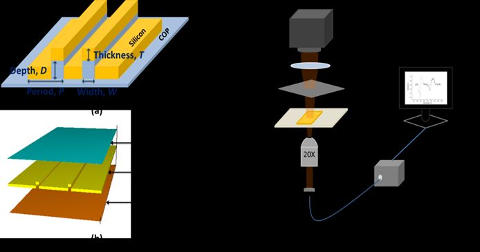
World Journal of Advanced Research and Reviews, 2023, 17(03), 272–275

References
[1]    Bravo, Javier, Lei Zhai, Zhizhong Wu, Robert E. Cohen, and Michael F. Rubner. "Transparent superhydrophobic
       films based on silica nanoparticles." Langmuir 23, no. 13 (2007): 7293-7298.
[2]    Cao, Lidong, Huirong Zhang, Zhaolu Zhou, Chunli Xu, Yongpan Shan, Yuqing Lin, and Qiliang Huang. "Fluorophore-
       free luminescent double-shelled hollow mesoporous silica nanoparticles as pesticide delivery vehicles."
       Nanoscale 10, no. 43 (2018): 20354-20365.
[3]    Xu, Ligang, and Junhui He. "Antifogging and antireflection coatings fabricated by integrating solid and
       mesoporous silica nanoparticles without any post-treatments." ACS applied materials & interfaces 4, no. 6
       (2012): 3293-3299.
[4]    Nair, Remya, Aby C. Poulose, Yutaka Nagaoka, Yasuhiko Yoshida, Toru Maekawa, and D. Sakthi Kumar. "Uptake
       of FITC labeled silica nanoparticles and quantum dots by rice seedlings: effects on seed germination and their
       potential as biolabels for plants." Journal of fluorescence 21 (2011): 2057-2068.
[5]    O’Farrell, Norah, Andrew Houlton, and Benjamin R. Horrocks. "Silicon nanoparticles: applications in cell biology
       and medicine." International journal of Nanomedicine 1, no. 4 (2006): 451-472.
[6]    Lee, Ji Eun, Nohyun Lee, Taeho Kim, Jaeyun Kim, and Taeghwan Hyeon. "Multifunctional mesoporous silica
       nanocomposite nanoparticles for theranostic applications." Accounts of chemical research 44, no. 10 (2011):
       893-902.
[7]    Farjadian, Fatemeh, Amir Roointan, Soliman Mohammadi-Samani, and Majid Hosseini. "Mesoporous silica
       nanoparticles: synthesis, pharmaceutical applications, biodistribution, and biosafety assessment." Chemical
       Engineering Journal 359 (2019): 684-705.
[8]    Hemmer, Eva, Pablo Acosta-Mora, Jorge Mendez-Ramos, and Stefan Fischer. "Optical nanoprobes for biomedical
       applications: shining a light on upconverting and near-infrared emitting nanoparticles for imaging, thermal
       sensing, and photodynamic therapy." Journal of Materials Chemistry B 5, no. 23 (2017): 4365-4392.
[9]    Bayir, Sumeyra, Alexandre Barras, Rabah Boukherroub, Sabine Szunerits, Laurence Raehm, Sébastien Richeter,
       and Jean-Olivier Durand. "Mesoporous silica nanoparticles in recent photodynamic therapy applications."
       Photochemical & Photobiological Sciences 17 (2018): 1651-1674.
[10]   Cheng, Wei, Junpeng Nie, Lv Xu, Chaoyu Liang, Yunmei Peng, Gan Liu, Teng Wang, Lin Mei, Laiqiang Huang, and
       Xiaowei Zeng. "pH-sensitive delivery vehicle based on folic acid-conjugated polydopamine-modified mesoporous
       silica nanoparticles for targeted cancer therapy." ACS applied materials & interfaces 9, no. 22 (2017): 18462-
       18473.

                                                                                                                   275
You can also read