Supplementary Materials for - Metasurface-driven OLED displays beyond 10,000 pixels per inch - Science
←
→
Page content transcription
If your browser does not render page correctly, please read the page content below
science.sciencemag.org/content/370/6515/459/suppl/DC1

 Supplementary Materials for
 Metasurface-driven OLED displays beyond 10,000 pixels per inch
 Won-Jae Joo*, Jisoo Kyoung†, Majid Esfandyarpour, Sung-Hoon Lee, Hyun Koo,
 Sunjin Song, Young-Nam Kwon, Seok Ho Song, Jun Cheol Bae, Ara Jo,
 Myong-Jong Kwon, Sung Hyun Han, Sung-Han Kim, Sungwoo Hwang,
 Mark L. Brongersma*
 *Corresponding author. Email: wj.joo@samsung.com (W.-J.J.); brongersma@stanford.edu (M.L.B.)

 Published 23 October 2020, Science 370, 459 (2020)
 DOI: 10.1126/science.abc8530

This PDF file includes:

 Materials and Methods
 Supplementary Text
 Figs. S1 to S14
 References
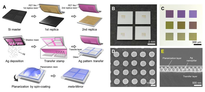
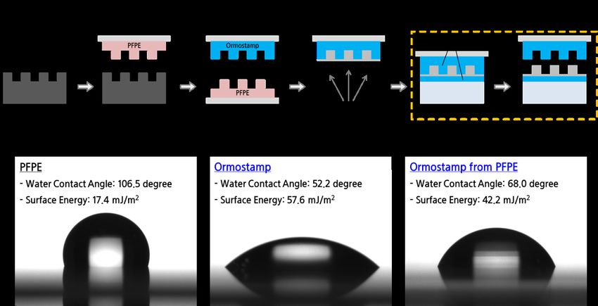
Materials and Methods

Meta-mirror fabrication using Nanoimprinting lithography

 The nanoimprint lithography (NIL) process is very useful for precise patterning of nano-
structures from tens to hundreds of nanometers in size, and it is applicable for Si wafers as well
as large glass substrates (square meters scale). To fabricate the nanopillars array of a meta-
mirror, the NIL process was applied (Figs. S3 and S4). First, a rectangular array (NIL master) of
nanoscale holes with a diameter of ~100 nm and a pitch of ~ 200 nm was fabricated on a Si
wafer by electron-beam lithography (EBL) and reactive ion etch (RIE) processes. The diameter
and pitch are the design parameters for manipulating the reflection phase and reflectance of
metasurface mirrors. Next, the primary polymer replica was made from the NIL master using a
fluorine-based UV curable resin (perfluoropolyether (PFPE) formulation, Solvay Co.), and the
secondary replica was prepared with a UV-curable acrylic resin (Ormostamp, Micro Resist
Tech.). The deposition of 200-nm-thick Ag layer on the secondary replica completes the meta-
mirror fabrication. Use of the primary fluorine-based resins makes it easy to delaminate the
polymer molds from the Si master without any surface treatment such as self-assembled
monolayer (Fig. S3). The secondary acrylic resin was carefully chosen due to its hydrophilic
properties, which facilitates the formation of Ag nanostructure on polymer molds by thermal
deposition. The Ag meta-mirror formed on the secondary replica mold was transferred into the
OLED glass substrate using a UV-curable adhesive resin. Finally, a polymer planarization layer
was spin-coated with UV-curable acrylic polymer (NIL210, Micro Resist Tech. GmbH) on the
meta-mirrors with nanopillars. Before building-up the OLED stack, the flattening of flattening
the nanostructures of meta-mirrors glass is necessary for ensuring the stable operation and long
lifetime of OLEDs.
 In the NIL process, the adhesion force between the mold and the substrate must be carefully
controlled to minimize defects. The surface energy of the acrylic mold used as the secondary
replica is noticeably lowered by the surface contact to the fluorinated first replica as can be seen
Fig. S4. The reduction of surface energy is due to the partial transfer of fluorinated molecules
into the 2nd replica and it facilitates the detachment of the Ag meta-mirror from the 2nd mold.
Figures S3D and S3E show scanning electron microscope (SEM) images of meta-mirrors
fabricated with the NIL method.

Meta-OLED fabrication

The organic light emitting device are built on the prepared meta-mirrors after spin-coating a
planarization layer. A 30-nm-thick indium tin oxide (ITO) layer is sputtered with electrode
patterns, and then multi-stacked organic layers are subsequently deposited. Finally, an AgMg
cathode (12 nm) and organic capping (70 nm) layer are thermally evaporated. The base pressure
of the evaporator chambers is 10-8 Torr. The multi-stacked structure of the OLED is as follows.
ITO (30 nm) / hole injection layer (HIL, 10 nm) / hole transport layer (HTL, 20 nm) / blue
emission material layer (EML, 6 nm) / buffer layer (4 nm) / red EML (3 nm) / green EML (12
nm) / buffer layer (4 nm) / blue EML(6 nm) / buffer layer (4 nm) / electron transport layer (ETL,
36 nm) / electron injection layer (EIL. 0.5 nm) / AgMg (10:1, 16 nm) / capping layer (CPL, 70
nm). The organic layers were carefully designed for satisfying both optical cavity condition and

 2
electric device condition. In the EMLs, fluorescent blue dopant and phosphorescent green and
red dopants were co-deposited with suitable host materials. Host materials usually play a role of
the charge transport and the exciton generation in EMLs. Buffer layers were inserted between the
blue EMLs and their interfacing layers in order to prevent unwanted exciton quenching. The
position, thickness and doping concentration of each RGB emitting layers were optimized to
produce a well-balanced white emission spectrum.
 As specific information on the OLED materials used here is beyond the subject of this study,
we simply present the photoluminescence spectra of RGB dopants in Fig. S8A. Generally, the
device performance of OLEDs strongly depends on the light emitting molecules and their
layered combination. Therefore, the reference white-OLED was prepared the same as the meta-
OLED, for fair comparison.

Numerical simulation of meta-mirrors

 The finite-difference time-domain (FDTD) simulation technique (FDTD Solutions,
Lumerical Solutions, Inc., Canada) was performed to understand the near-field coupling between
the incident light and meta-mirrors. The Ag bottom plate was thick enough (>300 nm) to block
any transmission. A rectangular array of cylindrical Ag nanopillars with a height h was placed on
the top of the plate. The top position of the Ag nanopillars was set to be z = 0 for all meta-
mirrors to easily compare the phase shift upon reflection and thereby the bottom position of the
post was set to be z = -h. We used the refractive index of Ag measured by ellipsometry. The
computational mesh size in the entire region was set as 1 nm in order to finely describe the
circular shape of the Ag nanopillar. A plane wave source was placed 1 µm above the top of
meta-mirror and a reflectivity monitor was located behind the source to remove the effect of
interference between the incident and reflected waves. The polarization direction of the incident
wave was TM. To display the near-field mode profile, a 2-dimensional field monitor (x-z plane
monitor) was also inserted. The boundary condition for the z-direction was a standard PML
(perfect matched layer) to eliminate unwanted reflection. Owing to the symmetric geometry of
our meta-mirror, the anti-symmetric (x-direction) and symmetric (y-direction) boundary
conditions were applied to reduce the simulation time to one fourth. Therefore, the actual
simulation was performed with only half of the period and the field map (figure 3B) in the
manuscript was drawn by translating and stitching the simulated region.

Numerical simulation of meta-OLED

 The FDTD simulation was also carried out for investigating the optical property of meta-
OLED structure. The reflective indice of organic semiconductor layers are commonly in the
range of 1.75 to 1.9. ETL (n=1.75), EMLs (n=1.75), HTL (n=1.9) and ITO (n=1.867+0.056i)
were subsequently placed on the meta-mirror. The optical absorption of these organic layers was
all ignored for simplicity. Capping layer (n=1.8) on AgMg cathode is fixed to 70-nm thickness.

 3
Measurements of the brightness and emission spectrum of OLEDs

The luminance and chromaticity of meta-OLED pixels were measured with a spectroradiometer
(SR-3AR, Topcon), which is widely used in the display field due to its high accuracy. The SR-
3AR has a collection numerical aperture of 0.0017, corresponding to a 0.1 degree measurement
angle. With this tool, light is collected from a circle-shaped detection area with a diameter of 0.5
mm. In order to perform quantitative measurement of the meta-OLED pixels, we fabricated
larger-sized meta-mirror pixels (0.6 × 0.6 mm2). For a qualitative analysis, small-size pixels of
0.3 mm or below were normally used to decrease the e-beam writing time. White OLED pixels
were also measured with the identical system and their RGB spectra were obtained through a
convolution with the spectral response function of color filters.

 4
Supplementary Text

Numerical simulation of the outcoupling efficiency

 We characterize the outcoupling behavior of meta-OLEDs with numerical simulation method
(Fig. S9). In terms of their light extraction, the metasurface mirror has positive and negative
aspects, simultaneously. Meta-mirror can be used to reduce the undesired plasmonic loss
occurring at the organic-metal interfaces. According to previous work [Ref.9. Nat. Nanotechnol.
9, 542-547 (2014), Ref.11. Nat. Commun. 9, 3224 (2018)], the nano-groove array of a meta-
mirror can be design to create a bandgap for surface plasmons across the visible wavelength
range and suppress the excitation of surface plasmon polariton waves. This provides an
opportunity to reduce undesired losses in the metal. On the other hand, the wide tuning of the
reflection phase on meta-mirror is accomplished by exciting gap plasmons in the grooves and
this comes at the cost of some optical losses. In microcavity devices with metamirrors, such
optical losses should be carefully managed. We find that there are typically trade-offs between
minimizing losses and achieving certain desirable emission properties, such as a narrow spectral
emission bandwidth.
 In order to calculate the outcoupling efficiency of meta-OLED and conventional top emission
(TE) and bottom emission (BE) OLEDs, we conduct finite-difference time-domain (FDTD)
simulations with a dipolar emitter. We set a 3-D simulation domain as 10 x 10 μm2 in lateral area
and 2 μm height with perfectly matched layers (PMLs) placed at the boundaries of the domain.
To quantify the outcoupling efficiency into the air, a far-field monitor with a size equal to the
domain-size is placed 20 nm above the cathode passivation layer (CPL), and the guided waves
including surface plasmon polaritons are measured by monitors placed on the sides of the
domain. As the far-field monitor is enough large to collect all the extracted photons around a full
180 degree, the angular-spectral emission behavior of devices is totally included in this result.
The very tiny box monitor, which fully covers the emissive dipole, measures the total power
radiated from the dipole. For two orthogonally oriented dipoles (TE∥ and TM∥), we simulate the
fraction of the total radiation flux of the emissive dipole that is coupled to the far-field (i.e. the
air), which reflects the out-coupling efficiency of the devices. To predict the behavior of an
isotropic emitter orientation, we assume fractions of 66.7% for the parallel and 33.3% for the
perpendicular dipole moments. Microcavity types of TE- and Meta-OLEDs are set to have a FP
resonance condition at 625 nm (surface normal), and BE-OLEDs have the same organic stacks as
the TE-OLEDs.
 The simulation result shows that all of the three different OLEDs have comparable
outcoupling efficiencies (25-28%) at the resonance wavelength of 625 nm. Taking into account
the fact that the meta-mirror has not been fully optimized yet for the highest reflectance, it is
clear that the outcoupling behavior of meta-OLEDs is not inferior to conventional OLED
devices. In fact, meta-OLEDs show a big difference from BE-OLED in their angular emission
pattern. The Lambertian emission behavior of BE-OLEDs results in a lower surface normal-
directional emission intensity, as compared to the more directional emission of microcavity type
devices. Compared to TE-OLED, the meta-OLED shows spectrally narrower outcoupling
characteristics. The spectral broadening of the microcavity OLEDs is closely linked to the large
angle dependence of the resonance wavelength in planar mirrors cavity (Fig. S13). We exactly
set the cavity length to have a resonance peak at 625 nm for surface normal light, but the
resonance peak is rapidly blue-shifted with increasing obliqueness of the angle. Considering the

 5
far-field monitor taking all the outcoupled light waves at 180 degree, a larger number of photons
can be counted at the shorter wavelength region than on resonance. On the other hand, the
resonance wavelength of the meta-cavity does not change significantly even at a large oblique
angles in Fig. S13. Accordingly, the meta-OLED exhibits a spectrally narrower emission
bandwidth and the peak position of spectral outcoupling efficiency does not move as much. As a
consequence, we can reasonably speculate that the positive and negative features of meta-
mirrors, the suppression of SPP loss and the gap plasmon resonance loss, equally contribute to
the outcoupling efficiency of the electric dipole radiation. In Fig. S9C, the waveguide mode is
mainly stimulated at a wavelength range away from on-resonance. The plasmonic absorption of
waveguide modes is more favorable than their extraction into air, in terms of color purity.

Numerical simulation for angular dependence of meta-OLED

We simulate the radiation pattern of μ-cavity OLEDs with respect to orthogonal dipole
orientations in Fig. S13. We set 3-D simulation domain as 10 × 10 μm2 in lateral area and 2 μm
height with perfectly matched layers (PMLs) placed at the boundaries of the domain. A far-field
monitor is placed 20 nm above the cathode passivation layer (CPL). The radiation of dipoles
with TM⊥ orientation is mostly coupled to surface plasmon or waveguide modes, and thus
contribute little to the far-field pattern. At two dipolar orientation components (TE∥ and TM∥),
spectral-angular radiation patterns are shown in Fig. S13. Flat mirror cavity (left panel) shows
typical angular dependency. This behavior is primarily caused by decreasing the effective cavity
length with increasing oblique angle. The meta-mirrors cavity (center and right panels) has
similar tendency but the amount of color shift is significantly reduced. The reduction in cavity
length is partially compensated with delayed reflection phase of meta-mirror. At 50-nm-high
cubic nanopillar, the color shift of TM oriented dipole is almost zero, which is ideal for displays.
One can find out the difference between conventional flat cavity and metasurface cavity at the
wavelength of near 450 nm. The 3rd blue resonance mode of flat-cavity disappears at the meta-
cavity, which is consistent with the high-order resonance suppression shown in Fig. S12. By
changing the nanopillar structure into nanocube, we further reduce the blue side-band in the red
pixel of meta-OLEDs. The FDTD calculation results also raise expectations for implementation
of full-color meta-OLED panel without using color filters.

 6
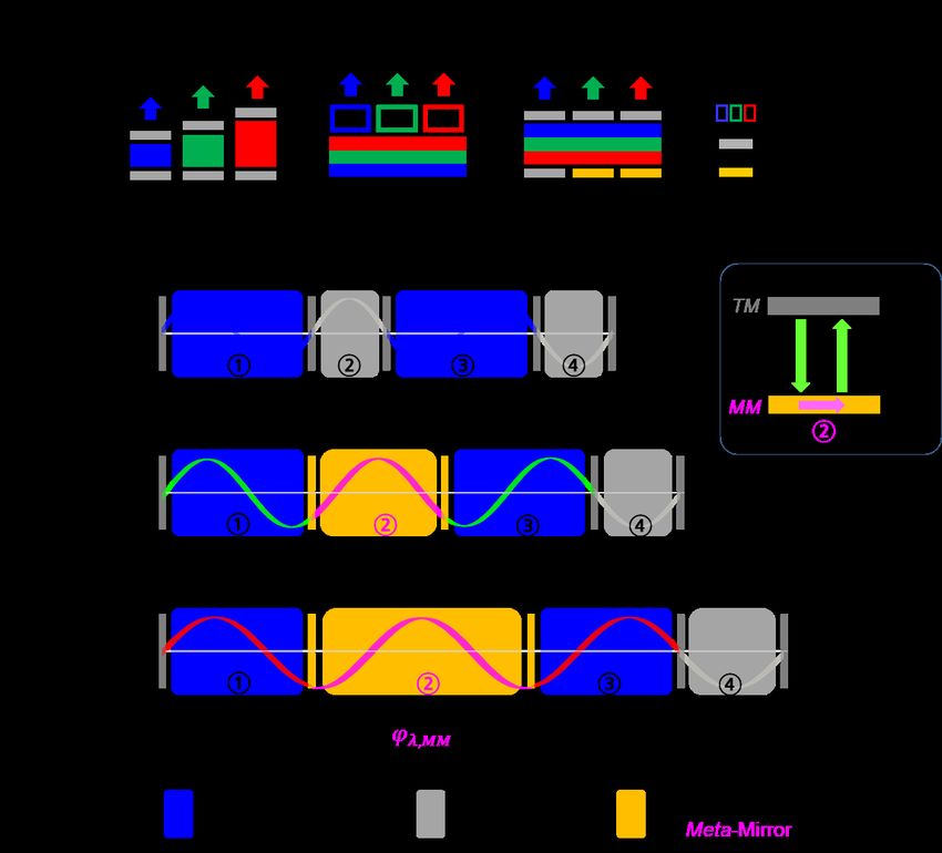
Fig. S1.
Metasurface driven, phase-controlled F-P cavity (Meta-cavity). (A) Device concepts of two
commercialized OLEDs in mobile displays (RGB-OLED) and TVs (color-filtered w-OLED), and
the new meta-OLED concept proposed here. In particular, the meta-OLED equips a phase
controllable metasurface mirror (Meta-Mirror, MM) in the green and red pixels. (B) Resonance
behaviors of RGB pixels in the meta-OLED. Conventional F-P cavity is adopted for blue (450 nm)
pixel, and meta-cavities embedding a meta-mirror on the bottom side is for green (520 nm) and
red (620 nm) pixels. In the inset, total one round-trip phases (①+②+③+④) should satisfy 6π
in these RGB OLED cavities with the same cavity length (Lc). The meta-cavity resonance is
dominantly controlled by the reflection phase ( , ) of the meta-mirror, not by cavity length
( , ). As the reflection phase of the meta-mirror is increased, the resonance wavelength increases
from blue to green and red colors. TM indicates the Ag top mirror and its reflection phase is
approximately π in the visible range.

 7
Fig. S2.
Reflection phase of meta-mirror required for resonating at an arbitrary wavelength in the visible
spectral range. For the red resonant cavity, a reflection phase of 2.2 π is needed, which means the
meta-mirror should delay the additional phase by 0.9π more than the reflection phase (1.3π ) of
the actual Ag flat mirror.

 8
Fig. S3.
Fabrication procedure for meta-mirrors by the nano-imprinting lithography (NIL) method. (A)
Process flow for meta-mirror fabrication. First, a silicon master is patterned by e-beam lithography
and two replications are made. Then, the meta-mirror fabrication is completed through the Ag
deposition on the 2nd replica. The fabricated meta-mirror is transferred onto the OLED test-cell
substrate (glass), and finally a planarization layer is formed on the nano-patterns. (B) Photo of 36
meta-mirrors transferred onto a glass substrate. Nine meta-mirrors in the 3×3 layout are placed in
each quadrant of the meta-OLED test-cell. (C) OM image of the 3×3 meta-mirrors with the size of
300 × 300 μm2. (D & E) Scanning electron microscope images (top and side views, respectively)
of the fabricated Ag meta-mirrors.

 9
Fig. S4.
Surface energy modification of NIL replica, Ormostamp (Micro Resist Tech.). (A) In the meta-
mirror’s transfer process, Ormostamp plays two important roles of the 2nd replica and transfer
resin, as highlighted in the yellow box. (B) Surface energy reduction (57.6 → 42.2 mJ/m2) of
Ormostamp by contact to the super-hydrophobic 1st replica, PFPE (Fluorolink, Solvay Co.). The
modified surface energy of 2nd replica facilitates the meta-mirror’s transfer to an OLED test-cell.

 10
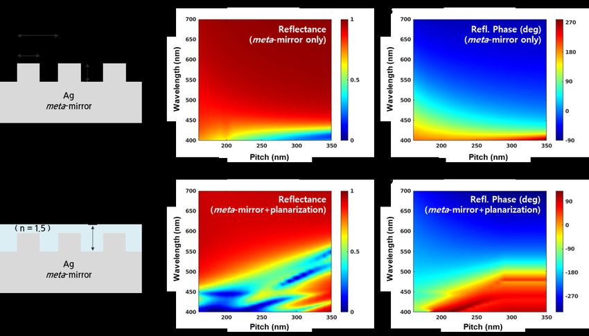
Fig. S5.
FDTD-simulated reflection properties of silver nanopillar rectangular arrays (metasurface mirrors)
with respect to the pitch between nanopillars. Cylindrical nanopillars have a diameter (D) of 100
nm and a height (H) of 80 nm. The pitch (P) between them varies from 160 to 350 nm. (A, B) The
Ag meta-mirror has an air gap between nanopillars. (C, D) The planarization layer (n = 1.5) is fully
covered on the top surface of the meta-mirror. (A, C) Calculated spectral reflectance map as a
function of the pitch between nanopillars. (B, D) Calculated reflection phase map as a function of
the pitch. As the pitch increases, the reflection phase overall decreases due to the weakening of the
gap resonance mode. By applying the planarization layer (n = 1.5) onto meta-mirror, the optical
resonance of incident light on meta-mirror becomes more complex in the blue spectral range.

 11
Fig. S6.
Calculated emission spectra of a color-filtered white-OLED (w-OLED/CF). (A) Spectral response
of already-known color filters. (B) Each RGB spectrum (colored line) is calculated through the
convolution of the spectral response (A) and the measured white-OLED emission spectrum
(dashed line).

 12
Fig. S7.
Hybrid RGB pixels of meta-OLEDs are divided into two parts, (1) an OLED part for generating
broadband light emission and (2) a meta-mirror part for tuning the resonance condition. In the
green and red pixels, the effective optical path lengths of meta-mirror part are significantly
increased through the excitation of gap plasmons in the nanostructured meta-mirror. The gray line
between the meta-mirror and OLED parts indicates a 30-nm-thick ITO layer which is included in
the optical thickness of OLED part. A polymeric planarization layer (n = 1.5) is placed onto the
flat mirror as well as the meta-mirrors. The EL image is cropped from (Fig. 1D).

 13
Fig. S8.
Purcell modified “internal emission power” calculated with a FDTD simulation. When three
different kinds of dopants for R, G and B colors are simultaneously placed at an antinode position
of the E-field for the cavity mode profile, only one dopant satisfies the resonance condition of the
cavity and its radiative emission rate is enhanced by the Purcell effect. The emission from the other
emitters is suppressed. (A) Normalized measured photoluminescence spectra (color lines) of RGB
dopants used here and their summation (grey line) conceptually representing a white electro-
luminescent spectrum. (B, C) Calculated Purcell factors, spontaneous emission powers of the
dipole emitter for specific OLED devices with a µ-cavity top emission structure (B) and ITO-based
bottom emission structure (C). The dipole orientation is 0.75 x + 0.25 z, where x- and z-
components are parallel and perpendicular to the mirror surface, respectively. (D-F) Purcell
modified internal emission power spectra which are simply calculated as the convolution of the
Purcell factor, FP(λ) in (B, C) and normalized internal emission, Io(λ) in (A). Unlike the ITO-based
OLED structure (grey lines) with a negligible Purcell effect, the µ-cavity structures significantly
alter the internal emission spectra (color lines), resulting in the improvement of the luminance
efficiency.

 14
Fig. S9.
FDTD calculated outcoupling efficiency of three different types of OLEDs, conventional
top-emission (TE) and bottom-emission (BE) OLEDs and our meta-OLED. (A)
Outcoupling efficiency of different kinds of OLEDs with respect to emission wavelength.
TE- and Meta-OLEDs are set to have F-P resonance condition at 625 nm on surface normal,
and BE-OLED has the same organic stacks with TE-OLED. All of them has comparable
outcoupling efficiency on resonance wavelength, because the far-field monitor integrates
all the extracted photons around a full 180 degree. (B) Their relative dipole radiation power
(Purcell) factor. Meta-OLED shows the two-fold higher Purcell factor than BE- OLED. (C)
Distribution of waveguide and plasmonic loss channels of the OLEDs with respect to two
orthogonal dipole orientations (TE∥ and TM∥). For the emitter having isotropic orientation,
a fraction of 66.7% parallel and 33.3% perpendicular dipoles is expected to totally
contribute to the output intensity. The blue-shifted maxima of TE-OLED is due to the blue-
shift behavior of resonance peak at oblique angle.

 15
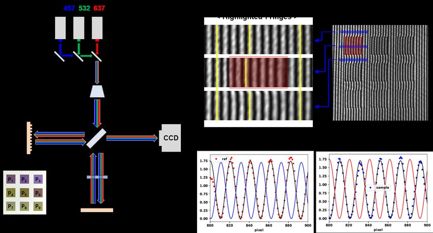
Fig. S10.
Reflection phase measurement of meta-mirrors. (A) Schematic diagram of the standard Michelson
interferometer, in which laser sources have emission wavelengths close to the RGB colors of
displays. (B) The measured interference patterns of the 3×3 meta-mirrors. The interference
patterns across the three blue bars are magnified on the left side of the image. The top and bottom
reference patterns are taken from a flat (i.e. smooth) Ag surface and the middle signal pattern is
across the nano-grooved meta-mirror (red box). (C) The sinusoidal curve fitting from the
amplitude profiles of reference and signal patterns. The phase difference between the reference
and signal curves results from the phase delay occurred on the nanopillars array.

 16
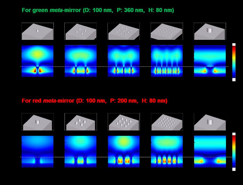
Fig. S11.
FDTD-calculated H-field distribution of the submicron scale meta-mirrors for the green and red
pixels, in which the incident wavelengths are 520 and 620 nm, respectively. The strong field
confinement appears from the single nanopillar in the green cavity and from the 3×3 nanopillars
in the red cavity. As compared to the periodic structure, the submicron scale array confines the
field more strongly in the gap region, but the difference can be simply recovered through a slight
tuning of the nanopillar design. Thus, the green and red pixels of meta-OLEDs require a minimum
of 2×2 and 3×3 nanopillar arrays, respectively, which are 0.7×0.7 μm2 in size.

 17
Fig. S12.
Higher-order resonance suppression in OLED μ-cavity by the wavelength-dependent phase
response of the meta-mirrors. (A) The resonance modes of a conventional FP cavity with flat
mirrors and a meta-cavity with metasurface mirrors which satisfy the 2nd-order resonance
condition at 620 nm. Because the 3rd-order blue resonant condition is very close to the 2nd red
condition, the blue emission in the red cavity can seriously impair the color purity, when the white
emitting layers are placed within the cavity. In the meta-cavity, the 3rd-order resonance wavelength
is notably blue-shifted as compared to that of the flat cavity and the free-spectral range between
cavity resonances is increased. This results from a wavelength-dependent reflection phase of meta-
mirrors that be engineered for many cavity applications. (B) Measured emission spectra from two
different types of red μ-cavity OLEDs. The higher-order resonance suppression of the metasurface
provides a unique way for not using additional color filters. (C) The RGB spectra of meta-OLEDs
with a newly designed, nano-cubic meta-mirror, in which the blue side-bands are further reduced.
This nano-cube pattern is one of possible, judiciously-optimized meta-mirror designs.

 18
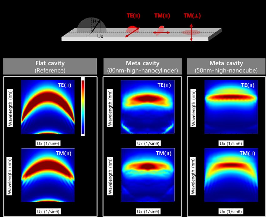
Fig. S13.
FDTD-calculated angle-dependent emission behavior of meta-OLEDs and conventional
microcavity OLEDs. (A) Definition of viewing angle and dipole orientations. The Ux is a direction
unit vector. The direction unit vector (Ux) is defined as sin θ. (B) The calculated angular-spectral
radiation patterns of flat-mirror cavity (left panel) and meta-mirror cavities (center and right
panels). The TM⊥ oriented dipole is not shown due to its negligibly weak power in far-field mode.
In the flat mirror cavity (left panel), resonance wavelength is blue-shifted as the viewing angle
increases, which is the typical behavior for a microcavity. On the other hand, the meta-mirror
cavity (center and right panels) have a similar tendency but the amount of color shift is significantly
reduced.

 19
Fig. S14.
Measured angular-spectral emission behavior of meta-OLEDs and conventional micro-cavity
OLEDs. Viewing angle ( ) is defined as the tilt angle of the sample from the axis normal.
Spectroradiometer has a working distance of 30 cm and a measurement angle of 0.1o. The peak
wavelength of meta-OLED shifts from 618.5 to 613.2 nm (∆λ = 5.3 nm) at 45o tilt angle. On the
other hand, in the flat-OLED, the peak position moves from 626.8 to 616.1 nm (∆λ = 10.7 nm).

 20
References and Notes
1. A. Perot, C. Fabry, On the Application of Interference Phenomena to the Solution of Various
 Problems of Spectroscopy and Metrology. Astrophys. J. 9, 87–115 (1899).
 doi:10.1086/140557
2. J. Barnes, A simple Fabry and Perot interferometer. Science 30, 29–30 (1909).
 doi:10.1126/science.30.757.29 Medline
3. E. F. Schubert, N. E. J. Hunt, M. Micovic, R. J. Malik, D. L. Sivco, A. Y. Cho, G. J. Zydzik,
 Highly efficient light-emitting diodes with microcavities. Science 265, 943–945 (1994).
 doi:10.1126/science.265.5174.943 Medline
4. N. Jukam, A wavelength-size tunable Fabry–Pérot laser. Nat. Photonics 13, 823–825 (2019).
 doi:10.1038/s41566-019-0555-7
5. R. Meerheim, R. Nitsche, K. Leo, High-efficiency monochrome organic light emitting diodes
 employing enhanced microcavities. Appl. Phys. Lett. 93, 043310 (2008).
 doi:10.1063/1.2966784
6. R. Ameling, D. Dregely, H. Giessen, Strong coupling of localized and surface plasmons to
 microcavity modes. Opt. Lett. 36, 2218–2220 (2011). doi:10.1364/OL.36.002218
 Medline
7. A. M. Shaltout, J. Kim, A. Boltasseva, V. M. Shalaev, A. V. Kildishev, Ultrathin and
 multicolour optical cavities with embedded metasurfaces. Nat. Commun. 9, 2673 (2018).
 doi:10.1038/s41467-018-05034-6 Medline
8. J. Flannery, R. Al Maruf, T. Yoon, M. Bajcsy, Fabry-Pérot cavity formed with dielectric
 metasurfaces in a hollow-core fiber. ACS Photonics 5, 337–341 (2018).
 doi:10.1021/acsphotonics.7b01154
9. M. Esfandyarpour, E. C. Garnett, Y. Cui, M. D. McGehee, M. L. Brongersma, Metamaterial
 mirrors in optoelectronic devices. Nat. Nanotechnol. 9, 542–547 (2014).
 doi:10.1038/nnano.2014.117 Medline
10. V. A. Fedotov, A. V. Rogacheva, N. I. Zheludev, P. L. Mladyonov, S. L. Prosvirnin, Mirror
 that does not change the phase of reflected waves. Appl. Phys. Lett. 88, 091119 (2006).
 doi:10.1063/1.2179615
11. M. Esfandyarpour, A. G. Curto, P. G. Kik, N. Engheta, M. L. Brongersma, Optical emission
 near a high-impedance mirror. Nat. Commun. 9, 3224 (2018). doi:10.1038/s41467-018-
 05505-w Medline
12. N. Yu, F. Capasso, Flat optics with designer metasurfaces. Nat. Mater. 13, 139–150 (2014).
 doi:10.1038/nmat3839 Medline
13. Y.-W. Huang, H. W. H. Lee, R. Sokhoyan, R. A. Pala, K. Thyagarajan, S. Han, D. P. Tsai, H.
 A. Atwater, Gate-Tunable Conducting Oxide Metasurfaces. Nano Lett. 16, 5319–5325
 (2016). doi:10.1021/acs.nanolett.6b00555 Medline
14. C. Xiang, W. Koo, F. So, H. Sasabe, J. Kido, A systematic study on efficiency enhancements
 in phosphorescent green red and blue microcavity organic light emitting devices. Light
 Sci. Appl. 2, e74 (2013). doi:10.1038/lsa.2013.30
15. M. Wang, J. Lin, Y.-C. Hsiao, X. Liu, B. Hu, Investigating underlying mechanism in spectral
 narrowing phenomenon induced by microcavity in organic light emitting diodes. Nat.
 Commun. 10, 1614 (2019). doi:10.1038/s41467-019-09585-0 Medline
16. C.-W. Han, J.-S. Park, Y.-H. Shin, M.-J. Lim, B.-C. Kim, Y.-H. Tak, B.-C. Ahn, Advanced
 Technologies for large-sized OLED TV. SID Symp. Dig. Tech. Pap. 45, 770–773 (2014).
 doi:10.1002/j.2168-0159.2014.tb00202.x
17. H.-J. Kim, M.-H. Shin, H.-G. Hong, B.-S. Song, S.-K. Kim, W.-H. Koo, J.-G. Yoon, S.-Y.
 Yoon, Y.-J. Kim, Enhancement of optical efficiency in white OLED using the patterned
 photoresist film dispersed with quantum dot nanocrystals. J. Disp. Technol. 12, 526–531
 (2016). doi:10.1109/JDT.2015.2503401
18. A. Ghosh, E. P. Donoghue, I. Khayrullin, T. Ali, I. Wacyk, K. Tice, F. Vazan, L. Sziklas, D.
 Fellowes, R. Draper, Directly Patterned 2645 PPI full color OLED microdisplay for head
 mounted wearables. SID Symp. Dig. Tech. Pap. 47, 837–840 (2016).
 doi:10.1002/sdtp.10805
19. W. Song, J. You, C.-Y. Wu, L. Wang, Y. Shen, B. Bo, W. Quan, C. Luo, D. Yu, W. Li, H.-T.
 Shih, Z. Wu, 3-Stacked Top-Emitting White OLEDs with super-wide color gamut and
 high efficiency. SID Symp. Dig. Tech. Pap. 50, 46–49 (2019). doi:10.1002/sdtp.12852
20. B. E. A. Saleh, M. C. Teich, “Resonance optics” in Fundamentals of Photonics (Wiley, ed. 2,
 2019), pp. 436–446.
21. H. Cho, J. Chung, J. Song, J. Lee, H. Lee, J. Lee, J. Moon, S. Yoo, N. S. Cho, Importance of
 Purcell factor for optimizing structure of organic light-emitting diodes. Opt. Express 27,
 11057–11068 (2019). doi:10.1364/OE.27.011057 Medline
22. S. Hofmann, M. Thomschke, B. Lüssem, K. Leo, Top-emitting organic light-emitting diodes.
 Opt. Express 19 (Suppl 6), A1250–A1264 (2011). doi:10.1364/OE.19.0A1250 Medline
23. E. Jang, Y. Kim, Y.-H. Won, H. Jang, S.-M. Choi, Environmentally Friendly InP-Based
 Quantum Dots for Efficient Wide Color Gamut Displays. ACS Energy Lett. 5, 1316–1327
 (2020). doi:10.1021/acsenergylett.9b02851
24. D. Sievenpiper, L. Zhang, R. F. J. Broas, N. G. Alexopolous, E. Yablonovitch, High-
 impedance electromagnetic surfaces with a forbidden frequency band. IEEE Trans.
 Microw. Theory Tech. 47, 2059–2074 (1999). doi:10.1109/22.798001
25. S. I. Maslovski, M. G. Silveirinha, Nonlocal permittivity from a quasistatic model for a class
 of wire media. Phys. Rev. B 80, 245101 (2009). doi:10.1103/PhysRevB.80.245101
26. K. Kumar, H. Duan, R. S. Hegde, S. C. W. Koh, J. N. Wei, J. K. W. Yang, Printing colour at
 the optical diffraction limit. Nat. Nanotechnol. 7, 557–561 (2012).
 doi:10.1038/nnano.2012.128 Medline
27. J.-H. Lee, K.-R. Kim, C.-S. Kim, “Subpixel rendering without color distortions for diamond-
 shaped PenTile displays” in Proceedings of the 2017 IEEE International Symposium on
 Circuits and Systems (ISCAS) (IEEE, 2017), doi:10.1109/ISCAS.2017.8050386.
28. K.-T. Lee, S. Y. Han, Z. Li, H. W. Baac, H. J. Park, Flexible High-Color-Purity Structural
 Color Filters Based on a Higher-Order Optical Resonance Suppression. Sci. Rep. 9,
 14917 (2019). doi:10.1038/s41598-019-51165-1 Medline
29. G. Tan, J.-H. Lee, S.-C. Lin, R. Zhu, S.-H. Choi, S.-T. Wu, Analysis and optimization on the
 angular color shift of RGB OLED displays. Opt. Express 25, 33629–33642 (2017).
 doi:10.1364/OE.25.033629
You can also read