SYNTHESIS AND CHARACTERIZATION OF NANOCOATINGS THIN FILMS OF TIO2, SIO2, ZNO, AND CUO BY SPUTTERING DEPOSITION
←
→
Page content transcription
If your browser does not render page correctly, please read the page content below
Journal of Mechanical Engineering Research and Developments
ISSN: 1024-1752
CODEN: JERDFO
Vol. 44, No. 7, pp. 40-46
Published Year 2021

 Synthesis and characterization of nanocoatings thin films
 of TiO2, SiO2, ZnO, and CuO by sputtering deposition
 Haitham M. Wadullah†∗, Omer Khalil Ahmed†, Sohaib Hassan Mohammed†
 †
 Engineering Technical College of Mosul/ Northern Technical University, Iraq
 ‡
 Technical Institute / Hawija, Northern Technical University, Iraq

 *Corresponding Author email: dr.haitham@ntu.edu.iq, hai_moh2004@yahoo.com

ABSTRACT

This work is aiming to synthesis and characterize of nanocoating thin films prepared by sputtering deposition at
optimal conditions on various substrates. Magnetron sputtering deposition technique has been used to deposit
nanocoating thin films of TiO2, SiO2, ZnO, and CuO on different substrates (stainless steel 316L, commercially
pure Ti, Si-Wafer (100), and glass substrates). Surface morphology, crystal structure and size, and films
elements deposited have been investigated using SEM, XRF, and XRD characterization technique respectively.
From the findings of SEM photographs, the microstructure is uniform and the surface is free of defects or
micro-cracks. The deposited thin films have a nanostructure and nanoparticle grain size of 60-90 nm,
according to X-ray diffraction patterns. Also, all thin films have a crystal structure aligned in different
directions matched to the standard phases peaks. The elements of each film deposit are specific objectives
by the XRF peaks that are produced.

KEYWORDS

Nanocoatings, 100nm Thin Films, Sputtering Deposition, TiO2, CuO, ZnO, SiO2

INTRODUCTION

As a result of unique atom material features relative to bulk materials, nanotechnology applications have
increased tremendously. The nanocoatings description is used whether the coated thickness is in nanometre
scales or the structure is in nanostructure scales from (1-100nm), which is the ultimate obstacle in materials
science nowadays. Nanocoatings have superior properties and characteristics due to the quantum size effect
[1]. Nanocoating thin films are formed employing nanocoating facilities such as atomic layer deposition,
sputtering deposition, and pulsed laser deposition to build coating layers with varied nano thickness to improve
attributes not observed in traditional coating procedures [2, 3]. Masayoshi [4] depended that it is a few thousands
of atoms, and the structure and properties gotten are not present in traditional coatings methods. In addition to
high corrosion resistance and biocompatibility, nanocoatings of ceramic materials may be synthesized to
make the surface bioactive and chemically inert. For that, nanostructured processing is now used in a variety
of research and technology materials due to its unique electrical, optical, biological and mechanical properties.
Arkadiusz [5] point out that some of the Nanostructure have scattering losses, so they can be used in the
plasmonic, biosensor, and functional material applications. The most popular applications of nanomaterials,
according [6], are microelectromechanical and nanoelectromechanical structures, bioengineering,
biomedical applications, nonlinear optical properties generators, and surface-enhanced Raman scattering
instruments.

Kumar [7] reviewed that CuO has an advantageous and exciting material for system biomedical applications due
to its nontoxicity and ample abundance of its constituents. It has also been studied extensively for electrical uses,
including solar energy conversion, optoelectronics, batteries, sensors, semiconductors, and catalysis. Sawsen et
al. [8] study the Properties of TiO2 thin films deposited by Rf reactive magnetron sputtering on biased
substrates. It reviewed that titanium dioxide (TiO2) has a powerful transition metal oxide that's useful
for catalysis, computing, photonics, sensing, medicine, and controlled drug release, among other things. It has
excellent optical

 40
Synthesis and characterization of nanocoatings thin films of TiO2, SiO2, ZnO, and CuO by sputtering deposition

and electrical properties, and ease of mass processing. That was TiO2 is one of the most commonly used
photocatalysts in many areas, including antibacterial applications, water purification, decomposition of different
organic compounds, and solar cell applications. Ivan et al. [9] and Joaquim et al. [10] displays that Silicon dioxide
(SiO2) is a commonly used element in many scientific fields and a variety of applications, such as medicinally
because it has excellent chemical and biological compatibility furthermore to an antimicrobial effect, for that its
implanted in the brain, food industry and preservation and, microelectronics, and communication. They have been
examined in both crystalline and amorphous forms. Wadullah et al. [2] defined the deposition of 25nm and 50nm
thin films of Alumina, Titania, and Alumina/Titania multilayer thin films on Co-Cr alloys using the Atomic Layer
Deposition (ALD) technique (ASTM F75).

Good thin-film durability, homogeneity, and thin-film properties have been found, as well as no defects or micro
cracks. Al2O3 ALD films had lower surface roughness values and greater thin film thickness control than TiO2
and Al2O3/ TiO2. Coating the surface of implant alloys improves corrosion resistance while also improving
biocompatibility according to Priyadarshini et al. [11]. Wadullah et al. [12] explored platinum (Pt) thin films with
thicknesses of 17nm and 34nm deposited by sputtering on Ni-Cr alloy substrates. The findings indicate that a
nanostructured and defect-free Pt thin film can be deposited on artificial saliva at 37°C, as well as increased
localized electrochemical corrosion resistance. According to Masayoshi et al. [4], metallic nanoparticle synthesis
has gotten a lot of attention in recent years due to their ability as green and cost-effective synthesis tools, as well
as the biological molecules aimed at them. Vyas S. [13] discuss the wide range of Zinc oxide application which
are including robotics, healthcare, food processing, biomedicine, and biosensors as one of the most important
parts. ZnO has biocompatible and non-toxic behavior which is the main points for the biological role of the
element to be preserved. Electrically, transparent conducting oxides, gas sensors, light-emitting diodes, lasers,
and photodetectors are only a few of the ZnO applications.

Several authors [14] have researched in thin film depositions, however, there are only a few experiments that have
dealt with the deposition of various thin films by sputtering on various substrates. For that, this work is aiming to
prepare nanocoating thin films of TiO2, SiO2, ZnO, and CuO with 100 nm thickness by sputtering deposition on
various substrates (stainless steel 316L, commercially pure Ti, Si-100, and glass substrates) at optimal conditions.
In addition to analyzing the thickness, roughness, surface morphology, phases, and deposited nanocoatings
elements. Where, the paper is a supplement to a Nanoceoatings thin film deposition program, which began with
Al2O3, TiO2, and Al2O3 / TiO2, Au., and Pt. films for different applications. The new paper is constructed in the
following manner. The experimental setup, as well as the procedure, are described in Section 2. The findings are
examined and defined in Section 3. Finally, in Section 4, the new research's findings are addressed.

EXPERIMENTATION WORK

Materials and Preparations

In this experiment, the materials used are stainless steel 316L, commercially pure titanium (Ti–6Al– 4V), Si-
Wafer(100), and glass specimens with dimensions of 2.5 x 1.9 x 0.1 cm2 . ASTM D4708 - 12 has been used to
prepare the specimens. Plates were cut into samples using a wire cut machine with a slow flow rate and cutting
speed, as well as cutting fluid has been used to prevent the cutting from heating up. SiC papers with grits of 400,
600, 800, and 1000 were used to grind samples face. They were then washed with purified water. For Stainless
steel 316L and Al alloys, they have been ultrasonically cleaned for 60 minutes with acetone, washed with methanol
/ de-ionized water to eliminate any organic pollutants, and eventually dried with hot air before being placed in the
deposition chamber. For Si-Wafer(100) and glass specimens, before being put have been chemically washed with
a diluted 5% HF solution and dried with N2 gas. The composition of materials has been determined by chemical
analysis in the Ministry of Science and Technology, Iraq.

Deposition Facility and Conditions

Different Targets have been used with high purity in a magnetron sputtering deposition unit according to the type
of film needed. After the device was calibrated with different goals and power at Iraq's Ministry of Science and
Technology, the calibration graph has been used to guess the power/time needed to deposit a certain thickness of

 41
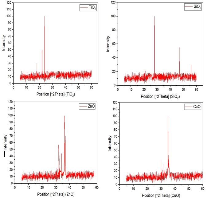
Synthesis and characterization of nanocoatings thin films of TiO2, SiO2, ZnO, and CuO by sputtering deposition

film which is 100 nm on different substrates selected. The optimal deposition conditions were 2.8x10⁻⁷ Torr
vacuum base pressure, 2nm/min rate, 20 standard cubic centimeter per minute (sscm) Argon steam, and 4 Torr
pressure during the deposition. The thin film deposited annealed for 1h in an argon setting for all films used and
according to the scheduled temperature related to the type of films.

Characterization Facilities and Methods

For studying the thin films surface uniformity, SEM (scanning electron microscope) has been used with an
imaging system monitored by sophisticated tools. The TFProobe spectroscopic unit has been used in conjunction
with algorithms to determine the thickness of films. The Cu-K radiation has been used in an X-ray Diffraction
(XRD) from Philips which is used to estimate the average crystallite size. The Debye–Scherrer method has been
used to calculate the average crystallite, as follows:

(D = ) (1)

Where :D is the average crystallite size, γ is the X-ray wavelength of the incident radiation (CuK= 0.15406 nm),
k is the shape factor with a typical value of 0.89, β is the line broadening full width at half maximum (FWHM) in
radians, and θ is the Bragg angle. The high-intensity peak (101) has been chosen for the calculation of crystallite
size. The non-destructive analytical method XRF (X-ray fluorescence) is used to determine the elemental
composition of thin films. By analyzing the fluorescent X-ray released from a sample as it is excited by a primary
X-ray light, XRF analyzers can determine the chemistry of a sample. Each element in a sample emits a series of
fluorescent X-rays that are unique to it.

RESULTS AND DISCUSSION

The main challenge of this research is to make uniform and homogeneous thin films nanostructures using
magnetron sputtering deposition. To compare the morphology of thin films, different substrates (stainless steel
316L, commercially pure titanium, Si-Wafer (100), and glass) have been used. SEM, XRD, and XRF have been
used to analyze the surface morphology, crystal structure, and elements of the deposited films respectively. Figure
1 shows a micrograph of SEM of 100 nm thin film after annealing for 1h in an argon setting, It appears that the
films haven't micro-cracks or defect and its homogeneous at 400 nm magnification. Fig. 1a & b shows TiO2 and
SiO2 thin film, which has a very fine and uniform aggregation as conformed by researchers [15, 16]. Fig. 1 b & c
appears ZnO and CuO thin film, which has a different morphology compared with the other films; more coarse
grains with larger aggregation, which is matched the findings of the researcher [17].

 Figure 1. SEM results of thin films deposited; a) TiO2 thin film, b) SiO2 thin film, c) ZnO thin film, d) CuO
 thin film

XRD has been used to determine the phase structure of the deposited films. The diffraction patterns of deposited
films as seen in Figure 2. In all diffraction patterns of TiO2, SiO2, ZnO, and CuO films, Fig. 2, there is TiO2

 42
Synthesis and characterization of nanocoatings thin films of TiO2, SiO2, ZnO, and CuO by sputtering deposition

peaks at 2θ equal to (18 o, 22 o, 23 o) and sharp anatase peak (101) is at 2θ =25o. The results are confirmed by
the researcher [18]. The sharp peak of SiO2 shows at 2θ = 37 o, is formed of (002), and the other peaks at 2θ equal
to (47 o, 56 o). ZnO peak at 2θ equal to (32 o,34 o, 37 o) and CuO peak at 2θ equal to ( 30 o, 32 o, 35 o) and
sharp anatase peak (111) for CuO film is at 2θ =35 as confirmed by the researcher [17]. The type of the XRD
used in this investigation is more sensitive to the thin films although the thickness was 100 nm. The surface grain
size was in the range of 60-90 nm and the size of the crystal are approximately 8, 14, 20, and 35 nm for TiO2,
SiO2, ZnO, and CuO respectively

 Figure 2. XRD results of thin films deposited; a) TiO2 thin film, b) SiO2 thin film, c) ZnO thin film, d) CuO
 thin film

XRF (X-ray fluorescence) has been used to determine the elemental composition of thin films deposited as seen
in Fig 3 a, b, c &d. For the TiO2 film, the XRF results appear the max. peak of Ti element compared with other
elements. Which is related to the TiO2 film deposited on the substrates as verified by the researcher [15]. The
XRF of the SiO2 film shows max. peak of Si. The max. the peak of ZnO film is Zn, and Cu is the max. peak for
CuO film. All of these results are confirmed with the type of film deposited.

 43
Synthesis and characterization of nanocoatings thin films of TiO2, SiO2, ZnO, and CuO by sputtering deposition

 b)

 c)

 d)

Figure 3. XRF results of thin films deposited; a) TiO2 thin film, b) SiO2 thin film, c) ZnO thin film, d) CuO thin
 film

CONCLUSION

In the current study, nanocoating thin films of TiO2, SiO2, ZnO, and CuO have been deposited on various
substrates (stainless steel 316L, commercially pure Ti, Si-Wafer(100), and glass substrates) using a magnetron
sputtering deposition process at optimal conditions. The deposition environments have been tailored for various
targets during deposition at 2.8x10⁻⁷ Torr vacuum base pressure, 2nm/min rate, 20 standard cubic centimeter per
minute (sscm) Argon steam, and 4 Torr pressure. The SEM, XRD, and XRF have been used for nanocoated
substrates. The following findings can be drawn from this research:
 1. The thin films deposited haven't micro-cracks or defect with a uniform and homogeneous structure at
 400 nm magnification.
 2. SEM results indicated that the films have a very fine aggregation for TiO2 and SiO2 films compared
 with more coarse grain and larger aggregation for ZnO and CuO films.
 3. Nanostructure and nanoparticle grain size of 60-90 nm with a crystal structure arranged in different
 directions matched to the standard phases characterized in this study.
 4. A unique element of each film deposit identified by XRF peaks as an indication of the films deposited.

CONFLICTS OF INTEREST

The authors identify and declare that there is no conflict of interest.

 44
Synthesis and characterization of nanocoatings thin films of TiO2, SiO2, ZnO, and CuO by sputtering deposition

ACKNOWLEDGEMENT

We'd like to thank the Northern Technical University, Iraq and the Ministry of Science and Technology, Iraq for
their help in demonstrating this work.

REFERENCES

[1] H.M. Wadullah, S.M. Sultan, and O.M. Ali, “Electrochemical Corrosion Resistance and In Vivo Bioactivity
 of Nickel, Silver and Cobalt Nanoparticles Materials for Medical Applications”, Journal of Mechanical
 Engineering Research and Development, Vol. 44, No. 4, Pp. 362-367, 2021.

[2] H.M. Wadullah, S.A. Ajeel, and M.K. Abbass, “Synthesis and Characterization of Nanocoatings Thin films
 by Atomic Layer Deposition for Medical Applications”, 2nd International Conference on Sustainable
 Engineering Techniques (ICSET 2019) IOP Publishing: Materials Science and Engineering, 518, Pp. 032057,
 2019. https://doi:10.1088/1757-899X/518/3/032057.

[3] H.M. Wadullah, S.A. Abualnoun, M.K. Abbass, and M.Y. Hussein, “Corrosion of platinum nanocoatings thin
 films deposited by Sputtering Deposition Method for medical applications”, International Journal of
 Engineering & Technology, Vol.7, No. 4.37, Pp. 63-66, 2018.

[4] M. Tanaka, S. Saito, R. Kita, J. Jang, Y. Choi, J. Choi and M. Okochi, “Array-Based Screening of Silver
 Nanoparticle Mineralization Peptides”, International Journal of Molecular Sciences, Vol. 21, Pp. 2377, 2020.
 https://doi.org/10.3390/ijms21072377.

[5] A. Ciesielski, M. Trzcinski and T. Szoplik, “Inhibiting the Segregation of Germanium in Silver Nanolayers”,
 Crystal’s journal, Vol. 10, No. 262, Pp. 1-11, 2020. https://doi.org/10.3390/cryst10040262

[6] L. Zhou, H. Fu, T. Lv, C. Wang, H. Gao, D. Li, L. Deng and W. Xiong, “Nonlinear Optical Characterization
 of 2D Materials. Nanomaterials Journal, Vol. 10, No. 2263, Pp. 1-38, 2020.

[7] S.K. Kumar, S. Murugesan, S. Suresh, and S.P. Raj, “Nanostructured CuO Thin Films Prepared through
 Sputtering for Solar Selective Absorbers”, Journal of Solar Energy Volume, Article ID 147270, 2013.
 http://doi.org/10.1155/2013/147270.

[8] S. Nezara, S. Nadia, S. Samira, F. Mohammed, M. Mogtaba, A. Nadia, B. Laoufi, and T. Nouar, “Properties
 of TiO2thin films deposited by Rf reactive magnetron sputtering on biased substrates”, Applied Surface
 Science J., Vol. 395, Pp. 172-179, 2017.

[9] I. Radović, Y. Serruys, Y. Limoge and N. Bibić, “Reactive sputtering deposition of SiO2 thin films”, J. Serb.
 Chem. Soc., Vol. 73, No. 1, Pp. 121–126, 2008.

[10] J.O. Carneiro, F. Machado, L. Rebouta, M.I. Vasilevskiy, S.L. Méndez, V. Teixeira, M.F. Costa and A.P.
 Samantilleke, “Compositional, Optical and Electrical Characteristics of SiOx”, Thin Films Deposited by
 Reactive Pulsed DC Magnetron Sputtering Coatings, Vol. 9, Pp. 468, 2019.
 https://doi:10.3390/coatings9080468.

[11] B. Priyadarshini, M. Rama, Chetan and U. Vijayalakshmi, “Bioactive coating as a surface modification
 technique for biocompatible metallic implants: a review”, Journal of Asian Ceramic Societies, Vol. 7, No. 4,
 Pp. 397-406, 2019. https://doi.org/10.1080/21870764.2019.1669861.

[12] H.M. Wadullah, M.K. Abbass, S.A. Ajeel, and M.Y. Hussein, “Evaluation the corrosion resistance of Pt.
 thin films for medical applications”, AIP Conference Proceedings, Vol. 2213, Pp. 020319, 2020.
 https://doi.org/10.1063/5.0000444.

[13] S. Vyas, “A Short Review on Properties and Applications of Zinc Oxide Based Thin Films and Devices ZnO
 as a promising material for applications in electronics, optoelectronics, biomedical and sensors”, Johnson
 Matthey Technol. Rev., Vol. 64, No. 2, Pp. 202. 2020. https://doi:10.1595/205651320x15694993568524

[14] S.H. Mohammed, O.K. Ahmed, and H.M. Wadullah, “A Review Improve the Solar Collectors Efficiency by
 Thin Films Techniques”, Journal of Mechanical Engineering Research and Developments, Vol. 44, No. 4, Pp.
 178-193, 2021.

 45
Synthesis and characterization of nanocoatings thin films of TiO2, SiO2, ZnO, and CuO by sputtering deposition

[15] O.G. Simionescu, R. Cosmin, O. Tutunaru, V. Ion, O. Buiu, and A. Andrei, “RF Magnetron Sputtering
 Deposition of TiO2 Thin Films in a Small Continuous Oxygen Flow Rate”, Coatings, Vol. 9, Pp. 442, 2019.
 https://doi:10.3390/coatings9070442.

[16] J.O. Carneiro, F.S.M.L. Rebout, S. Lanceros-Méndez, V. Teixeira, M.F. Costa and P. Anura, “Samantilleke,
 Compositional, Optical and Electrical Characteristics of SiOx Thin Films Deposited by Reactive Pulsed DC
 Magnetron Sputtering”, Coatings, Vol. 9, No. 8, Pp. 468, 2019. https://doi: 10.3390/coatings9080468

[17] A. Rydosz, A. Brudnik and K. Staszek, “Metal Oxide Thin Films Prepared by Magnetron Sputtering
 Technology for Volatile Organic Compound Detection in the Microwave Frequency Range”, Materials
 (Basel). Vol. 12, No. 6, Pp. 877, 2019. https://doi: 10.3390/ma12060877

[18] S. Nezar, N. Saoula, S. Sali, M. Faiz, M. Mekki, N.A. Laoufi, and N. Tabet, “Properties of TiO2thin films
 deposited by RF reactive magnetron sputtering on biased substrates. Applied Surface Science, Vol. 395, Pp
 172-179, 2017. https://doi.org/10.1016/j.apsusc.2016.08.125.

 46
You can also read