The Maximally Efficient Amplifier - Gareth Lloyd Rohde & Schwarz, Munich, Germany - Rohde & Schwarz

Page created by Beverly Ferguson
 
CONTINUE READING
The Maximally Efficient Amplifier - Gareth Lloyd Rohde & Schwarz, Munich, Germany - Rohde & Schwarz
The Maximally Efficient
Amplifier
Gareth Lloyd
Rohde & Schwarz, Munich, Germany

                            T
                                             he energy efficiency of an RF front-    for improving amplifier efficiency are clas-
                                             end (RFFE) is a vital characteristic,   sified by their mechanisms—also noting
                                             whether a radio is battery or mains     the mechanisms not used—and identifying
                                             powered. For battery powered, re-       areas for improvement. Finally, the article
                                   ducing the maximum current drawn from the         shows that harmonic load-pull measure-
                                   battery increases the time between charges.       ments on a device highlight its potential; us-
                                   For mains powered, important properties           ing such measurement data with a look-up
                                   such as size, weight and power are dictated       table, for example, amplifier performance in
                                   by the RFFE efficiency. Consequently, many        a variety of schemes can be predicted.
                                   amplifier architectures and inventions have
                                   been developed to minimize wasted energy          THE TUNED AMPLIFIER
                                   in the transmitter. Although improving effi-         A tuned amplifier circuit can be used to
                                   ciency, some of these rely on theoretically       describe the continuum of amplifier class
                                                  impossible modes of opera-         characteristics from A to C, via AB and B,
           Vsupply                                tion, and some fail to fully use   based on sinusoidal voltage waveforms and
                                                  the device’s capabilities.         quasi-linear operation. A more detailed ex-
                   Lowpass Bandpass                  This article provides some      planation is provided in Chapter 3 of Cripps’
                    Filter      Filter            analysis of and insight into       book.1 A simplified model of the power
                                                  amplifier efficiency. First, the   amplifier built around a controlled current
                                                  tuned amplifier concept and        source is shown in Figure 1. The model can
  (Vd, id)                   Highpass       Zload efficiency enhancing mecha-        be simplified into three frequency domains:
                               Filter             nisms are explained. Then, the     • DC current flows through the lowpass fil-
                                                  effects of each mechanism on          ter and the controlled current source (i.e.,
                                                  amplifier efficiency are illus-       the device). Its progress elsewhere in the
   Fig.    1  Simplified  schematic   of a       trated, revealing some surpris-       circuit is blocked by the bandpass and
tuned amplifier, class A to C.                    es. The better known methods          highpass filters.

                              Reprinted with permission of MICROWAVE JOURNAL® from the April 2020 issue.
                                                    ©2020 Horizon House Publications, Inc.
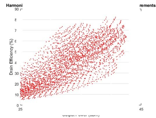
The Maximally Efficient Amplifier - Gareth Lloyd Rohde & Schwarz, Munich, Germany - Rohde & Schwarz
TechnicalFeature
• At the fundamental frequency, the                                                  components and is sinusoidal. Pow-                        the mechanisms for reducing the
  signal current through the device                                                  er is dissipated by the device when                       wasted power in a tuned amplifier.
  passes solely to the intended load                                                 a current (id) flows through it with a                    These mechanisms relate only to the
  impedance (Zload), creating a volt-                                                voltage (vd) across it and where the                      device itself, not to external modu-
  age across the device and load.                                                    current and voltage overlap during                        lating circuitry such as harmonic
• Harmonic       currents    flowing                                                 the waveform cycle. For a class A                         terminations or modulators. Three
  through the device are short                                                       amplifier, the simplest case, Figure 2                    base mechanisms can enhance the
  circuited through the highpass                                                     shows the power dissipation versus                        efficiency of a single-ended ampli-
  filter, as any harmonic currents                                                   time at three power levels. As the                        fier: waveform engineering, supply
  flowing in the device “see” zero                                                   output power reduces, the power                           modulation and load modulation.
  impedance and do not create                                                        dissipated waveform tends to a con-                           Waveform        Engineering—The
  any voltage.                                                                       stant value. At higher output power,                      shape of the voltage and/or current
  The voltage across the device                                                      the dissipated power reduces. The                         waveform is modified, which is what
comprises only DC and fundamental                                                    power consumption is constant in all                      happens when passing through the
                                                                                                        cases, and the pow-                    class A to C continuum. Harmonic
         Current Through

                                                                                                        er dissipated is the                   content is introduced into the cur-
                           2                           2                            2                   total area under the                   rent, modifying its waveform, in a
                           1                           1                            1
                                                                                                        power dissipation                      predictable but restricted way.1 Al-
                                                                                                        curve. In the case of                  ternatively, the ratio of the current’s
                                                                                                    1 this class A ampli-                      harmonic content may be modified
                           0                           0                            0
                               0       0.5     1           0           0.5      1     0     0.5
                                                                                                        fier, the amount of                    by injecting harmonics from either
          Voltage Across

                                                                                                        power dissipated                       the input side or output side. For the
                           2                           2                            2
                                                                                                        (wasted) decreases                     current’s harmonic content to affect
                           1                           1                            1                   as output power                        the voltage waveform, a non-zero im-
                           0                           0
                                                                                                        level      increases,                  pedance must be present at that har-
                                                                                    0
                               0       0.5     1           0           0.5      1     0     0.5     1 from (a) to (c).                         monic frequency. In the limiting case,
                                                                                                                                               both current and voltage waveforms
 Power Dissipation

                           2                           2                            2
   Instantaneous

                                                                                                                      EFFICIENCY               are square waves and antiphase. As
                           1                           1                            1                                 ENHANCEMENT              one of them is zero at any instant in
                                                                                                                         How will effi-        time, the power dissipation is zero.
                           0                           0                            0                                 ciency     enhance-      This zero dissipation applies at least
                               0       0.5     1           0           0.5      1        0            0.5         1
                                                                                                                      ment mechanisms          to the device, but it could just be
                           (a)         Time            (b)             Time             (c)           Time
                                                                                                                      improve the ener-        shifted elsewhere in the system.
                                                                                                                      gy efficiency? Con-          Supply Modulation—The aver-
  Fig. 2 Class A amplifier waveforms at low (a), medium (b)
                                                                                                                      sider     classifying    age or envelope supply voltage
and high (c) output power.
                                                                                                                                               across the device, Vsupply, is modi-
                                                                                                                                               fied. With a perfect device, Vsupply
                                                                                                                                               is the root-mean-square value of the
       Current Through

                               2                               2                              2                             2
                                                                                                                                               voltage waveform, set so the mini-
                                                                                                                                               mum value of vd reaches zero.
                               1                               1                              1                             1
                                                                                                                                                   Load Modulation—The Zload
                                                                                                                                               presented to the device at the fun-
                               0                               0                              0                             0
                                   0     0.5       1               0      0.5       1             0         0.5       1         0   0.5    1   damental frequency is modified,
                                                                                                                                               ideally so the voltage (vd) swings
                                                                                                                                               from 0 to 2 times the supply.
       Voltage Across

                               2                               2                              2                             2                      Figure 3 illustrates these mecha-
                                                                                                                                               nisms using a class B waveform as
                               1                               1                              1                             1                  the reference. The class B current
                                                                                                                                               waveform is half sinusoidal, com-
                               0                               0                              0                             0                  pared to fully sinusoidal for class
                                   0     0.5       1               0      0.5       1             0         0.5       1         0   0.5    1
                                                                                                                                               A operation. The fundamental cur-
                               1                           1                                  1                             1                  rent is equal in both classes A and
                                                                                                                                               B when the peak-to-peak current
Power Dissipation
  Instantaneous

                                                                                                                                               variation is equal. The reason for us-
                           0.5                         0.5                               0.5                              0.5                  ing a class B waveform as the base-
                                                                                                                                               line is because the efficiency can
                                                                                                                                               be enhanced by all three methods.
                               0
                                   0     0.5       1
                                                           0
                                                                   0      0.5       1
                                                                                              0
                                                                                                  0         0.5       1
                                                                                                                            0
                                                                                                                                0   0.5    1
                                                                                                                                               Class A, on the other hand, cannot
                           (a)          Time           (b)               Time            (c)            Time              (d)       Time
                                                                                                                                               be improved with load modulation
                                                                                                                                               alone: class A power consumption
  Fig. 3 Efficiency enhancement mechanisms compared to a class B waveform at 6 dB                                                             remains constant regardless of the
back-off (a), waveform engineering (b), supply modulation (c) and load modulation (d).                                                         load impedance.
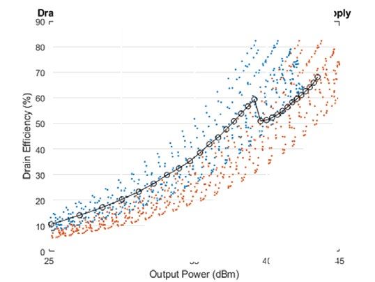
The Maximally Efficient Amplifier - Gareth Lloyd Rohde & Schwarz, Munich, Germany - Rohde & Schwarz
TechnicalFeature
                                                                                                                ply modulation has been applied—
                                                                                                                achieving a quite unexpected result:
       Current Through

                           2               2                 2                2                2                the efficiency at the output power
                                                                                                                back-off of the class A amplifier has
                           1               1                 1                1                1                been maintained at the theoretical
                                                                                                                maximum of 50 percent.
                           0
                            0   0.5    1
                                           0
                                            0      0.5   1
                                                             0
                                                              0    0.5    1
                                                                              0
                                                                               0    0.5    1
                                                                                               0
                                                                                                0    0.5    1
                                                                                                                   The respective efficiencies of the
                                                                                                                five scenarios of Figure 4 are sum-
                                                                                                                marized in Table 1. Note that the
       Voltage Across

                                                                                                                waveforms all have the same output
                           2               2                 2                2                2
                                                                                                                power.
                           1               1                 1                1                1
                                                                                                                POPULAR APPROACHES
                           0               0                 0                0                0
                                                                                                                   Having classified various en-
                            0   0.5    1    0      0.5   1    0    0.5    1    0    0.5    1    0    0.5    1   hancement mechanisms and dis-
                           3               3                 3                3                3
                                                                                                                cussed their effects on theoretical
                                                                                                                amplifier blocks, including advan-
Power Dissipation

                                                                                                                tageous effects from hybrid ap-
  Instantaneous

                           2               2                 2                2                2
                                                                                                                proaches, the discussion moves
                           1               1                 1                1                1                from theory to practice, classifying
                                                                                                                the popular enhancement methods
                           0
                            0   0.5    1
                                           0
                                            0      0.5   1
                                                             0
                                                              0    0.5    1
                                                                              0
                                                                               0    0.5    1
                                                                                               0
                                                                                                0    0.5    1
                                                                                                                according to the mechanisms they
                         (a)    Time       (b)    Time       (c)   Time       (d)   Time       (e)   Time
                                                                                                                use (see Figure 5). Using a Venn
                                                                                                                diagram for classification helps
                                                                                                                identify where additional schemes
  Fig. 4 Class A amplifier efficiency at 6 dB back-off (a) enhanced by waveform
                                                                                                                are complementary and may further
engineering (b), supply modulation (c), load modulation (d) and an unexpected
improvement using a counter-intuitive hybrid (e).                                                               improve efficiency.
                                                                                                                   For example, the Doherty ampli-
                                                               waveform      engi-
                                                 TABLE 1       neered to add the
                                                                                                                fier, which applies load modulation
                                                                                                                to its constituent amplifiers, can be
           APPROACHES TO INCREASE CLASS A                      required harmon-
                    AMPLIFIER EFFICIENCY                                                                        improved by adding supply modu-
                                                               ics? For example, it                             lation, especially to the main chan-
                               % Efficiency at 6 dB Back-Off might be operating                                 nel, and/or waveform engineering,
          Configuration                                        close to its upper
                                  (25% of Rated Power)                                                          by modifying the design to incor-
                                                               frequency limit and                              porate class F-1 operation, for ex-
         Class A Baseline                   12.5
                                                               cannot support the                               ample.
      Waveform Engineered                                      harmonic currents.
                                            39.3
      (Equivalent to Class B)                                  Supply modulation                                Harmonic Load-Pull
        Supply Modulation                   25.0               in Fig. 4(c) could                                  A bottleneck is getting real world,
                                                               be used, although                                practical devices to use the theoret-
         Load Modulation                    12.5               combining it with                                ical enhancements. For example, a
 Anti-Load & Supply Modulation              50.0               load     modulation                              typical GaN device may be sensitive
                                                               would be coun-                                   to efficiency enhancement by load
                                            terproductive. Load modulation in-                                  modulation over a 5–10:1 imped-
Class A Case Study                          creases the peak-to-peak voltage,                                   ance range. However, when used as
   One of the goals of this article         decreasing the range where sup-                                     the main device in a Doherty archi-
is to illustrate efficiency enhance-        ply modulation could be deployed.                                   tecture, it is typically exploited only
ment mechanisms so they can be              Turning the problem around, if load                                 over a 2–3:1 range. The Doherty
used optimally. The class A case is         modulation degrades the effective-                                  scheme will fail to maximize the po-
not a lost cause. Figure 4 shows the        ness of supply modulation, what if                                  tential performance of the device.
voltage, current and dissipation for        “unload” modulation were applied?                                      Harmonic load-pull measure-
a class A amplifier, illustrating that      Instead of maximizing the load im-                                  ments over a range of bias condi-
waveform engineering and supply             pedance to maximize peak-to-peak                                    tions make it possible to establish
modulation enhance efficiency, but          voltage, minimize the load imped-                                   the maximum performance enve-
load modulation does not. Wave-             ance to minimize the peak-to-peak                                   lope for the device technology.
form engineering can convert the            voltage and then use supply modu-                                   Load-pull data can be obtained us-
class A sinusoidal current into the         lation. This is the case shown in Fig-                              ing various setups, such as Maury
class B case of the half sinusoid           ure 4(e), the “anti-load modulation +                               Microwave’s harmonic load-pull
in Fig. 4(b). Referring to Figure 3,        supply modulation” case. The peak-                                  test bench with an R&S ZNA vector
class B efficiency could now be en-         to-peak values of current and voltage                               network analyzer (see Figure 6). By
hanced with load modulation.                have been completely reversed from                                  comparing harmonic load-pull mea-
   What if the device could not be          the load modulation case, and sup-                                  surement data with the theoretical
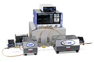
The Maximally Efficient Amplifier - Gareth Lloyd Rohde & Schwarz, Munich, Germany - Rohde & Schwarz
TechnicalFeature
                                                                                                        power approaches 15 dB.
                    Load                                                          Supply                    For a Doherty amplifier, the (sim-
                                  Doherty-Main
               Modulation                                                         Modulation            plified) relationship between output
                                Doherty-
                                Auxiliary         Multilevel                                            power and impedance is defined by:
                                                 Outphasing
                             Outphasing                             Envelope                            iaux = 2imain-1, where imain, the nor-
                                                                  Tracking (ET)
                              Load                                                                      malized output current from the
                           Modulation
                            Balanced
                                                                                                        main transistor, varies from 0 to 1.
                                                                                                        iaux = 0 where iaux < 0. iaux is the nor-
                                    Doherty                    Class                                    malized output current of the auxil-
                                   + Class F-1                 F + ET                                   iary device.
                                                   Class F
                                                                                                            The normalized impedances pre-
                                                                                                        sented to the main and auxiliary
                                            Switched-Mode                                               transistors are
                                                Power
                                              Amplifiers                                                Zmain = 2 – iaux/imain and Zaux = 1/
                                                                                                        (iaux/imain), respectively.
                                             Waveform
                                            Engineering                                                     The output power contributions
                                                                                                        from the constituent amplifiers are
   Fig. 5 Efficiency enhancement mechanisms, their hybrids and possible areas for
                                                                                                        given by
further improvement.
                                                                                                        Pmain = imain2 × Zmain and Paux =iaux2
                                                                 Thus there are several ways to use     × Zaux
                                                              the data from a rigorous and repeat-
                                                              able setup for measuring load-pull.           In this Doherty example, a the-
                                                              One is to create characterization and     oretical output current relation-
                                                              architectural databases for cross-        ship is used, although the equa-
                                                              referencing device performance with       tion relating iaux and imain can be
                                                              various circuit architectures and         changed, using a square law auxil-
                                                              enhancement methods: Doherty,             iary relationship for example, where
                                                              load modulated, balanced, outphas-        iaux=√imain. The impedance values
                                                              ing, etc. The design flow of Figure       Zmain and Zaux may be scaled to any
 Fig. 6 Maury          load-pull test system                 7 shows possible steps for setting        value in the dataset. In this case,
using the R&S®ZNA VNA.                                                                                  10 Ω is used as a multiplier prior to
                                                              up and using a look-up table for
                                                              assessing device performance and          the look-up operation; fixed values
performance of a selected high ef-                            enhancement techniques. To illus-         for the harmonic impedances have
ficiency technique, the performance                           trate the concept, a commercially         also been chosen prior to look-up.
gap can be quantified, answering                              available Wolfspeed GaN transis-          With the definition for output pow-
the question of the difference be-                            tor (CG2H40010) was characterized         er and impedance for the main and
tween what has been built and the                             at a fundamental frequency of 2           auxiliary devices, the look-up-table
performance limit. Alternatively,                             GHz and a bias current of 100 mA          operation is performed on the mea-
if the device is assumed to be the                            using a Maury harmonic load-pull          surement data to extract the drain
bottleneck, the harmonic load-                                test bench. The measurement data          efficiency, with interpolation of the
pull measurement data enables a                               was analyzed to understand device         measurements used to determine
scheme to be designed to maximize                             performance in a Doherty amplifier,       intermediate values.
its potential, using the optimal en-                          then compared with the maximum                With the output power and drain
hancement mechanisms in the cor-                              performance possible from the de-         efficiency for the main and auxiliary
rect proportions.                                             vice. Figure 8 shows the output           known individually, the compos-
                                                                               power and drain ef-      ite power consumption and out-
                                                                               ficiency as the input    put power can be calculated. The
       Perform Harmonic Load-Pull
  (Efficiency Pout) = f(Vsupply, Zf0, Zfn)
                                             Create Database of Architectures
                                                                               power, fundamental       simulated output power and drain
                                                (Zf0, Zfn, Vsupply) = f(Pout)
                                                                               and harmonic ter-        efficiency of the Doherty power am-
                                                                               minations and sup-       plifier is plotted in Figure 9, using
         Add to Device Database                Add to Architecture Database
                                                                               ply voltages were        the measured data for the look-up
                                                                               swept. This scatter      operation. Because two devices are
          Use Lookup Table to Extract Device Performances in Different         plot provides the        used in a Doherty, the output power
                 Architectures (Doherty, Outphasing, Class F, ET)
                                                                               performance limit        capability is 3 dB higher, so a second
                                                                               of a single-ended        scatter plot of the measured data,
          Compare Opportunity vs. Cost. Select Device and Application                                   increased by 3 dB, is included. The
                                                                               device; to achieve
                                                                               drain       efficiency   second scatter plot represents the
                                      Implement                                greater than 50 per-     performance limit. The load modu-
                                                                               cent, the dynamic        lation mechanism offered by the
 Fig. 7 Process flow to achieve the best device-architecture range of the output                       Doherty architecture—the limited
pairing.
TechnicalFeature
                         90                                                                          90

                         80                                                                          80

                         70                                                                          70

                                                                              Drain Efficiency (%)
                                                                                                     60
  Drain Efficiency (%)

                         60

                         50                                                                          50

                         40                                                                          40

                         30                                                                          30

                         20                                                                          20
                                                                                                                            • Fixed (Znf0, Vds)
                         10                                                                          10                     • Fixed (Znf0, Vds) + 3 dB
                                                                                                                              Doherty
                          0                                                                          0
                           25   30           35           40            45                            25   30           35            40                 45
                                     Output Power (dBm)                                                         Output Power (dBm)

  Fig. 8 Single-ended GaN transistor drain efficiency and
                                                                                Fig. 9 Calculated drain efficiency and output power vs.
                                                                             measured drain efficiency and output power with fixed supply
output power vs. swept input power, supply voltage (10,                      voltage and harmonic impedances.
20 and 28 V) and fundamental, second and third harmonic
impedances.
                                                                                This model for the Doherty could be more sophis-
                         90
                                                                             ticated, including other effects without detracting from
                         80                                                  the basic flow. Alternatively, it could be that a different
                                                                             enhancement scheme offers a greater benefit for the
                         70                                                  device, whether tailored from the ground up or off-the-
                                                                             shelf. Other concepts can be analyzed using different
 Drain Efficiency (%)

                         60
                                                                             equations and look-up parameters. For example, using
                         50                                                  the outphasing architecture, the impedances presented
                         40
                                                                             to the voltage source devices are derived from the co-
                                                                             tangent of the inverse sine of the output amplitude.1
                         30
                                                                             CONCLUSION
                         20
                                                                                A classification of efficiency enhancement mecha-
                         10                      • Measured Possible         nisms has been proposed, and their effects on class A
                                                   Calculated Doherty        and class B amplifiers described, allowing for comple-
                         0                                                   mentary mechanisms to be identified.
                          25    30           35           40            45
                                     Output Power (dBm)                         It is suggested that harmonic load-pull measure-
                                                                             ments, over a range of supply voltages, which are anal-
  Fig. 10 Calculated drain efficiency and output power vs.                  ogous to the mechanisms, can fully extract the perfor-
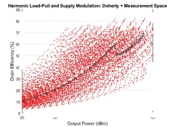
measured drain efficiency and output power showing full                      mance potential of the device.
supply voltage and harmonic impedance variations.                               From those measurements, performance of the de-
2:1 modulation range presented to the dominant main                          vice in a range of architectures (e.g. Doherty) can be
device, combined with the arbitrary impedance trajec-                        predicted.
tory selected for this illustration—does not fully exploit                      State-of-the-art devices, such as the Wolfspeed de-
the device’s capability for load modulation. The device                      vice illustrated in this article, are capable of much better
is, in effect, being driven in first gear. While the measure-                performance than state-of-the-art architectures.
ment space indicates a capability of 8 dB dynamic range                         Therefore, that designing a “good enough” supply-
achieving at least 50 percent drain efficiency, the Doherty                  modulated harmonic load-pull, appropriate for the ap-
only manages to exploit about 5 dB of that range, also                       plication at hand, should be a goal for those responsible
missing a couple of dB of saturated output power. The                        for developing power efficient RFFEs.n
same extracted Doherty performance plotted on the en-
                                                                             ACKNOWLEDGMENT
tire measurement space, including the full harmonic and
supply variations, is shown in Figure 10. For efficiency of                     The author would like to thank Maury Microwave for
50 percent or greater, the output power dynamic range                        providing the measurement data.
is now nearly 18 dB with the addition of the auxiliary tran-
                                                                             Reference
sistor’s 3 dB contribution. Clearly the performance of the                   1.		Cripps, S. C., “RF Power Amplifiers for Wireless Communica-
Doherty in this example would benefit from the addition                          tions,” 2006, Artech House, Norwood, Mass., Chapter 3.
of supply modulation and/or waveform engineering.
You can also read