A method for EMCCD multiplication gain measurement with comprehensive correction
←
→
Page content transcription
If your browser does not render page correctly, please read the page content below
www.nature.com/scientificreports
OPEN A method for EMCCD
multiplication gain measurement
with comprehensive correction
Li Qiao*, Mingfu Wang & Zheng Jin
In order to improve the image quality, it is imperative to conduct the non-uniformity correction of
EMCCD, for which the measurement accuracy of the internal electron multiplication gain of each
channel is a prerequisite within multi-channel output EMCCD. It is known that the smaller the image
standard deviation of each channel, the better the image uniformity, and the closer the calculated
multiplier gain is to the real value. In order to minimize the influence of non-uniformity of background
between pixels and light response existing in traditional measurement, a comprehensively modified
EMCCD multiplication gain measurement is proposed after the working principle of EMCCD is
described. The output images of the camera working in the normal CCD mode and EMCCD mode
are corrected comprehensively through this method. The experimental results show that after the
comprehensive correction, the standard deviation of the output image of each channel within the
camera decreases to about one third of the original when the camera works in the normal CCD mode,
while it decreases to about one fifth of the original when the camera works in the EMCCD mode, the
signal stability is significantly improved, and the measured multiplier gain of each channel is closer to
the true value of the detector, which proves the effectiveness of the proposed method.
EMCCD is known as electron multiplying charge coupled device. Compared with the traditional CCD, EMCCD
adds an electron multiplier register (EMR) between the readout register and the readout a mplifier1–3. The EMR
can amplify the weak electrical signal exponentially, so as to achieve the purpose of multiplication. This process
can greatly improve the detection sensitivity of EMCCD, making it one of the most widely used high-end detec-
tors in the field of low-light imaging fields.
Non-uniformity correction of EMCCD is the key to improve image quality. There are many factors affect-
ing the non-uniformity of common CCD, such as the non-uniformity of background and light response, dark
current, device aging, etc. The non-uniformity of EMCCD includes not only the non-uniformity component of
common CCD, but also the non-uniformity caused by multiplication gain: (1) non-uniformity between different
channels. The multi-tap output structure adopted by EMCCD chip can improve the maximum output frame rate
of the detector, which, simultaneously, will also introduce the non-uniformity caused by the difference of real
multiplication gain between image channels; (2) non-uniformity between pixels within channel. The multiplica-
tion of photo-generated charge in EMCCD’s electron multiplier register is a random process, which brings in
discrepancies of multiplication gain between pixels and introduces non-uniformity. When the multiplication
gain increases, the introduced non-uniformity often increases as well, which will even be the main component
of the non-uniformity of EMCCD under the extremely weak light imaging condition. In the process of true mul-
tiplier gain measurement, the effective signal is both affected by the non-uniformity of background and optical
response, which leads to the difference between the actual measurement and the true multiplier gain. At present,
the research on non-uniformity correction mainly focuses on infrared imaging and common CCD imaging4–11.
The related scientific research of EMCCD mainly concentrates on the application of weak light imaging in
astronomical observation12–19, biomedical20–26 and other fields. There are few literatures on the non-uniformity
characteristics of EMCCD imaging and its correction. The comprehensive correction method proposed in this
paper can greatly reduce the influence of background non-uniformity and optical response non-uniformity on
the effective signal for calculating the multiplier gain. After comprehensive correction, the standard deviation of
the output image of the 8-channel EMCCD detector CCD220 from e2v company is significantly decreased, and
the image quality is significantly improved, the real multiplier gain of each channel of EMCCD can be obtained
more accurately from the comprehensively corrected image.
Institute of Optics and Electronics, Chinese Academy of Sciences, Chengdu 610209, Sichuan, China. * email:
834988645@qq.com
Scientific Reports | (2021) 11:6058 | https://doi.org/10.1038/s41598-021-85511-z 1
Vol.:(0123456789)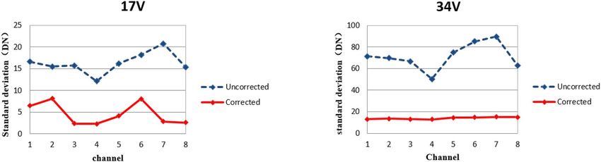
www.nature.com/scientificreports/
Figure 1. Schematic diagram of EMCCD structure.
Mechanism of EMCCD
The internal structure of EMCCD is mainly composed of imaging, store, read-out register, multiplier register,
readout amplifier and back-end c ircuit2. Photo generated charge is formed when the imaging area is irradiated
by the external light, the transfer process is shown in Fig. 1. Firstly, the photo generated charge will be transferred
to the storage area continuously within the specified exposure time and then to the readout register sequentially,
where the photo generated charge will be sent to the multiplication register for exponential multiplication and
then to the readout amplifier and the back-end circuit for processing, and finally the image will be output.
The electron multiplier register is a multi-stage multiplier register. The real multiplication gain of photo-
generated charge in the electron multiplier register is shown in Eq. (1)27:
G = (1 + r)N (1)
In this equation, G is the number of electrons output after a single electron is amplified by the multiplier reg-
ister, that is, the true multiplier gain (no unit). N is the number of electron multiplication units in the multiplier
register (no unit), which is 520 for CCD220. r is the additional multiplication coefficient (r ≥ 0, no unit). When
r = 0, the camera works in normal CCD mode; when r > 0, the camera works in EMCCD mode. The larger the
gain voltage of the multiplier register, the greater r and G and vice versa.
Measurement of multiplication gain based on comprehensive correction
Principle of correction. The true multiplier gain of the multiplier register is the ratio of the signal after
multiplication to the one before multiplication. The calculation formula is as follows:
S(gain) S bright, gain − S(dark, gain)
G= =
(2)
S(no gain) S bright, no gain − S(dark, no gain)
In this equation, G is the true multiplication gain of the multiplier register; S bright, gain is the
bright field
signal after multiplication; S(dark, gain) is the dark field signal after multiplication; S bright, no gain is the bright
field signal without multiplication; S(dark, no gain) is the dark field signal without multiplication; S(no gain) is
the original input signal of the multiplier register; S(gain) is the output signal after multiplication. The accuracy
of G is directly affected by S(gain) and S(no gain). Therefore, it is necessary to comprehensively correct the input
and output signal of the multiplier registers in advance according to the existing non-uniformity characteristics
of the background and the light response between pixels. The corrected multiplier gain is calculated as follows:
′
′ S (gain) f S bright, gain − f S(dark, gain)
G = ′ =
(3)
S (no gain) f S bright, no gain − f S(dark, no gain)
G is real multiplier gain calculated after comprehensive correction; f is the comprehensive correction function
′
of EMCCD output image.
Determination of comprehensive correction function. Non‑uniformity composition. The dark field
image is the output of camera under condition of no light (no photoelectric conversion), while the bright field
image is the one under the condition of light (photoelectric conversion). The background image is the dark field
image when the camera is set to the minimum exposure time. The light input of the camera is adjusted by con-
trolling the exposure time when the brightness of the light is kept constant. The gray value of bright field image
is the sum of those of background image and light response signal, as shown in formula (4)
imagedark0 (i, j) + k(i, j) ∗ A ∗ texp + b(i, j) = imagebright (i, j) (4)
In this equation, i, j is the ith row and jth column of the pixel in the image; A (unit: photons/s) is the coef-
ficient related to the brightness of the light source; texp is the exposure time; imagedark0 is the background image;
Scientific Reports | (2021) 11:6058 | https://doi.org/10.1038/s41598-021-85511-z 2
Vol:.(1234567890)www.nature.com/scientificreports/
k , b is the slope and intercept of the light response curve of a single pixel respectively (hereinafter referred to
as the light response coefficient); photons is the light input of the camera. The difference of gray value between
pixels within background image incurs the background non-uniformity of camera, while the difference of light
response coefficient k and b between pixels brings in the non-uniformity of light response. Therefore, the back-
ground non-uniformity and light response non-uniformity are introduced into the bright field image. The light
response signal is the difference between the bright field image and the background image, which effectively
removes the non-uniformity of the background image and only retains the non-uniformity of the light response.
By determining the corresponding background gray value and light response coefficient of each pixel, the output
bright field image can be comprehensively corrected.
Determination of correction coefficient. The mean image can effectively eliminate the influence of random
noise, and its calculation formula is as follows:
n
imagem (i, j)
imageave (i, j) = m=1 (5)
n
In this equation, imagem is a single image; n is the number of collected images; imageave is the calculated
mean image.
The background image imagedark0 is obtained by fitting the camera under the dark condition, setting the
exposure time to the minimum, collecting various dark field images, and then calculating the mean image
according to formula (5).
The brightness of the light source is remained unchanged and multiple bright field images are captured at m
exposure times texp, then the bright field mean image is calculated. By subtracting m background mean images
from bright field mean images, the light response signal of each pixel imagediff can be obtained. Finally, the light
response coefficient of a single pixel can be obtained by linearly fitting as shown in formula (6)
imagediff i, j = k i, j ∗ A ∗ texp + b(i, j) (6)
In this equation, k ∗ A and b are the fitted light response coefficients.
The following can be drawn from formula (4):
imagebright i, j − image (i, j) − b(i, j)
texp =
dark0 (7)
k i, j ∗ A
In this equation, imagebright is the bright field image to be corrected, imagedark0 is the background image
(equivalent to dark field image).
Comprehensive correction. The mean value of the whole image is shown in formula (8):
row col
i=1 j=1 image(i, j) (8)
aveimage =
row ∗ col
In this equation, row, col are the total number of rows and columns respectively, image is the single image;
aveimage is the mean value of the whole image.
According to formula (8), the mean values of the background image imagedark0 i, j , light response coefficients
k i, j ∗ A and b i, j are calculated to be imagedark0_ave , kave ∗ A, bave , respectively.
The bright field image after comprehensive correction can be calculated from its composition as follows:
imagemodify i, j = imagedark0_ave + kave ∗ A ∗ texp (i, j) + bave (9)
Apply formula (7) into (9), the following results can be obtained:
imagemodify i, j = ktotal i, j ∗ imagebright i, j + btotal i, j (10)
kave ∗ A
ktotal i, j =
(11)
k i, j ∗ A
kave ∗ A ∗ imagedark0 i, j + b i, j
(12)
btotal i, j = imagedark0_ave + bave −
k i, j ∗ A
In formulas (10)–(12), imageave_dark0 is the mean value of the whole image of imagedark0; imagemodify is the
image after comprehensive correction.
The comprehensive correction function corresponding to function f in formula (3) is shown in Eqs. (13–15):
(13)
Y i, j = ktotal i, j ∗ X i, j + btotal i, j
Scientific Reports | (2021) 11:6058 | https://doi.org/10.1038/s41598-021-85511-z 3
Vol.:(0123456789)www.nature.com/scientificreports/
Number Factor Symbol
1 Background image imagedark0
2 Average background image imagedark0_ave
3 Slope of light response curve k∗A
4 Average slope of light response curve kave ∗ A
5 Intercept of light response curve b
6 Average intercept of light response curve bave
Table 1. Correction factors to be determined.
kave ∗ A
ktotal i, j =
(14)
k i, j ∗ A
kave ∗ A ∗ imagedark0 i, j + b i, j
(15)
btotal i, j = imagedark0_ave + bave −
k i, j ∗ A
In this equation, X is the original image to be corrected; Y is the image after comprehensive correction.
Measurement procedure. According to formulas (14) and (15), it is necessary to determine six factors in
Table 1 for the comprehensive correction of the original image of the camera. The more the number of collected
images, the smaller the random error of the mean image. Therefore, 100 background images were collected to
calculate imagedark0 in this paper according to formula 5, then imageave_dark0 can be obtained by substituting
imagedark0 into formula (8). The process of obtaining the light response coefficients of the pixels in the ith row
and jth column is shown in Fig. 2. As the light response coefficients are obtained from linear fitting, the more
sampling points, the more accurate the result is. In this paper, 20 exposure time points are used for linear fitting.
The slope k ∗ A and intercept b of the light response curve can be calculated after the operation for all pixels as
shown in Fig. 2, the mean value of slope kave ∗ A and intercept bave can be obtained from formula (8).
After the parameters in Table 1 are calculated, the comprehensive correction coefficient ktotal , btotal are
obtained by substituting them into formulas
(14) and (15). Finally, ktotal , btotal and the original output image
are substituted into formula (13) as X i, j to get the camera output image with comprehensive correction. By
sending the light field image and dark field image corrected into formula 2, the final true multiplier gain value
with comprehensive correction can be calculated.
Experimental results
The CCD220 chip of British e2v company possesses sub-electron readout noise capability and excellent spectral
response characteristics, which is a typical high frame rate EMCCD chip used in adaptive optics. CCD220 chip
adopts 8-channel parallel output mode, which can improve the maximum output frame rate of the camera. The
resolution of the final output image is 240 × 240, and it is composed of eight channels. The non-uniformity of the
multiplication gain between channels will directly incur the non-uniformity of the original output image, which
produces eight distinct regions. In this paper, CCD220 chip is taken as an example to compare the calculation
results of the traditional method with the new proposed one.
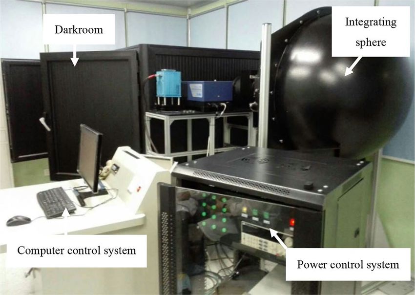
Experimental equipment and parameters. Figure 3 shows the hardware equipment of this experi-
ment, which is composed of integrating sphere, darkroom, power control system and computer control system.
The camera is installed on a special bracket in the darkroom, and the CCD220 is facing the center of the inte-
grating sphere light outlet. The distance between the target surface of the detector and the light outlet of the
integrating sphere is about 1.2 m. The integrating sphere has four levels of transmittance of 100%, 10%, 1% and
0.1%, which can provide the normal light environment for the camera when it works in the non-multiplication
gain mode and the weak light environment when it works in the high multiplication gain mode.
According to the chip manual, CCD220 works in the normal CCD mode when the gain voltage is 17 V, and
the true multiplier gain G is 1, which raises exponentially with the increase of the gain voltage. Therefore, the
output image of the camera was measured in experiment when the gain voltage was 17 V (with the multiplier
register off) and 34 V (with the multiplier register on). The relevant test parameters are shown in Table 2.
Experimental result. Comparison of images. Figures 4 and 5 show the original output image and the
one after the comprehensive correction obtained by CCD220 detector when the gain voltage is 17 V and 34 V,
respectively.
The output image of CCD220 consists of 8 channels, namely eight rectangular regions in the single image as
shown in Figs. 4 and 5. The four regions in the upper half are named channel 1–4, similarly the four in the lower
half are named channel 5–8. It can be seen from the above figure that the uniformity of the output image in a
single channel has been significantly improved after comprehensive correction, the most intuitive difference is
that there is a noticeable bright spot in the center of the whole image before correction but it nearly dies away
after correction.
Scientific Reports | (2021) 11:6058 | https://doi.org/10.1038/s41598-021-85511-z 4
Vol:.(1234567890)www.nature.com/scientificreports/
Start
Keep the brightness of
the light source constant
Pick 20 exposure times (texp(i),i=1~20) uniformly
distributed in the linear response of the camera
i=1
Set exposure time texp(i)
Capture 100 bright field images
Store the mean image of 100
bright field images as imagebright-i
imagediff_i=imagebri ght_i-imageave_dark0
iŏ20 Y i=i+1
N
Take the texp as x-axis and the gray values
of the i-th row and j-th column in the
imagebright_i as y-axis for linear fitting
Calculate the linear fitting parameters
of the pixels in the i-th row and j-th
column to be k(i,j)*A and b(i,j)
End
Figure 2. Calculation flow chart of light response coefficient of single pixel.
Statistical comparison. The internal standard deviation of single channel image is calculated as follows:
row col
2
i=1 j=1 (image i, j − imageave ) (16)
std image =
row ∗ col − 1
In this equation, std image is the standard deviation of the single channel image.
Scientific Reports | (2021) 11:6058 | https://doi.org/10.1038/s41598-021-85511-z 5
Vol.:(0123456789)www.nature.com/scientificreports/
Figure 3. Integrated test platform of EMCCD.
Current of integrating sphere (A) 0.8
Transmittance of integrating sphere 100%
Exposure time (ms) 0.5
Voltage of gain register (V) 17, 34
Table 2. EMCCD working parameters.
Figure 4. Comparison of CCD220 output image before and after correction when the gain register voltage is
17 V.
Figure 5. Comparison of CCD220 output image before and after correction when the gain register voltage is
34 V.
Scientific Reports | (2021) 11:6058 | https://doi.org/10.1038/s41598-021-85511-z 6
Vol:.(1234567890)www.nature.com/scientificreports/
Standard deviation (DN)
Gain voltage
(V) Channel 1 Channel 2 Channel 3 Channel 4 Channel 5 Channel 6 Channel 7 Channel 8 Total image
17 16.59 15.50 15.72 12.10 16.15 18.21 20.77 15.37 16.30
34 71.35 69.67 66.63 50.25 74.95 85.28 89.81 62.93 71.36
Table 3. Standard deviation of original 8-channel image.
Standard deviation (DN)
Gain voltage
(V) Channel 1 Channel 2 Channel 3 Channel 4 Channel 5 Channel 6 Channel 7 Channel 8 Total image
17 6.50 8.11 2.35 2.33 4.16 8.09 2.82 2.63 4.62
34 13.07 13.61 13.18 12.83 14.48 14.65 15.20 14.97 14.00
Table 4. Standard deviation of 8-channel image after comprehensive correction.
Figure 6. Standard deviation of CCD220 8-channel image before and after correction under different gain
voltages.
In this experiment, the integrated test platform of EMCCD adopts the integrating sphere as the system light
source, with the brightness uniformity of the light outlet more than 97% and the brightness stability less than
0.05% within 30 min. Ideally, the standard deviation of the effective signal for calculating the multiplier gain
should be 0 DN, namely the smaller the standard deviation of the effective gain signal is, the more stable the signal
is, and the closer the calculated multiplier gain is to the true value. Tables 3 and 4 show the 8-channel standard
deviation of the original image and the one after comprehensive correction, respectively, when CCD220 gain
register voltage is set to be 17 V and 34 V.
Figure 6 shows the trend of standard deviation of 8-channel effective signal when the gain voltage of CCD220
is 17 V and 34 V, respectively. The blue dotted line represents the uncorrected image while the red solid line
represents the comprehensively corrected one. It can be seen from the figure that: (a) when the gain voltage is
34 V, the standard deviation is larger than that when the gain voltage is 17 V. The larger the gain voltage, the
larger the real multiplier gain of the multiplier register. When the effective signal of the image is amplified by the
multiplier gain, the noise of the image is also magnified. (b) Under the same gain voltage, the standard deviation
of the output images of the eight channels is greatly reduced after correction, and the uniformity of the images
in each channel is significantly improved.
As for CCD220, it is necessary to calculate the multiplication gain of each channel separately because of its
special characteristic of 8-channel output at the same time. The non-uniformity of EMCCD output image mainly
includes the non-uniformity of background and light response between pixels, and also the multiplication gain
non-uniformity between channels. The proposed linear correction method in this paper can effectively reduce
the background non-uniformity and the light response non-uniformity between pixels in a single channel. After
the correction, the standard deviation of single channel output is greatly reduced, of which the uniformity is
significantly improved, and the final calculated real multiplier gain of each channel is closer to the real value.
Conclusion
In this paper, a method of EMCCD multiplication gain measurement with comprehensive correction is proposed.
The background non-uniformity and light response non-uniformity of eight channels in the output image of
CCD220 are investigated, and the comprehensive correction coefficient of the effective signal of multiplier gain
in each channel is calculated. The accuracy of the real multiplier gain calculation in each channel of EMCCD
can be improved through the comprehensive correction. It is found that after the correction method described
in this paper the standard deviations of the effective signals of the eight channels are significantly reduced, the
signal stability is significantly improved, and the measured multiplier gain of each channel is closer to the true
Scientific Reports | (2021) 11:6058 | https://doi.org/10.1038/s41598-021-85511-z 7
Vol.:(0123456789)www.nature.com/scientificreports/
value of the detector. This method not only provides a new way to measure the real multiplier gain of EMCCD,
but also provides a theoretical basis for the non-uniformity correction of multi-channel EMCCD.
Received: 14 November 2020; Accepted: 2 March 2021
References
1. Hynecek, J. Charge multiplying detector (CMD) suitable for small pixel CCD image sensors. US Patent No. 5337340. 9 (1994).
2. Zhang, C. L., Chen, Q. & Zhou, B. B. Recent progress toward ultra-sensitivity EMCCD. Infrared Technol. 29(4), 192–195 (2007).
3. Zhang, C. L., Chen, Q. & Yin, L. J. Multiplication model of electron multiplying CCD based on single type of carrier. Acta Arma‑
mentarii 32(5), 380–383 (2011).
4. Liu, C., Jin, W., Chen, Y., Liu, B., Cao, Y., & Liu, X. A self-adaptive non-uniformity correction algorithm for infrared images com-
bined with two-point correction along the rim. in 2010 International Computer Symposium (ICS2010), IEEE (2010).
5. Kim, S. Two-point correction and minimum filter-based non-uniformity correction for scan-based aerial infrared cameras. Opt.
Eng. 51(10), 106401 (2012).
6. Xing, S.X., Zhang, J.J., Sun L.J., Chang, B.K., Qian, Y.S. Two-point Non-uniformity correction based on LMS. Infrared Components
and Their Applications, Proc. SPIE 5640 (2015).
7. Pipa, D. R. et al. Recursive algorithms for bias and gain non-uniformity correction in infrared videos. IEEE Trans. Image Process.
21(12), 4758–4769 (2012).
8. Cao, Y. & Tisse, C. L. Single-image-based solution for optics temperature-dependent non-uniformity correction in an uncooled
long-wave infrared camera. Opt. Lett. 39(3), 646–648 (2014).
9. Rossi, A., Diani, M. & Corsini, G. Bilateral filter-based adaptive non-uniformity correction for infrared focal-plane array systems.
Opt. Eng. 49(5), 057003 (2010).
10. Tendero, Y., Landeau, S. & Gilles, J. Non-uniformity correction of infrared images by midway equalization. Image Process. Line 2,
134–146 (2012).
11. Zheng, N. & Mu, P. G. Illumination uneven image correction algorithm based on improved bilateral filtering. Electron. Meas.
Technol. 42(17), 157–161 (2019).
12. Pool, P. J. et al. Application of electron multiplying CCD technology in space instrumentation. Focal Plane Arrays for Space Tel‑
escopes II, 25 August. Proc. SPIE (2005).
13. Smith, D. R. et al. EMCCDs for space applications. High Energy, Optical, and Infrared Detectors for Astronomy II, 15 June, Proc.
SPIE (2006).
14. Docobo, J. A. et al. EMCCD speckle interferometry with the 6 m telescope: Astrometric measurements, differential photometry,
and orbits. Astronom. J. 140(4), 1078 (2010).
15. Maksimov, A. F. et al. The EMCCD-based speckle interferometer of the BTA 6-m telescope: Description and first results. Astrophys.
Bull. 64(3), 296–307 (2009).
16. Xu, W. J., Zeng, Y., Wei, J. & Gong, H. X. Application of L3VisionCCD in satellite nephograph. Aerosp. Shanghai 23(3), 28–31
(2006).
17. Tulloch, S. M. & Dhillon, V. S. On the use of electron-multiplying CCDs for astronomical spectroscopy. Mon. Not. R. Astron. Soc.
411(1), 211–225 (2011).
18. Sangalli, L. et al. Performance study of the new EMCCD-based all-sky cameras for auroral imaging. Int. J. Remote Sens. 32(11),
2987–3003 (2011).
19. Gong, D. Z., Wang, L. & Lu, X. Detection of faint light EMCCD based on star sensor. Infrared Laser Eng. 36, 534–539 (2007).
20. Muraishi, T. et al. Fast data acquisition in heavy ion CT using intensifying screen—EMCCD camera system with beam intensity
monitor. IEEE Trans. Nucl. Sci. 59(5), 1934–1939 (2012).
21. Donal, J. D., Colin, G. C. Electron-multiplying CCD technology: Application to ultrasensitive detection of biomolecules. Biomedical
Nanotechnology Architectures and Applications, 21 June. Proc. SPIE (2002).
22. Betzig, E. et al. Imaging intracellular fluorescent proteins at nanometer resolution. Science 313(5793), 1642–1645 (2006).
23. Mortensen, K. I. et al. Optimized localization analysis for single-molecule tracking and super-resolution microscopy. Nat. Methods
7(5), 377–381 (2010).
24. Mortensen, K. I. et al. Optimized measurements of separations and angles between intra-molecular fluorescent markers. Nat.
Commun. 6(1), 1–9 (2015).
25. Yildiz, A. et al. Myosin V walks hand-over-hand: Single fluorophore imaging with 1.5-nm localization. Science 300(5628), 2061–
2065 (2003).
26. Ruhnow, F., Zwicker, D. & Diez, S. Tracking single particles and elongated filaments with nanometer precision. Biophys. J. 100(11),
2820–2828 (2011).
27. Robbins, M. S. Determining the multiplication of EMCCD sensor. US Patent No. 8054363 (2011).
Author contributions
Q.L. wrote the main manuscript text and all the figures. Figure 3 of the article "A method for EMCCD multi-
plication gain measurement with comprehensive correction" was obtained by the co-author Mingfu Wang. All
authors reviewed the manuscript.
Competing interests
The authors declare no competing interests.
Additional information
Correspondence and requests for materials should be addressed to L.Q.
Reprints and permissions information is available at www.nature.com/reprints.
Publisher’s note Springer Nature remains neutral with regard to jurisdictional claims in published maps and
institutional affiliations.
Scientific Reports | (2021) 11:6058 | https://doi.org/10.1038/s41598-021-85511-z 8
Vol:.(1234567890)www.nature.com/scientificreports/
Open Access This article is licensed under a Creative Commons Attribution 4.0 International
License, which permits use, sharing, adaptation, distribution and reproduction in any medium or
format, as long as you give appropriate credit to the original author(s) and the source, provide a link to the
Creative Commons licence, and indicate if changes were made. The images or other third party material in this
article are included in the article’s Creative Commons licence, unless indicated otherwise in a credit line to the
material. If material is not included in the article’s Creative Commons licence and your intended use is not
permitted by statutory regulation or exceeds the permitted use, you will need to obtain permission directly from
the copyright holder. To view a copy of this licence, visit http://creativecommons.org/licenses/by/4.0/.
© The Author(s) 2021
Scientific Reports | (2021) 11:6058 | https://doi.org/10.1038/s41598-021-85511-z 9
Vol.:(0123456789)You can also read