RF SOI can Save $Billions in 5G mmWave Network Costs with Efficient PAs
←
→
Page content transcription
If your browser does not render page correctly, please read the page content below
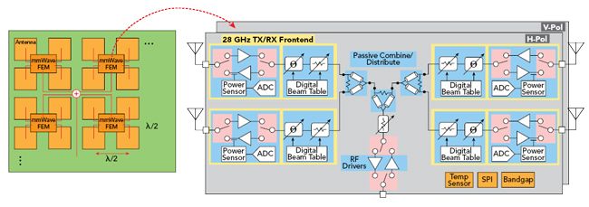
www.microwavejournal.com/articles/33756-rf-soi-can-save-billions-in-5g-mmwave-network-costs-with-
efficient-pas

RF SOI can Save $Billions in 5G mmWave Network
Costs with Efficient PAs
Joe Madden, Mobile Experts; Anirban Bandyopadhyay and Ned Cahoon, GlobalFoundries; Harish
Krishnaswamy, MixComm
April 13, 2020

mmWave 5G networks are a high priority for operators, as the rapid growth of consumer data demand will soon
outstrip the capacity of sub-6 GHz networks forcing American operators to rely on the more difficult mmWave
bands.1 In fact, operators driven by high urban data density deployed more than 85,000 mmWave radio units in
2019. There is no better way to add truckloads of capacity.

However, 5G mmWave deployment has been a bumpy road so far. Operators have discovered that signals above
20 GHz do not behave well. The systems work as expected for line of sight conditions, but non-line of sight
links are not as stable. In field deployment so far, the uplink is the clear limitation. This has always been the
case, in 2G, 3G and 4G systems, as the link budget is usually 2-3 dB weaker for the uplink than the downlink.
This time, however, mmWave field trials have shown more than 15 dB difference between the two link budgets.
5G networks need a closed loop for channel estimation, so both uplink and downlink are necessary. The result
has been unstable performance in the field.

Another major challenge in mmWave comes from high attenuation along the propagation path. Obstacles,
foliage, rainfall or even hands holding the device can add 30 dB of attenuation or more. Phased arrays partially
overcome this limitation via spatial power combining, focusing the signal into narrow steered beams, as well as
spreading the antenna array over a wider area. The benefits of phased arrays have made them the foundation for
5G mmWave deployments, but the lesson here is that the system needs margin, because any small change in the
channel can quickly add 10 dB of path loss.

Today’s 5G mmWave networks are limited by RF power and heat dissipation. The uplink Effective Isotropic
Radiated Power (EIRP) from early user equipment and customer premise equipment (CPE) has been too weak to
provide the necessary link budget margin. At the same time, some devices have shut down during testing due to
overheating.2

The success of mmWave clearly depends on solutions to a few key challenges: 1) Cost associated with limited
range, 2) thermal and electrical power budget and 3) module cost. This article highlights these challenges and
demonstrates how RF SOI based mmWave phased array systems can enable the optimum solution for future
mmWave 5G infrastructure compared to other semiconductor technologies.

BASIC ARCHITECTURE OF THE PHASED ARRAY AND KEY METRICS

Phased arrays consist of multiple antenna elements with phase shifting at each element to steer the beam (see
Figure 1). Phase shifting can occur in either the RF, as depicted in Figure 1, or digital domain. For optimal beam
shape, the spacing of antenna elements in the phased array (lattice spacing) is typically a half wavelength. On-
chip and PCB routing loss are very high at mmWave, so minimizing loss in routing from chip to antenna is
important. As a result, mmWave front-end components (LNA, PA, switch) need to be physically close to each
antenna element. At 28 GHz, λ/2 is 5.4 mm and at 39 GHz, it is 3.9 mm. The lattice spacing constraints and need
for IC/antenna element co-location creates a thermal challenge. This is exacerbated by the low PA efficiency of
first generation solutions. The high peak to average power ration of 5G NR modulation results in a large back-
off from peak power operation, where the PA is inherently inefficient. With transmit efficiencies as low as 5
percent to 10 percent, the great majority of front-end power dissipation goes to heat generation concentrated
within the lattice spacing as opposed to RF signal power. Improving transmit path linear efficiency is thus of
paramount importance for next generation designs.

Figure 1 Large-scale mmWave phased array constructed using tiled 2x2 dual-pol. beamforming
front-end modules (FEM).

The array gain of a phased array is proportional to the number of array elements (N). On the Tx side, the
combination of array gain and additional power per element results in an N2 increase in output power as
compared to a single element. This fundamental property of the phased array enables a trade-off between
semiconductor performance and the size of array needed to meet system requirements. In particular, the N2
reduction in output power per element to achieve the same system EIRP targets makes silicon technologies an
attractive choice for all but the highest power applications.

The minimum requirement is adequate transistor performance (fT and fmax). Designers need a minimum of 5x
and preferably 10x ratio between transistor cutoff frequencies and operation frequency for acceptable gain and
circuit margin at the mmWave carrier frequency. This means that at the 39 GHz 5G band, a 200 GHz fT/fmax is
the minimum acceptable and 400 GHz is preferred. Due to the high losses at mmWave, parasitics of active and
passive elements are critical. Minimizing loss in the metal/dielectric stack is important since transistors must
drive transmission lines at the top metal levels and for efficiency in power combining networks. Thick metal and
dielectric stacks are important in minimizing this loss. Substrate losses are also important; quality factor of
matching networks and transmission line insertion loss improves with higher resistivity substrates. On the Rx
side, transistor NFmin is important for low noise circuits; on the Tx side, breakdown voltage and safe operating
area are paramount for efficient power generation in the PA and for power handling in the antenna switch.

SEMICONDUCTOR TECHNOLOGIES - RF SOI VS CMOS VS GaN

In RF SOI technology, CMOS transistors are built on a top layer of silicon isolated by a buried oxide (BOX)
layer from the silicon substrate. The oxide isolation reduces FET junction capacitance to substrate and improves
FET performance. As a result, transistor fT and fmax in an SOI technology are higher than in a comparable node
planar CMOS technology.
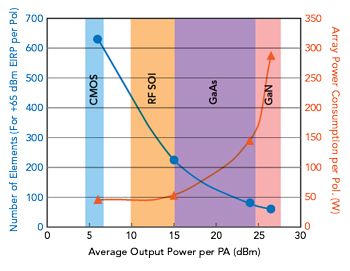
For example, GlobalFoundries (GF) has a 45 nm RF SOI in
production that has been optimized for mmWave performance. NFET
and PFET fT/fmax are 290/330 GHz and 245/300 GHz, respectively.
Metal/dielectric stacks are optimized for mmWave performance and
offer single and dual ultra-thick Cu levels for low loss transmission
lines and combining networks and high Q passives. With the superior
front-end performance and 45 nm logic density, the typical integration
level for solutions based on RF SOI encompasses the PA, LNA, phase-
shifter, and combiner front ends for 4-element and 8-element
beamformers, and may also include mmWave up/down conversion
and RF transceivers. 45 nm logic density enables the integration of
high-speed SPI interfaces with large beam tables containing 1000s of
entries, allowing for agile beamforming for high mobility applications.

A unique advantage of RF SOI technology is the capability to
engineer the substrate for improved RF performance. High resistivity
(>1K ohm-cm) substrates reduce signal loss to the substrate and
improve transmission line loss and Q of matching networks. Higher Q
input matching networks result in lower LNA NF. In addition,
engineered substrates with trap rich layers under the BOX reduce
parasitic conduction mechanisms that otherwise will degrade switch
harmonics and linearity.

RF SOI transistors are fully isolated from each other by the
surrounding oxide. Since the FETs are electrically isolated and there is
no common substrate node as in bulk CMOS, FET’s can be connected            Figure 2 RF-SOI stacked-FET PA
in series (“stacked”) and biased such that the voltage is distributed       concept.
equally across the stack (see Figure 2). Stacking overcomes the low
breakdown voltage limitations of advanced node CMOS since the
breakdown voltage of the stack is the sum of the BVds of the individual transistors in the stack. This is a
significant benefit to front-end circuit performance, resulting in higher PA output power and efficiency and
improved antenna switch insertion loss and power handling. 45 nm RF SOI PAs can deliver peak output power
of 20-23 dBm at 28 GHz with high efficiency (>40 percent PAE). This is in contrast to solutions in advanced
CMOS, where the low breakdown voltage of advanced node FETs results in lower Pout and PAE. The higher
efficiency of RF SOI PAs is important in reducing thermal dissipation and addressing one of the key technology
challenges of 5G arrays.

With 5G NR modulation, the PA will experience peak
RF voltages that are 2x the supply voltage. Accurate
evaluation of transistor degradation under complex 5G
waveforms is important to assure the high reliability
and lifetime requirements of 5G infrastructure are met.
This is best done with PDK tools that seamlessly
integrate reliability models with circuit design and
simulation.

5G mmWave base stations are targeting EIRPs of 60 to
65 dBm. Figure 3 compares the number of elements
required in the Tx phased array to achieve 65 dBm
EIRP, as a function of the average modulated output
power per PA element, and the associated overall Tx
array power dissipation. This figure has been compiled Figure 3 Comparison of semiconductor technologies
using publicly available information on output power       for 5G 28 GHz infrastructure phased-array Tx
and efficiency of PAs implemented in different             applications.
technologies, and factors in the power consumption in
the “plumbing” of the array, namely PA drivers, beamforming circuitry etc. It can be seen that at the lower end
of per PA output power (corresponding to CMOS solutions), the number of array elements becomes very large,
exceeding 500 elements and increasing implementation complexity and cost. On the other hand, at the higher
end of per PA output power (corresponding to GaN), the number of array elements required becomes quite small
(as low as 32 elements). This drives up the overall array power consumption, since the N2 array gain is small,
implying that the EIRP is being achieved through raw output power generation. RF SOI CMOS sits in the
“sweet spot” of complexity versus DC power, as the per PA output power achievable results in manageable array
sizes of 256 elements and low overall Tx array power consumption.

So, there are three general areas where each technology has its strength. CMOS is best for very large arrays,
because it achieves low cost when the power per amplifier is low. RF SOI occupies the “middle ground” where
cost, power efficiency and output power are balanced, such as CPEs and urban mobile infrastructure. GaN
comes into its own where the link is not uplink limited like point-to-point backhaul and at higher frequency
bands (≥60 GHz) where high power per GaN amplifier can be leveraged for smaller array but still maintaining
large point-to-point distance. Because mmWave networks will need to cover a wide variety of terrain and
capacity requirements, it is clear that all three of these solutions will have a place: CMOS phased arrays are well
suited for down link with large number of access points like in a stadium with large numbers of beams and no
need to penetrate building walls or windows. GaN is well suited to long-distance transport network with wider
beams and less steering requirements. RF SOI appears to be best for fixed-wireless CPEs and mobile
infrastructure in urban environments.

DESIGN CHALLENGES FOR RF SOI mmWAVE FRONT-END MODULES

While RF SOI allows for superior Tx and Rx performance, as well as digital integration capability, there is
significant opportunity for innovation in the circuit design as well as the system architecture, both of which are
being actively pursued by companies such as MixComm (in partnership with GF in this case). On the Tx side,
circuit approaches that extract best output power and efficiency from stacked SOI CMOS PAs while maintaining
long-term reliability are critical. Even more important than peak efficiency is the average efficiency under
modulation, with 5G NR waveforms typically dictating ~8 dB of back-off from the 1 dB compression point to
achieve the required 3 percent EVM on the Tx side. In addition to the PA circuit design, the overall front-end
module (FEM) architecture can also have a significant impact on the average system efficiency, and careful
system architecture design and planning is critical.

Digital pre-distortion (DPD) may be employed to extract even better performance from the PAs, but is
complicated by the fact that there will be both systematic and random variations between the PAs of a large-
scale array due to process and temperature variations, as well as amplitude tapering in the beamforming.
Therefore, new array DPD algorithms and PA architectures that are friendly to DPD will enable improved Tx
performance.

The use of DPD is possible for massive MIMO arrays, but it must be a “light” DPD algorithm that consumes
less DC power than is saved in the PA. For very large arrays with low power per PA path, DPD may not be
worthwhile, but for small arrays, at higher RF power levels, DPD may become an important element. One strong
possibility here is to have a DPD algorithm and adaptation engine that is shared among multiple RF paths,
essentially updating the DPD algorithm periodically instead of continuously to save on cost and power devoted
to a single PA path. This approach sacrifices the level of linearization but improves efficiency which is a more
important.

Large-scale phased arrays are subject to amplitude and phase mismatches arising from process, temperature and
package interface variations across the channels of a single FEM chip, as well as across chips. Built-in self-test
and calibration approaches that can compensate for these mismatches are important for the realization of robust
and accurate large-scale arrays. Implementation of these techniques allows for a self-aligning array, which
adapts to field conditions and manufacturing variation to optimize performance in the critical RF front-end.

HOW RF SOI CAN ADDRESS CARRIERS' CHALLENGES

Transmitter output power is perhaps the most fundamental metric of a
radio, and higher output power can be used to improve virtually every
dimension of a mmWave link. Higher output power increases range,
which translates to large cell radius, and consequently fewer base
stations can be deployed, reducing operator CAPEX. Alternatively, for
the same cell radius, it enables higher rates at the cell edge, improving
quality of service. Higher per PA output power can be used by
beamforming algorithms to enable “broad beams,” as opposed to the
conventional narrow “pencil beams,” thus improving robustness in
highly mobile scenarios. Higher per PA output power can also be used       Figure 4 Comparison of median CPE
to reduce BOM cost, as a smaller array is needed to achieve the same       uplink throughput rates for a baseline
EIRP. A smaller array also comes with natural beam broadening and          bulk CMOS-based CPE array and a
associated robustness. Figure 4 compares the median CPE uplink             MixComm GF 45 nm RF-SOI-based
throughput rate of a baseline bulk CMOS-based CPE array with a             CPE array.
DPD 45 nm RF SOI-based CPE array with equal number of antennas.
It can be seen that the higher output power per PA enables significantly superior link budgets, allowing a 2.7x
increase in throughput rate.

WHAT'S THE IMPACT OF AN IMPROVEMENT IN THE mmWAVE AMPLIFIER?

Three challenges will dictate the success of mmWave for mobility: network cost, thermal/power budget and
BOM cost. Our detailed review of semiconductor fundamentals illustrates that RF SOI brings advantages in all
of these areas.

      Higher transmitter power has a huge impact on the financial case for the operators. Adding 3 dB higher
      EIRP to a CPE can save 20 percent of the cost of network deployment, by allowing base stations to be
      deployed farther apart, and also providing higher spectral efficiency. That’s billions of dollars of savings at
      the network level, plus a bonus of higher capacity.
      Almost all radios in the market today are limited by their thermal profile. Improvements to the PA
      efficiency have a direct impact on the real-world EIRP that is achieved. RF SOI sits in a “sweet spot” for
      thermal performance compared with other technologies, allowing for tradeoffs of power, linearity and
      efficiency that far outperform the bulk CMOS used in many CPEs today.
      RF SOI-based radios can achieve high transmitter power without using hundreds of array elements. The
      RF SOI process allows for integration of the PA, LNA, and up/downconverter, keeping the BOM cost low
      and the supply chain simple.

Overall, it’s clear that weak power in the uplink presents the biggest problem to 5G operators today. Simply
upgrading CPEs to use RF SOI amplifiers can boost uplink EIRP by 3 dB or more, improving both coverage and
capacity of the network. Other products such as gNodeB arrays and handsets can also benefit in similar ways.
CMOS phased arrays are best suited for down link with large number of access points like in a stadium with
large numbers of beams and no need to penetrate building wall or windows and GaN is well suited to long-
distance transport network with wider beams and less steering requirements.

References

   1. Industry Voices - Madden: Operators will need mmWave spectrum for 5G capacity, Fierce Wireless,
      https://www.fiercewireless.com/wireless/industry-voices-madden-operators-will-need-mmWave-
      spectrum-for-5g-capacity.
   2. We Tested 5G Across America. It’s Crazy Fast - and a Hot Mess, WSJ, https://www.wsj.com/articles/all-
      the-reasons-not-to-buy-a-5g-phone-right-now-11563467389.
You can also read