HIGH POWER FULLY REGULATED EIGHTH-BRICK DC-DC CONVERTER WITH GAN FETS
←
→
Page content transcription
If your browser does not render page correctly, please read the page content below
High Power Fully Regulated Eighth-brick DC-DC Converter
with GaN FETs
John Glaser, Johan Strydom, and David Reusch
Efficient Power Conversion Corporation
909 N. Sepulveda Blvd., Ste. 230
El Segundo, CA 90245, USA
john.glaser@epc-co.com

Abstract
The recently introduced family of fourth generation eGaN® FET power devices provides
significant improvements in electrical performance figures of merit, reductions in device on-
resistance, and larger die, enabling improved performance in high frequency, high current
applications. These new devices provide a path to approximately double the power density of
brick-type standard converters. This paper describes the development of an eighth-brick (E-
brick) demonstration converter which uses the latest generation eGaN FETs. This converter is
capable of output power greater than 500 W with an output of 12 V and 42 A and achieves a
peak efficiency of 96.7% with 52 V input voltage.

1.     Introduction
DC-DC “brick” converters have wide usage in telecommunications, networking, and data
centers due to adoption of a common footprint defined by the Distributed-power Open
Standards Alliance (DOSA) and generally accepted input/output voltage ranges [1]. A key
component of typical server power distribution systems is the standard “brick” format DC-DC
converter. These converters provide isolation and voltage step-down and often reside on
motherboards where they drive point-of-load converters for processors and memory.
Increasing data processing throughput requires more power, more board real estate, or both.
Power processing is considered a cost, and data processing a source of profit. Hence, there
is great pressure to increase power density.
The quarter-brick (Q-brick) and eighth-brick (E-brick) converters are commonly used to convert
a nominal 48 V - 52 V backplane to a nominal 12 V motherboard distribution bus. The main
trend has been towards higher power density. Another trend has been an improvement in the
regulation of the input bus, which allows a reduced converter input voltage range. This allows
further improvement in power density, and in some cases even unregulated converters. For
the Q-brick format, this has led to output powers in the 800 W range, with output currents
approaching 80 A [2]
The E-brick format has not kept pace with the developments in the Q-brick. Many E-brick
converters allow a wide input voltage range (36 V – 75 V) and have maximum power levels
near 250 W [3]. There are a few examples that are in line with the Q-brick trends, with narrow-
range inputs and output powers of 300 W [4, 5]. The need for higher power is being felt here
as well, but there are additional challenges with the smaller E-brick format, discussed below.
The introduction of commercially available low-voltage GaN FETs is dramatically changing the
achievable power levels and efficiencies in brick converters. The recently introduced fourth
generation of eGaN FETs, shown in Fig. 1, have figures of merit (FOMs) up to 14x better than
silicon, breaking down the barriers towards significantly greater converter power density. In
this paper we describe a 300 kHz E-brick converter using the new generation of commercially
available eGaN FETs to enable a 500 W output.
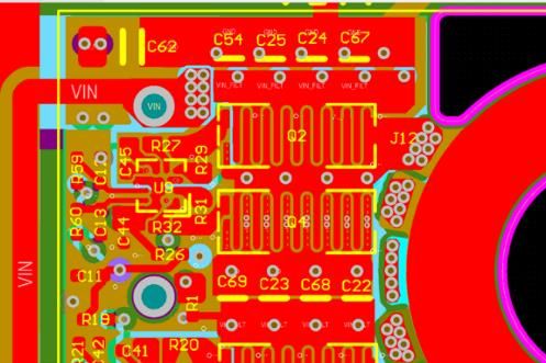
Fig. 1. Fourth generation eGaN FET (bottom view). This series of transistors is rated for 60 A in a
6.05 mm x 2.3 mm footprint.

2.      Design Overview
In keeping with the trend towards reduced input voltage range, a narrow range input was
chosen to allow the use of a 4:1 transformer ratio. The design was restricted to “commercial
off the shelf” (COTS) parts only. The target power loss budget is 15 W which translates into a
full load efficiency target of 97%. The target design specs are given in Fig. 2.

                                      Minimum       Nominal        Maximum
                         Vin [V]      48            52             60
                         Vout [V]     -             12             -
                         Iout [A]     0             -              42
                         Pout [W]     0             -              500
Fig. 2. Target specifications for eGaN eighth-brick converter demo board.

2.1.        E-brick Challenges

The key challenge for the E-brick format stems from the fact that the performance expectations
are similar to those of larger converters. In particular the controls, the gate drives, isolation and
spacing requirements, and PCB manufacturing tolerances are nearly the same for both E- and
Q-bricks. The volume required for this overhead is approximately independent of converter
size; hence this places a greater challenge for smaller converters.

2.2.        Topology Selection

Several topology options were considered for the design. Soft-switched converters were
considered, but require a great deal more design effort than PWM converters, with regulation
being especially challenging. Thus, we elected to stay with a conventional isolated hard-
switched PWM buck converter with integrated planar transformer. The high speed of the eGaN
FETs allow the use of a 300 kHz switching frequency.
On the primary side, a full-bridge (FB) eliminates the need for a dc blocking capacitor and its
attendant loss and volume. Design margin requires the use of 80 V rated transistors. On the
secondary side, full-bridge (FB), current doubler (CD), and center-tapped (CT) synchronous
rectifier (SR) options were considered. The full-bridge has lower transformer conduction loss
and allows the use of lower voltage transistors, ideally with a 30 V rating, but in practice a 40 V
rated part would be selected for margin and to accommodate ringing. Unfortunately, the FB
has a severe semiconductor conduction loss penalty since there are two switches in series for
most of the switching cycle. The CD and CT designs have two switches in parallel, but require
40 V for the ideal case and 60 V devices in practice. Silicon devices pay a large penalty in
RDS(on) with increasing voltage rating, but the penalty is much smaller for the eGaN devices
[13]. The CD appears advantageous at first glance due to greatly reduced transformer
secondary currents. Unfortunately, this comes at the expense of increased magnetizing and
ripple current. These can be mitigated by adding turns to the transformer and inductors, but
then much of the advantage to be lost. Consideration of these factors resulted in the selection
of the CT approach for the secondary side.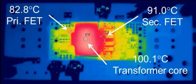
2.3. Benefits of eGaN FETs
eGaN FETs have many benefits over silicon MOSFETs that make them particularly well suited
to E-brick applications. These include reduced gate charge, lower parasitic capacitances and
inductances, lower gate drive voltage, zero reverse recovery, lower specific RDS(on), and faster
switching. It is instructive to compare both eGaN FET and available state-of-the-art silicon
MOSFET candidates for the E-brick application. We wish to compare parts with breakdown
voltages of 80 V (primary) and 60 V (secondary). In practice, primary and secondary total
transistor area should be limited to approximately 120 mm2, e.g. 4 primary transistors with a
total of ~60 mm2 area and two or four secondary devices with a total of ~60 mm2 area. A typical
implementation with silicon MOSFETs would be four 3.3 mm x 3.3 mm DFN primary
transistors and two 5 mm x 6 mm DFN secondary transistors. Fig. 3-4 compare state-of-the-
art commercial devices one would expect to find in a nominal 52 V – 12 V design for an output
synchronous rectifier and input bridge, respectively [6-11]. The footprint area Afootprint is
calculated based on a rectangle that includes the device package envelope and the
manufacturer-recommended printed circuit board pad. Figures 5-6 give figures of merit (FOMs)
for the same devices, which show the expected performance of the EPC eGaN parts to be up
to 14x better than silicon parts, and better than silicon MOSFETs in all cases.
Part Tech. RDS(on) VGS QG QRR [nC] QOSS EOSS Afootprint
[m] [V] [nC] [nC] [nJ] [mm2]
EPC2020 eGaN 1.5 5 16 0 37.6 422 13.9
CSD18540Q5B Si 1.8 10 41 145 49.4 383 30.0
BSC014N06NS Si 1.2 10 89 139 94.1 999 31.7
NTMFS5C604NL Si 0.93 10 120 190 163 1824 31.7
Fig. 3. Parameters for 60 V rated transistors at VDS = 26 V.
Part Tech. RDS(on) VGS QG QRR [nC] QOSS EOSS Afootprint
[m] [V] [nC] [nC] [nJ] [mm2]
EPC2021 eGaN 1.8 5 15 0 68.1 1490 13.9
AON7280 Si 6.8 10 27 162 33.7 575 11.2
BSZ075N08NS5 Si 6.2 10 24 39 32.2 557 12.9
FDMC86430 Si 5.0 10 38 25 45.3 896 11.6
Fig. 4. Parameters for 80 V rated transistors at VDS = 52 V.
Part EgRDS(on) QrrRDS(on) QossRDS(on) EossRDS(on) AfootprintRDS(on)
[nJ*m] [nC*m] [nC*m] [nJ*m] [mm2*m]
EPC2020 120 0 56 633 20.9
CSD18540Q5B 738 (6.2x) 261 89 (1.6x) 689 (1.6x) 62.2 (3.0x)
BSC014N06NS 1068 (8.9x) 167 113 (2.0x) 1199 (2.0x) 41.1 (2.0x)
NTMFS5C604NL 1116 (9.3x) 177 163 (2.7x) 1824 (2.7x) 31.1 (1.5x)
Fig. 5. FOMs for 60 V rated transistors at VDS = 26 V. Relative value of Si MOSFET FOM to eGaN FET
FOM in parentheses. Smaller is better.
Part EgRDS(on) QrrRDS(on) QossRDS(on) EossRDS(on) AfootprintRDS(on)
[nJ*m] [nC*m] [nC*m] [nJ*m] [mm2*m]
EPC2021 135 0 123 2682 25.0
AON7280 1836 (13.6x) 1102 229 (1.9x) 3910 (1.5x) 76.3 (3.0x)
BSZ075N08NS5 1488 (11.0x) 242 200 (1.6x) 3453 (1.3x) 79.8 (3.2x)
FDMC86430 1900 (14.1x) 125 227 (1.8x) 4480 (1.7x) 57.8 (2.3x)
Fig. 6. FOMs for 80 V rated transistors at VDS = 52 V. Relative value of Si MOSFET FOM to eGaN FET
FOM in parentheses. Smaller is better.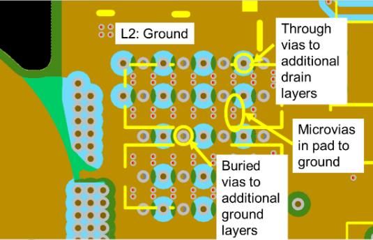
While FOMs such as QGRDS(on) and QOSSRDS(on) are now commonly used, they don’t tell the
whole story. The eighth-brick format has severe constraints. First of all, if one can’t minimize
RDS(on) alone, one cannot achieve the target. One must consider how much transistor area is
needed to achieve the necessary RDS(on), accounted for by the FOM AfootprintRDS(on). The eGaN
parts show a benefit of 1.5x - 3.0x over the silicon MOSFETs for this metric. Secondly, gate
power can be a substantial part of total losses. This is captured by the EgRDS(on) FOM. For the
silicon MOSFETs, the gate power is comparable to or exceeds Eoss by as much as 2x! For an
E-brick design running at 300 kHz, total gate power consumption is < 0.2 W for the eGaN FET
parts, but if enough silicon is used to achieve the same conduction loss, the total gate power
is 1.6 W at a minimum, nearly 11% of the entire loss budget! The gate power of the silicon
devices can be reduced by using a lower gate voltage, but at the expense of greatly increased
conduction loss.
Reverse conduction also differs between eGaN FETs and silicon MOSFETS. eGaN FETs have
an effective reverse diode inherent to the transistor [13], so are suitable for SR applications.
This diode is extremely fast and has no reverse recovery charge (Qrr = 0). Silicon MOSFETs
have high reverse recovery charge (Qrr) that can exceed Qoss (Figures 5-6). This can cause
large increases in switching loss beyond those due to Qoss. Qrr is a highly non-linear function
that depends on operating point and increases strongly as temperature increase. Controlling
reverse recovery loss in silicon is difficult and conflicts with the need to minimize reverse
conduction. The zero Qrr of the eGaN FET is a tremendous advantage. The eGaN FET does
have higher reverse voltage drop than typical of silicon MOSFET body diodes. However, the
absence of Qrr and the high switching speed of the devices means that the reverse conduction
time can be easily minimized.

3.             Detailed E-brick design
3.1.                    Power stage

Fig. 7 shows the basic power stage design, consisting of a primary full-bridge driving a 4:1:1
center-tapped transformer with synchronous rectification. In addition, there is a bias supply, a
controller, and an active snubber. There are several considerations beyond topology, namely
transistor selection, switching frequency, magnetic component selection and design, gate
driver choice, controller approach, current sensing approach, how to deal with transformer
leakage inductance, and layout philosophy and implementation. A rigorous analysis is beyond
the scope of the paper, but a brief explanation is provided below.
             Lf2 330n
     V_IN+
               Cf1                                                                                                                                                          Lf1 470nH
              12*1uF                                                                                                                                                                                   V_OUT+
                                       Q1               Q2
                                         EPC2021         EPC2021                                                                                                          R2              C1
                                  U1               U3
                        p1                  p2                                                                                                                  D4
                                                                              vsa                                                                         vsa             5.2k          100n
                                                          vp+           1T
     V_IN-
                                                                4T            vsct
                                                                                                                                                                            I_OUT_SNS

                                                                                                                                                                                        V_OUT_SNS

                                                          vp-                                                                                                                                       Cf
                                                                        1T
                                                                              vsb                                                   vsb                         D5                                  12*4.7uF

                                                                                                                                            M1              M2
                                       Q3               Q4                           Q5                   Q7
                                        EPC2021 U4       EPC2021                                                               U7                    U8
                                                                                                                        snb1

                                                                                                                                              snb2

                                  U2
                        p2                 p1
                                                                                     EPC2020              EPC2020                                                                                      V_OUT-
                                                                                                                                    Vsnub

                                                                                           Q6                   Q8
                                                                                                                                                                     D1
                                                                                                                                            C2
                                                                                          EPC2020                EPC2020                    470nF
                                                                         U5
                             U10                                   s1                      s2
                                       V_BIAS_PRI
                                                                                                U6
                                                                                                                                     A1
                                                                                                                 Controller                  p1
                             U9                                                                                                      A2
                                       V_BIAS_SEC                                                    V_OUT_SNS                               p2
                                                                                                                                             s1
                                                                                                     I_OUT_SNS                               s2
                                                                                                                                             snb1
                                                                                                                                             snb2

Fig. 7. Simplified schematic of 500 W E-brick converter.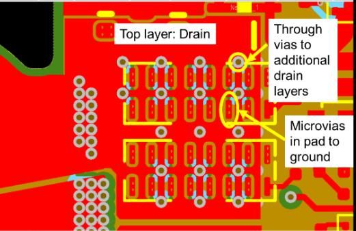
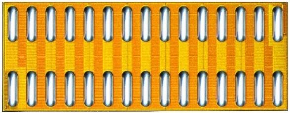
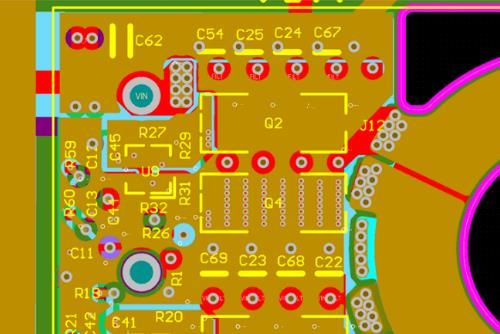
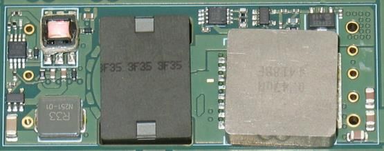
The EPC2021 and EPC2020 eGaN FETs were selected for the primary FB and secondary SR, respectively, based on the eGaN FETs’ superior FOMs. The area of the EPC2020 is such that two parallel FETs can be used for each SR switch in approximately the same area as a single Si MOSFET. Typical E-bricks have switching frequencies of 150 kHz – 200 kHz, but the low switching loss of eGaN FETs enables a switching frequency of 300 kHz to minimize output inductor size and magnetizing current. Two LM5113 half-bridge gate drivers are used on the primary side, with two UCC27611 low side drivers on the secondary. The negligible gate drive power of the eGaN devices means that the smallest gate drive packages can be used (2 mm x 2 mm), saving valuable real estate. The transformer was implemented as 4:1:1 fully interleaved integrated planar transformer. The primary uses one layer per turn, and each secondary uses 4 layers in parallel to form the single turn, resulting in a 12 layer board. The core is a FerroxcubeTM EQ20/R+PLT20 planar core combination in 3F35 material, chosen because it was the largest readily available core that would fit in the E-brick envelope. For the output inductor, the Vishay IHLP6767 series proved suitable. Based on simulation and analysis, a value of 470 nH was chosen. The inductor DCR is used for current sensing. This choice was due to space constraints and the need to minimize any losses, although it forces some compromises on the control approach. Voltage spikes on the secondary side due to parasitic inductance are controlled via a low-loss active snubber [12]. The SR turn-off spike is clamped to Vsnub via D4, D5, and C2. After the spike is clamped, M1 or M2 turns on to allow the charge to flow back to the output through the transformer secondary, simultaneously resetting C2. The converter is controlled by a MicrochipTM dsPIC33FJ16GS502 16-bit microcontroller which includes a high-speed 6-phase PWM with 1.04 ns resolution. Two pairs of phases drive the primary and secondary switches, and the third pair is used to drive the snubber. This resolution, combined with high speed switching of the eGaN FETs and the short propagation delays of the gate drive chips, allows precise control of all switches. This helps to ensure V•s balance on the transformer, minimize reverse conduction time, and control snubber reset timing. The layout is crucial to the proper operation of the circuit. First, to take full advantage of the high switching speed of eGaN FETs, one must minimize power loop inductance. An optimal layout for half-bridges is given in [14]. Although it cannot be exactly applied to the E-brick, the guiding principle still applies, and the high layer count of the PCB allows an excellent approximation. Secondly, due to the lack of a dc blocking cap or accurate current sensing, careful attention must be paid to physical symmetry in order to minimize imbalances on the transformer. The printed circuit board was implemented as a 12 layer board. The ten inner layers are 4 oz. (140 m) copper to handle the high currents, and the outer layers are 2 oz. (70 m) to accommodate the finer pitch of the surface mount components. In addition, the board uses 3 types of vias: through vias, buried vias (layers 2-11), and microvias (layers 1-2 and 11-12). All vias are filled and plated to allow via-in-pad design with reliable soldering. Fig. 8 illustrates the layout used under the SR. Only the top two layers are shown, as the structure is replicated through the remaining layers. The left-hand figure shows the top layer of one of the SR switches using two parallel EPC2020 eGaN FETs. The top layer is one of four layers forming the parallel windings of one of the transformer secondaries, and through vias are used to interconnect these layers. The EPC2020 source pads use microvias in the pad to connect to layer 2, which is a power ground layer that fills the entire secondary side of the board, including a minimum inductance connection to the other SR pair. There are four power ground planes which are all on internal layers, and these are connected to each other using the blind vias as shown on the right-hand side of the figure. Fig. 9 shows the layout of one of the primary half-bridges, with layer 1 (top) on the left and layer 2 on the right. The optimal layout principles are followed more closely here, but are modified because the placement of through vias is limited due to component placement on the bottom side of the board. This is made up for with the use of the microvias, which allow an extremely low impedance connection to layer 2 (power ground). The basic structure is
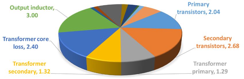
repeated through the board. The entire half-bridge structure is repeated to connect to the other
primary winding terminal.
Finally, the board is intended as a demonstration. This means that low inductance test points
power interconnects, and voltage test points. As a result, the board is extended beyond the
normal E-brick boundary. However, all converter components are included in the boundary,
including holes for connection pins, in order to have as fair a comparison as possible. Where
possible, the board includes a moat to thermally separate the outer copper of the demo board
from the converter area. Fig. 10 shows photographs of the converter, and the entire demo
board is shown in Fig. 13.

Fig. 8. Detailed view of the first two layers for the upper right eGaN FET part comprising one of the two
SR switches.

Fig. 9. Detailed view of the first two layers for the upper left eGaN FET pair comprising one of the two
primary half-bridges.

Fig. 10. Photograph of E-brick demo board: top view (left), bottom view (right).

3.2.        Loss Analysis

Figure 11 shows a predicted loss breakdown based on a combination of analysis and
simulation. The simulation models include estimated stray inductance and capacitance, as well
as losses in the magnetics. They do not include losses due to vias, solder joints, connection
pins, or capacitor ESRs, although an allowance is provided for these. The total loss breakdown
also includes controls, bias supply, miscellaneous support circuitry While all simulations should
be viewed cautiously, one of the key sources of simulation error, poor reverse recovery
modeling, has been eliminated, hence the results are likely to more closely reflect reality.
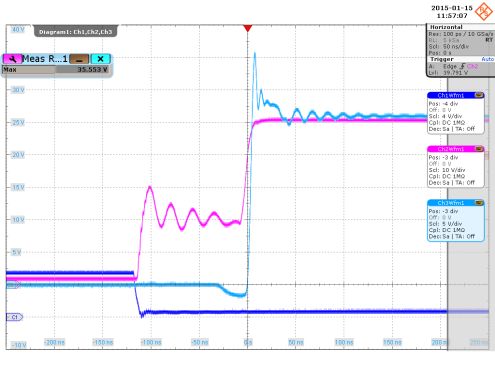
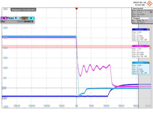
4. Results Room temperature efficiency and power loss versus load current are shown in Fig. 12. For the regulated case, peak efficiency is 96.7 % with VIN = 52 up to IOUT = 42 A. Fig. 13 shows an IR thermal image of the converter with VIN = 52 V at full load (42 A) with approximately 400 LFM (2 m/s) airflow at thermal steady state. Even in this case, it still has an efficiency > 96.4%. The transformer core is the hottest component at only 101C. The converter loses regulation due to a duty cycle clamp below 49 V, but the droop is low (Fig. 14)., and indicates an unregulated output resistance of 9.8 m. Fig. 14 also shows the main converter waveform for nominal full- load operation, and Fig. 15 gives a close-up view of the switching transitions. Fig. 11. Predicted loss breakdown showing main losses. Total predicted loss is 16.6 W at 100C. Fig. 12. Room temperature efficiency and power loss versus load current For VIN > 49 V, 500 W output occurs at 41.7 A. Below VIN = 49 V, duty cycle is clamped and there is a small output voltage droop, shown in Fig. 14. Fig. 13. Thermal image of E-brick demo board in thermal steady state. VIN = 52 V, IOUT = 42 A with ~400 LFM (2 m/s) airflow. 5. Conclusion The analysis and results show that eGaN FETs suitable for brick-type dc-dc converters have superior electrical performance compared to silicon MOSFETs of similar size, for both conduction loss and switching loss. It is further shown that the benefit can be realized in practice via the development of a 300 kHz E-brick demonstration converter using eGaN FETs for all main power switches. This converter can provide a fully regulated 12 V output at over 42 A, for an output power > 500 W with peak efficiency of 96.7% at 42A at room temperature.
It maintains high efficiency running hot. At thermal steady state with full load (42 A) efficiency is > 96.4% at 400 LFM (2 m/s) of 25C airflow. This converter shows that a 500 W eighth-brick converter is made not only possible, but practical, using eGaN FET technology. Fig. 14. Left: Output voltage versus load current with ~400 LFM (2 m/s) airflow. The VIN = 48 V case is unregulated. Right: Main converter waveforms with VIN = 52 V, IOUT = 42 A. Fig. 15. Detailed switching waveforms for VIN = 52 V, IOUT = 42 A. Turn-on (left) and turn-off (right). 6. References [1] “Second Generation Eighth Brick DC/DC Converter with Digital Connections,” Distributed- Power Open Standards Alliance (DOSA), www.dosapower.com, June 2010. [2] “QBVE078A0S10R4 Barracuda Series DC-DC Converter Power Module Datasheet,” GE Industrial Solutions Embedded Power, General Electric Company, January 2014. [3] “Delphi E48SP12020 Power Module Datasheet,” Delta Electronics, Inc., August 2011. [4] “EBVE031A0S9R6 Barracuda Series DC-DC Converter Power Module Datasheet,” GE Industrial Solutions Embedded Power, General Electric Company, December 2013. [5] “NEB-D Fully Regulated Advanced Bus Converter Datasheet,” CUI Inc, March 2014. [6] “EPC2021 Datasheet,” Efficient Power Conversion Corp., July 2014. [7] “EPC2024 Datasheet,” Efficient Power Conversion Corp., July 2014. [8] “AON6278 Datasheet,” Alpha & Omega Semiconductor, March 2014. [9] “AON6230 Datasheet,” Alpha & Omega Semiconductor, February 2013. [10] “BSZ075N08NS5 Datasheet,” Infineon Technologies AG, May 2014. [11] “BSZ028N04LS Datasheet,” Infineon Technologies AG, September 2013. [12] D. Dalal and F.-S. Tsai, “A 48V, 1.5kW, Front-End Zero-Voltage-Switched, PWM Converter with Lossless Active Snubbers for Output Rectifiers,” 1993 Applied Power Electronics Conference and Exposition (APEC) Conference Proceedings, pp. 722-728. [13] A. Lidow, J. Strydom, M. de Rooij, D. Reusch, “GaN Transistors for Efficient Power Conversion,” Second Edition, Wiley, 2014. [14] D. Reusch and J. Strydom, “Understanding the Effect of PCB Layout on Circuit Performance in a High Frequency Gallium Nitride Based Point of Load Converter,” Applied Power Electronics Conference and Exposition (APEC), pp.649-655, 2013.
You can also read