Quantum spin Hall effect in two-dimensional transition-metal chalcogenides
←
→
Page content transcription
If your browser does not render page correctly, please read the page content below
Quantum spin Hall effect in two-dimensional transition-metal chalcogenides

                                                             Xing Wang,1, 2 Wenhui Wan,1 Yanfeng Ge,1 Kai-Cheng Zhang,3 and Yong Liu1, ∗
                                                                 1
                                                                     State Key Laboratory of Metastable Materials Science and Technology &
                                                                  Key Laboratory for Microstructural Material Physics of Hebei Province,
                                                                         School of Science, Yanshan University, Qinhuangdao 066004, China
arXiv:2109.01209v3 [cond-mat.mtrl-sci] 30 Sep 2021

                                                                     2
                                                                         College of Science, Hebei North University, Zhangjiakou 07500, China
                                                                                        3
                                                                                            College of Mathematics and Physics,
                                                                                      Bohai University, Jinzhou 121013, China
                                                                                                  (Dated: October 1, 2021)

                                                                                                        Abstract
                                                       Based on first-principles calculations, we have found a family of two-dimensional (2D) transition-metal
                                                     (TM) chalcogenides MX5 (M = Zr, Hf and X = S, Se and Te) can host quantum spin Hall (QSH) effect.
                                                     The molecular dynamics (MD) simulation indicate that they are all thermal-dynamically stable at room
                                                     temperature, the largest band gap is 0.19 eV. We have investigated MX5 ’s electronic properties and found
                                                     their properties are very similar. The single-layer ZrX5 are all gapless semimetals without consideration of
                                                     spin-orbit coupling (SOC). The consideration of SOC will result in insulating phases with band gaps of 0.05
                                                     eV (direct), 0.18 eV (direct) and 0.13 eV (indirect) for ZrS5 , ZrSe5 to ZrTe5 , respectively. The evolution
                                                     of Wannier charge centers (WCC) and edge states confirm they are all QSH insulators. The mechanisms
                                                     for QSH effect in ZrX5 originate from the special nonsymmorphic space group features. In addition, the
                                                     QSH state of ZrS5 survives at a large range of strain as long as the interchain coupling is not strong enough
                                                     to reverse the band ordering. The single-layer ZrS5 will occur a topological insulator (TI)-to-semimetal
                                                     (metal) or metal-to-semimetal transition under certain strain. Monolayer MX5 expand the TI materials
                                                     based on TM chalcogenides and may open up a new way to fabricate novel low power spintronic devices at
                                                     room temperature.

                                                     PACS numbers: 61.82.Ms, 73.20.At, 71.20.-b, 73.43.-f

                                                                                                            1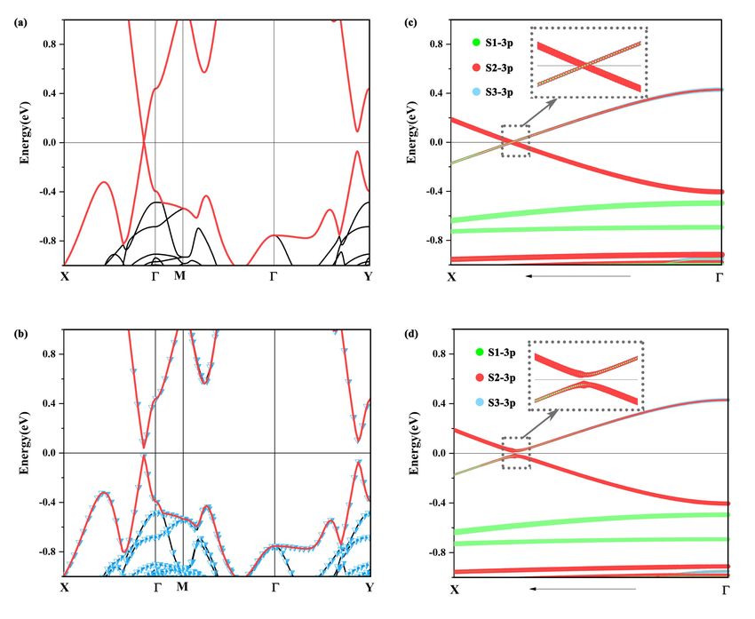
I. INTRODUCTION

   Under the influence of graphene stripping from graphite, more and more two-dimensional (2D)
materials are obtained by stripping block layered materials1–3 . These successfully prepared 2D
materials have aroused great interest of scientists because of their excellent properties and great
application prospects4–8 . Among them, 2D topological insulators (TIs) are of great significance
to the study of condensed matter and materials science because of their fresh topological phases.
The 2D TIs, also called quantum spin Hall (QSH) insulators, have fully spin-polarized gapless
edge states into an insulating bulk. The QSH effect was first proposed by Kane and Mele in
graphene9–11 , but its small energy gap of 10−3 meV makes it hard to be observed experimentally.
The HgTe/CdTe quantum wells12,13 have been first realized in experiment, but it needs precisely
controlled molecular beam epitaxy (MBE) growth at ultralow temperature. In the passed years,
extensive efforts have been devoted to search new QSH insulators, a growing number of com-
pounds have been predicted to be 2D TIs14–23 . Due to the lack of suitable materials that are easy
to prepare, stable in structure and large in band gap, the research of 2D TIs has been seriously
hindered. Therefore search larger gap 2D TIs from the common used materials is indispensable
for their ultimate realization.

   At present, intensive research on transition metal (TM) based QSH insulators has greatly en-
riched the family of QSH insulators24–26 , showing band inversion is caused by strong electron
interaction rather than spin-orbit coupling (SOC). TM atom-based TIs are rare and only several
examples are reported. Among them, the MTe5 (M = Zr, Hf) have attracted broad attention because
of their topogical properties27–35 . Three-dimensional (3D) MTe5 is a layered crystal with weak in-
terlayer coupling, which is comparable to graphite. The MTe5 monolayer may be obtained via the
mechanical exfoliation from the 3D bulk phase as like producing graphene from graphite36,37 . The
2D crystals are predicted to be QSH insulators with the band gap about 0.1 eV27 . In addition, TM
halide MX (M = Zr, Hf; X = Cl, Br and I) monolayer has to be found the 2D QSH insulators19 .
Material design or atomic substitution may lead to more and better 2D TIs. Here we study TM
chalcogenides MX5 (M = Zr, Hf; X = S, Se and Te) and different TM chalcogenides may have
different topological properties. What’s more, we try to use the strain to increase the band gap of
TM chalcogenides.

   In this work, we have investigated the structural stability and electronic structure of single-layer
MX5 by using first-principles calculations. The single-layer ZrX5 and HfX5 have very similar

                                                 2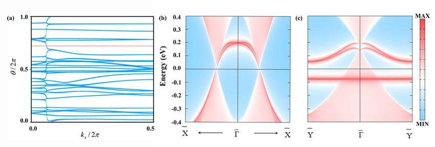
properties, they are all QSH insulators with the largest band gap of 0.19 eV. Then we take ZrX5
as an example, they are all gapless semimetals without consideration of SOC. The consideration
of SOC will result in QSH insulators with band gaps of 0.05 eV (direct), 0.18 eV (direct) and
0.13 eV (indirect) for ZrS5 , ZrSe5 to ZrTe5 , respectively. The topological invariant Z2 =1 and edge
states confirm the nontrivial topological nature of these materials. The mechanism of QSH effect
in ZrX5 originates from the special nonsymmorphic space group features. In addition, the QSH
state of ZrS5 survives over a very large strain range until the interchain coupling is strong enough
to reverse the band ordering.
II. COMPUTATIONAL DETAILS
The Vienna ab initio Simulation Package (VASP)38,39 is used to study the structural and elec-
tronic properties of MX5 . The exchange correlation interaction is treated within the generalized
gradient approximation (GGA)40 of Perdew, Burke and Ernzerhof (PBE)41 . The Brillouin zone
(BZ) is integrated with 13 × 4 × 1 Γ-centered Monkhorst-Pack grid42 , the plane-wave cutoff en-
ergy is set to 500 eV with the energy precision of 10−5 eV. A more than 20 Å vacuum slab along
z-direction is set to avoid interactions between neighboring slabs. The atoms in the unit cell are
relaxed until the force on each atom is less than 0.01 eV/Å. Since PBE methods often underesti-
mate the band gap, the hybrid functional HSE0643 is used to check the results and the band gaps
are very similar. Further, the local orbital basis suite towards electronic-structure reconstruction
(LOBSTER)44–46 has been used to extract the chemical-bonding information for ZrX5 . The tight
binding matrix elements are calculated by projecting the Bloch states onto maximally localized
Wannier functions (MLWFs)47,48 using the VASPWANNIER90 interface. The MLWFs are de-
rived from M’s d and X’s p orbitals by using the Wannier90 code47,48 . The WannierTools49 is used
to analyse topological properties after successful constructions of the MLWFs.
III. RESULTS AND DISCUSSION
13
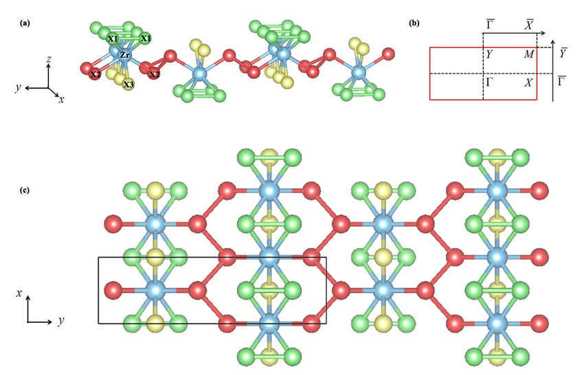
The MX5 monolayer has the orthorhombic structure with Pmmn (D2h ) nonsymmorphic space
group shown in Fig. 1 (a). The trigonal prismatic chains X1-X3-X1 oriented along the x axis,
and these prismatic chains are linked via parallel zigzag chains of X2 atoms along the y axis to
form a 2D sheet of MX5 in the x-y plane. We choose the origin of the coordinate system located
3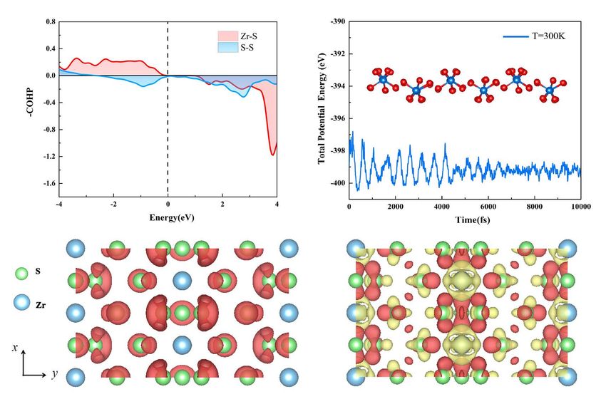
FIG. 1. (Color online) The side view (a) and top view (c) of relaxed single-layer MX5 . Blue balls are M
atoms and the other color balls are X atoms. The primitive cell is shown in black rectangle. (b) 2D and
projected edge first BZ with high symmetry points (blue dots).

on Zr site, so the inversion center is located at (0.25, 0.25). The two X1 (or X2) atoms in the
same chain have mirror symmetry, while the two X3 (or X2) atoms in the adjacent prism (or same
zigzag) chain have inversion symmetry. The optimized lattice constants of single-layer MX5 are
summarized in Table I. The relaxed lattice constants (a= 4.047 Å, b= 13.860 Å) of ZrTe5 are nearly
same to the reference value ( a= 4.036 Å, b= 13.843 Å)27 . The lattice constants have increase trend
with increasing atomic radius of X atom in ZrX5 and HfX5 monolayer. While fixed chalcogenide
atoms, the atomic radius of Zr and Hf are affected by lanthanide contraction effect50 , so the lattice
constants show opposite variation trends, similar to the ZrCl and HfCl19 . The single-layer ZrX5
and HfX5 have very similar properties, hereafter, we take ZrX5 as an example.
   First, we use the crystal orbital Hamilton population (COHP) method to extract the chemical-
bonding information, shown in Table II. The bond lengths increase from ZrS5 , ZrSe5 to ZrTe5 ,
and it makes sense because the atomic radius increases from S, Se to Te. The Fermi levels in
Fig. 2 (a) and supplemental material (SM) Fig. S1 lie in the COHP curve between the bonding
and antibonding regions. Fousing on the plots below the Fermi level, the majority of the bonding
interactions resides the atoms Zr-X, the majority of the antibonding interactions reside the atoms
X-X. But there are not many populated antibonding states, which doesn’t lead to an enormous in-

                                                  4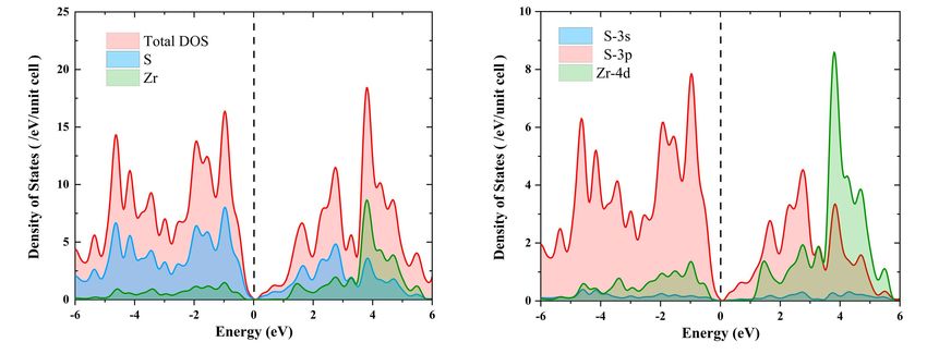
ternal stress, so the materials are relatively stable. The integrated COHP (ICOHP) values increase
from ZrS5 , ZrSe5 to ZrTe5 , which indicates the material stability decreases in turn. In addition, the
binding energy of -2.305, -1.985 and -1.613 eV/atom indicates the materials are all stable. More-
over, we examine thermal stability of ZrX5 by performing ab initio molecular dynamics (MD)
simulation. After heating at 300 K for 10ps with a time step of 2fs, it is found that the average of
the total potential energy remains constant throughout the simulation time, see Fig. 2 (b) and Fig.
S2. These materials do not undergo structural reconstruction or damage. These results indicate
clearly the materials remain thermal dynamically stable at room temperature.
   Then the electron localization function (ELF)51 are used to describe and visualize chemical
bonds in ZrX5 monolayer. The result for single-layer ZrS5 is illustrated in Fig. 2 (c) for the ELF =
0.88 isosurface. The greater value of S-S bonding suggests anti-bonding character, while the Zr-S
bonding indicates the highly ionic nature. Charge transfer of Zr-S bonding is studied by difference
charge density diagram, as shown in Fig. 2 (d). The charge accumulation (loss) is represented by
red (yellow) region, the major charge transfer is from Zr atom to S atom, which is consistent with
ionic bonding. The ZrSe5 and ZrTe5 have similar characters, presented in Fig. S3 and S4.

TABLE I. The lattice constants a, b, global band gap Eg , band gap at Γ point EΓ and Z2 invariant of single-
layer MX5 .

                                Material a(Å)   b(Å) Eg (eV) EΓ (eV) Z2

                                 ZrS5    3.529 11.679 0.050      0.835   1
                                 ZrSe5 3.731 12.487 0.181        0.509   1
                                 ZrTe5 4.047 13.860 0.129        0.400   1

                                 HfS5    3.499 11.637 0.049      0.757   1
                                 HfSe5 3.703 12.457 0.187        0.474   1
                                 HfTe5 4.020 13.853 0.106        0.383   1

   To further understand of their electronic properties, we have calculated the total density of states
(DOS) and projected density of states (PDOS) with consideration of SOC for ZrX5 , shown in Fig.
3 and Fig. S5. The small band gaps near the Fermi levels indicate they are all semiconductors, so
we take the ZrS5 as an example. The PDOS clearly show that around Fermi level the S covalently
bonded p states are dominant. The d orbitals of Zr are mainly located at the level of 4eV above
the Fermi level, leading to the nearly ionic states. These results are consistent with the previous

                                                   5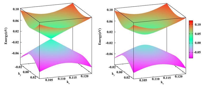
TABLE II. The bond lengths and ICOHP values of ZrTe5 , ZrSe5 and ZrS5 , respectively.

               2D       dZr−X1 ICOHPZr−X1 dZr−X2 ICOHPZr−X2 dZr−X3 ICOHPZr−X3
            Materials    (Å)    (eV/bond)       (Å)     (eV/bond)      (Å)     (eV/bond)

              ZrS5       2.56       -3.03       2.67         -2.40       2.58       -2.74
              ZrSe5      2.74       -2.54       2.78         -2.35       2.75       -2.54
              ZrTe5      2.97       -2.04       2.99         -2.08       3.01       -2.21

   (
   a)                                                   (
                                                        b)

   (
   c)                                                   (
                                                        d)

FIG. 2. (Color online) The crystal orbital Hamilton population (COHP) curves, molecular dynamics (MD)
simulation, electron localization function (ELF) and difference charge density of single-layer ZrS5 . (a)
The COHP curves. The Fermi levels are marked by the vertical dashed lines. (b) Snapshots of atomic
configurations at the end of MD simulation and total potential energy fluctuations observed at 300K. (c)
Structure plot of ELF. Isosurface corresponding to ELF value of 0.88. (d) Difference charge density. The
red (yellow) isosurface plots correspond to the charge density accumulation (depletion).

                                                   6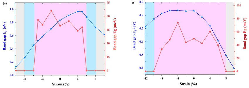
discussion.
  (
  a)                                                    (
                                                        b)

FIG. 3. (Color online) The total density of states (DOS) (a) and projected density of states (PDOS) (b) with
consideration of SOC for single-layer ZrS5 . The Fermi levels are set to zero and marked by vertical dashed
lines.

   The calculated band structures for a single-layer ZrX5 are displayed in Fig. 4 and Fig. S6.
They are all gapless semimetals without consideration of SOC, the conduction band minimum
(CBM) and valence band maximum (VBM) touch each other at the Γ-X direction. In Fig. 5 (a),
we plot the ZrS5 ’s band dispersion around this crossing point, which demonstrates that the Dirac
point is isolated and has linear dispersion. The consideration of SOC will result in insulator phase
and the large band gaps at Γ point decrease from ZrS5 , ZrSe5 to ZrTe5 , shown in Table I. The
global band gaps of 0.05 eV (direct), 0.18 eV (direct) and 0.13 eV (indirect) for ZrS5 , ZrSe5 to
ZrTe5 , respectively. The ZrS5 and ZrSe5 are more suitable than ZrTe5 as materials for making
photoelectric devices. We can clearly see a small gap will be opened at the original Dirac point
and the low-energy electrons become 2D massive Dirac fermions in Fig. 5 (b). The evolution
lines of Wannier centers in Fig. 6 (a) and Fig. S7 show they are all nontrivial QSH insulators with
Z2 =1 and the important character of helical edge states also appear, as shown in Fig. 6 (b, c) and
Fig. S8. The nontrivial Z2 invariants guarantee that the edge bands always cut the Fermi level an
odd number of times. The helical edge states form bands crossing linearly at the Γ point for the
x axis edge in the bulk gap. Each edge has a single pair of helical edge states for these systems.
The two counter-propagating edge states display opposite spin-polarizations is the typical feature
of a QSH phase. Helical edge states are very important in electronics and spintronics because of
their topological robustness to scattering. As an important characterization related to application,

                                                   7
FIG. 4. (Color online) The band structures of single-layer ZrS5 for (a, c) without and (b, d) with SOC case.
The blue triangles indicate the band structures diagrams calculated by Wannier90. The enlarged orbitals-
resolved band structures are shown in insets. The green, red and blue circles represent the weights of the
S1-3p, S2-3p and S3-3p orbitals character, respectively. The Fermi levels are set to be zero.
the Fermi velocity of helical edge states are about 1.0 × 10⁴ m/s, 2.3 × 10⁵ m/s and 2.0 × 10⁵
m/s for ZrS5 , ZrSe5 to ZrTe5 , respectively. The values are a little smaller than these for stanene
(4.4 × 10⁵ m/s), fluorinated stanene (6.8 × 10⁵ m/s), and HgTe quantum well (5.5 × 10⁵ m/s)15 .
It can be expected that the ZrSe5 and ZrTe5 are more suitable than ZrS5 as candidate materials for
high-speed devices. For the edge along the y axis, the symmetric edge structure leads to two Dirac
cones located at opposite Y points. The topological nature of monolayer ZrX5 is further confirmed
by the nontrivial metallic edge states.
8(
a) (
b)
FIG. 5. (Color online) The 3D band structures of single-layer ZrS5 (a) without and (b) with SOC, respec-
tively. The Fermi levels are set to zero.
FIG. 6. (Color online) The evolution of Wannier charge centers (WCC) and edge states of single-layer ZrS5 .
(a) The evolution of WCC along kx . The evolution blue lines cross the arbitrary reference red line one time
yielding Z2 =1. The edge state for (b) x edge and (c) y edge.
To get a physical understanding of the topological nature, we present the orbitals-resolved
band structures in Fig. 4 (c, d) and SM Fig. S6, it can be seen the bands around the Fermi level
are mainly derived from X1-p and X2-p orbitals for ZrX5 , so they have the same band inversion
mechanism as ZrTe5 27 . The mechanism for QSH effect in ZrX5 originates from the special non-
symmorphic space group features, X1 state has odd parity lead to the total parity of the occupied
states is negative, which leads to the QSH state.
9Se
Se
Se
TI
TI
Me
Me
Me
mi
mi
mi
t
t
t
a
a
a
me
me
me
l
l
l
t
t
t
a
a
a
l
l
l
FIG. 7. (Color online)The variation of band gap as a function of uniaxial strain along the (a) [100] and (b)
[010] direction of single-layer ZrS5 . Eg and EΓ represent the globe band gap and direct band gap at the Γ
point, respectively. The nontrivial Z2 topology survives as long as the globe band gap remains positive.
Further more, we study electronic properties of single-layer ZrS5 under different strain to ex-
plore the possible phase transition. For the uniaxial strain along the [100] and [010] directions, the
variation of band gap as a function of strain is presented Fig. 8. Strain has little effect on the global
band gap Eg , but greatly affects band gap at the Γ point band gap EΓ . For the [100] uniaxial strain,
the EΓ increases first then decreases from -10 % to 10% and reaches a maximum value of 0.97 eV
at 4% tensile strain. The Eg varies with strain and reaches a maximum value of 66.0 meV at 2%
compressive strain. When the compressive (or tensile) strain is more than 6%, the band structure
produces a TI-to-metal transition. When the compressive (or tensile) strain is more than 8%, the
band structure produces a metal-to-semimetal transition.
For the [010] uniaxial strain, the EΓ also increases first then decreases from -12% to 10%,
reaches a maximum value of 0.84 eV at 4% compressive strain. However, the Eg value changes
very little with strain, reaches a maximum value of 74.2 meV at 4% compressive strain. When the
compressive strain is more than 10%, the band structure produces a TI-to-semimetal transition.
When the tensile strain is more than 8%, the band structure produces a TI-to-metal transition. In
a word, the nontrivial topological phases survive over a wide strain from -6% to 6% along [100]
direction or -10% to 8% along [010] direction, as long as the interchain coupling is not strong
enough to reverse the band ordering near the Fermi energy, the QSH state should be stable, such
robust topology gainst lattice deformation may make it easier for experimental realization and
characterization on different substrate.
10Finally, we have analyzed the electronic and topological properties for HfX5 monolayer and
draw the same conclusions as ZrX5 . HfX5 mnolayer materials also possess QSH states with Z2 =
1, remain thermal dynamically stable at room temperature, and their band structures and band-gap
sizes are very similar to ZrX5 ’s, see Table II, Fig. S9 and Fig. S10.
IV. CONCLUSION
In summary, we have found a family of 2D MX5 can host QSH effect. The MD simulation
indicates they are all thermal-dynamically stable at room temperature, they are all QSH insulators
with the largest band gap is 0.19 eV. The single-layer ZrX5 and HfX5 have very similar properties.
The evolution of WCC and edge states verifies the nontrivial topological nature of these materials.
The Dirac points of these materials have high velocities, so they can be used as candidates for
high-speed electronic devices materials. The mechanism for QSH effect in ZrX5 originates from
the special nonsymmorphic space group features, X1 state has odd parity lead to the total parity of
the occupied states is negative, which leads to the QSH state. In addition, the QSH state of ZrS5
survives at a large range of strain as long as the interchain coupling is not strong enough to re-
verse the band ordering. The band structure of single-layer ZrS5 can produce transition among TI,
semimetal and metal under certain strain. These simple monolayer ZrX5 without chemical deco-
ration, which are very favorable for the future experimental implementation via simple exfoliation
from its 3D system, making them highly adaptable to various environments. These significant
results may promote the further study of QSH insulators based on TM chalcogenide.
ACKNOWLEDGMENTS
This work was supported by National Natural Science Foundation of China (No. 11904312 and
11904313), the Project of Department of Education of Hebei Province, China(No. BJ2020015),
and the Natural Science Foundation of Hebei Province (No. A2019203507 and A2020203027).
K.C. Zhang acknowledges the fund support from LiaoNing Revitalization Talents Program (No.
XLYC2007120). The authors thank the High Performance Computing Center of Yanshan Univer-
11sity.
∗ yongliu@ysu.edu.cn or ycliu@ysu.edu.cn
1 J. Coleman, M. Lotya, A. Gallagher, S. Bergin, and P. King, Science 331, 568 (2011).
2 K. S. Novoselov, D. Jiang, F. Schedin, T. Booth, V. V. Khotkevich, S. V. Morozov, and A. K. Geim, Proc.
Natl. Acad. Sci. 102, 10451 (2005).
3 Q. L. Bao and K. Loh, ACS Nano 6, 3677 (2012).
4 N. Staley, J. Wu, P. Eklund, Y. Liu, L. Li, and Z. Xu, Phys. Rev. B 80, 184505 (2009).
5 G. C. Andres, N. Agralt, and R. B. Gabino, App. Phys. Lett. 96, 213116 (2010).
6 C. Dean, A. Young, I. Meric, C. Lee, L. Wang, S. Sorgenfrei, and K. Watanabe, Nat. Nanotechnol. 5,
722 (2010).
7 C. G. Andres, W. Magdalena, N. Tombros, and R. B. Gabino, Small 7, 2491 (2011).
8 C. G. Andres, P. Menno, A. Albert, S. Gary, and Z. Herre, Nano Res. 5, 550 (2012).
9 C. L. Kane and E. J. Mele, Phys. Rev. Lett. 95, 226801 (2005).
10 C. L. Kane and E. J. Mele, Phys. Rev. Lett. 95, 146802 (2005).
11 Y. G. Yao, F. Ye, X. L. Qi, S. C. Zhang, and Z. Fang, Phys. Rev. B 75, 041401 (2007).
12 B. A. Bernevig, T. L. Hughes, and S. C. Zhang, Science 314, 1757 (2006).
13 M. König and S. Wiedmann and C. Brüne, Science 318, 766 (2007).
14 Y. Xia, D. Qian, D. Hsieh, L. Wray, and A. Pal, Nat. Phys. 5, 398 (2015).
15 Y. Xu, B. Yan, H. J. Zhang, J.Wang, X. Gang, P. Tang,W. Duan, and S. C. Zhang, Phys. Rev. Lett. 111,
136804 (2013).
16 S. Chen, J. W. Liu, Y. Xu, J. Wu, B. L. Gu, and W. H. Duan, Phys. Rev. B 89, 115429 (2014).
17 Y. D. Ma, L. Z. Kou, Y. Dai, H. Thomas, and X. Li, Phys. Rev. B 92, 085427 (2015).
18 Y. D. Ma, L. Z. Kou, X. Li, Y. Dai, and H. Thomas, Phys. Rev. B 93, 035442 (2015).
19 L. J. Zhou, L. Z. Kou, Y. Sun, C. Felser, and F. M. Hu, Nano Lett. 15, 7867 (2015).
20 Z. Liu, C. X. Liu, Y. S. Wu, W. H. Duan, F. Liu, and J. Wu, Phys. Rev. Lett. 107, 136805 (2011).
21 H. M.Weng, R. Ahmad, Y. Y. Liang, Z. D. Song, M. Khazaei, S. J. Yunoki, F. Zhong, and X. Dai, Phys.
Rev. B 92, 075436 (2015).
22 S. M. Nie, Z. Song, H. Weng, and Z. Fang, Phys. Rev. B 91, 235434 (2015).
23 W. Luo and H. J. Xiang, Nano Lett. 15, 3230 (2015).
1224 A. Go, W. K. William, G. S. Jeon, K. Park, and Y. Kim, Phys. Rev. Lett. 109, 066401 (2012).
25 J. Werner and F. Assaad, Phys. Rev. B 88, 035113 (2013).
26 H. M. Weng, J. Z. Zhao, Z. J. Wang, Z. Fang, and X. Dai, Phys. Rev. Lett. 112, 016403 (2014).
27 H. M. Weng, X. Dai, and F. Zhong, Phys. Rev. X 4, 011002 (2014).
28 R. Wu, J. Z. Ma, and L. X. Zhao, Phys. Rev. X 6, 021017 (2016).
29 Q. Li and D. E. Kharzeev, Nature Phys. 12, 550 (2016).
30 R. Y. Chen and S. J. Zhang, Phys. Rev. Lett. 115, 176404 (2015).
31 X. B. Li and W. K. Huang, Phys. Rev. Lett. 116, 176803 (2016).
32 G. Manzoni and L. Gragnaniello, Phys. Rev. Lett. 117, 237601 (2016).
33 Y. Z. Liu, H. C. Wang, H. P. Zhu, Y. A. Li, and J. Wang, Npj Quan. Mat. 5, 88 (2020).
34 Z. J. Fan, Q. F. Liang, Y. B. Chen, S. H. Yao, and J. Zhou, Sci. Rep. 7, 45667 (2017).
35 P. Shahi, J. D. Singh, P. J. Sun, X. L. Zhao, and F. G. Chen, Phys. Rev. X 8, 021055 (2016).
36 K. Novoselov, Nat. Mater. 6, 720 (2007).
37 M. Dzmitry and A. Kuzmich, Science 306, 663 (2004).
38 G. Kresse and J. Furthmuller, Phys. Rev. B 54, 11169 (1996).
39 G. Kresse and J. Furthmuller, Comput. Mater. Sci. 6, 15 (1996).
40 J. P. Perdew and J. A. Chevary, Phys. Rev. B 46, 6671 (1992).
41 J. P. Perdew, K. Burke, and M. Ernzerhof, Phys. Rev. Lett. 78, 3865 (1996).
42 H. J. Monkhorst and J. D. Pack, Phys. Rev. B 13, 5188 (1976).
43 J. Heyd, G. E. Scuseria, and M. Ernzerhof, J. Chem. Phys. 118, 8207 (2006).
44 R. Dronskowski and P. E. Bloechl, J. Phys. Cherm. 97, 8617 (1993).
45 V. L. Deringer, A. L. Tchougreff, and R. Dronskowski, J. Phys. Chem. A 115, 5461 (2011).
46 S. Maintz, V. L. Deringer, A. L. Tchougreff, and R. Dronskowski, J. Comput. Chem. 37, 1030 (2016).
47 N. Marzari and D. Vanderbilt, Phys. Rev. B 56, 12847 (1997).
48 S. Ivo, M. Nicola, and V. David, Phys. Rev. B 65, 035109 (2001).
49 Q. Wu, S. Zhang, and H. F. Song, Comput. Phys. Commun. 224, 405 (2018).
50 C. E. Housecroft and A. G. Sharpe, Inorganic Chemistry, 4th ed., Lanthanide Contraction, Pearson:
New York, 2008.
51 A. Savin, R. Nesper, S. Wengert, and T. F. Fassler, Angew. Chem. Int. Ed. Engl. 36, 1808 (1997).
13You can also read