The Semiconductor Supply Chain: Assessing National Competitiveness - CSET Issue Brief - Center for ...
←
→
Page content transcription
If your browser does not render page correctly, please read the page content below
January 2021

The Semiconductor
Supply Chain:
Assessing National
Competitiveness
CSET Issue Brief

                   AUTHOR
                   Saif M. Khan
                   Alexander Mann
                   Dahlia Peterson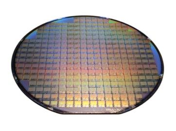
Table of Contents

Executive Summary............................................................................................... 3
Introduction and Overview .................................................................................. 5
Research and Development ............................................................................... 12
Production............................................................................................................ 14
    Design ........................................................................................................................ 15
    Fabrication ................................................................................................................. 19
    Assembly, Testing, and Packaging .......................................................................... 23
Semiconductor Manufacturing Equipment ....................................................... 25
    Wafer Manufacturing, Wafer Marking, and Handling ......................................... 26
    Ion Implanters ............................................................................................................ 28
    Lithography ................................................................................................................ 30
    Deposition .................................................................................................................. 35
    Etch and Clean .......................................................................................................... 39
    Chemical Mechanical Planarization ....................................................................... 42
    Process Control.......................................................................................................... 42
    Assembly and Packaging ......................................................................................... 45
    Testing ........................................................................................................................ 47
Electronic Design Automation and Core IP ...................................................... 49
Materials ............................................................................................................. 51
    Raw Materials ........................................................................................................... 52
    Fab Materials ............................................................................................................ 55
    Packaging Materials ................................................................................................. 61
Conclusion ........................................................................................................... 62
Appendix A: Value Add of Supply Chain Segments ....................................... 63
Appendix B: Glossary ........................................................................................ 65
Acknowledgments .............................................................................................. 68
Endnotes .............................................................................................................. 69

                                                Center for Security and Emerging Technology | 2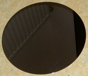
Executive Summary

Advanced computer chips drive economic and scientific advancement as well
as military capabilities. Complex supply chains produce these chips, and the
global distribution of these chains and associated capabilities across nations
have major implications for future technological competition and international
security. However, supply chain complexity and opaqueness make it difficult
to formulate policy. Avoiding unpredicted harms requires detailed
understanding of the complete supply chain and national competitiveness
across each element of that chain.

To help policymakers understand global semiconductor supply chains, we
have broken down these supply chains into their component elements and
identified the features most relevant to policymakers because they either offer
potential targets for technology controls or constrain the policy options
available. A companion CSET issue brief titled “U.S. Semiconductor Exports
to China: Current Policies and Trends” provides an overview of how export
controls are currently applied to semiconductor supply chains.1 Companion
CSET policy briefs titled “Securing Semiconductor Supply Chains”2 and
“China’s Progress in Semiconductor Manufacturing Equipment”3 offer policy
recommendations based on the analysis in this paper to sustain U.S. and
allied advantages.

The United States and its allies are global semiconductor supply chain
leaders, while China lags. The U.S. semiconductor industry contributes 39
percent of the total value of the global semiconductor supply chain. U.S.-
allied nations and regions—Japan, Europe (especially the Netherlands, the
United Kingdom, and Germany), Taiwan, and South Korea—collectively
contribute another 53 percent. Together, these countries and regions enjoy a
competitive advantage in virtually every supply chain segment. While
contributing only 6 percent, China is quickly developing capabilities across
many segments and could attempt to reconfigure supply chains in its favor,
impacting national and international security.

At a high level, semiconductor supply chains include research and
development, production, production inputs, and distribution for end-use.
R&D underpins all production and its inputs. Semiconductor production
includes three segments: (1) design, (2) manufacturing, and (3) assembly,
testing, and packaging (ATP). Production relies on associated elements of the
supply chain: semiconductor manufacturing equipment (SME), materials

                            Center for Security and Emerging Technology | 3
(including “wafers” formed into chips), design software (called electronic
design automation, or EDA, software), and intellectual property related to
chip designs (called core IP). The highest value and most technologically
complex parts of this process are the design and fabrication segments of
production, and the SME element of the supply chain. Although small
elements, EDA and core IP are also critical and involve great expertise. ATP is
labor-intensive and has the lowest barriers to entry.

The United States and its allies specialize in different supply chain
segments. The United States dominates R&D and has strong capabilities
across all segments. However, it lacks firms in certain key subsectors,
especially photolithography tools (the most expensive and complex form of
SME) and the most advanced chip factories (especially “foundries,” which
manufacture chips for third parties). South Korea specializes in all production
steps, but also produces significant amounts of materials and some SME.
Taiwan is dominant in the most advanced manufacturing and ATP, and
produces some materials. By contrast, Japan specializes in SME and
materials, and it produces many older technology semiconductors. Europe
(especially the Netherlands, the United Kingdom, and Germany), meanwhile,
specializes in SME (especially photolithography tools), materials, and core
IP.

China has made progress in some segments, but struggles in others. China
is strongest in ATP, tools for assembly and packaging, and raw materials. It is
progressing in design and manufacturing, albeit with the help of state support.
However, China struggles in production inputs: SME, EDA, core IP, and
certain materials used in manufacturing.

                            Center for Security and Emerging Technology | 4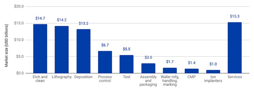
Introduction and Overview

The half-trillion-dollar semiconductor supply chain4 is one of the world’s most
complex. The production of a single computer chip often requires more than
1,000 steps passing through international borders 70 or more times before
reaching an end customer.5 However, the advancement of China’s
semiconductor industry could reconfigure these supply chains, affecting
international security and the competitiveness of current incumbents. Policies
that affect even a single firm or supply chain step can have global ripple
effects with tens of billions of dollars of impact. To avoid unpredicted harms,
policymakers must understand the supply chain and national competitiveness
across each sector. This report aims to provide such an assessment. Though it
maps national competitiveness for all key countries and regions, it focuses on
China’s development in each sector. Except where otherwise noted, data
throughout this report is current as of 2019, and country and region market
shares are based on firm headquarters, rather than locations of operations.
However, firm headquarters may not fully capture national competitiveness.
For example, many U.S. firms keep significant operations in China and other
countries.

At a high level, the supply chain includes seven sectors (Figure 1).6

Figure 1: The semiconductor supply chain

Note: Blue: Supply chain segment; Purple: Business model for production

Research and development advances all sectors of the supply chain. It
includes pre-competitive, exploratory research on foundational technologies
and competitive research directly advancing the leading edge of
semiconductor technology.

                                Center for Security and Emerging Technology | 5
Production takes three major steps: design, fabrication, and assembly,
testing, and packaging (ATP). These steps either occur in a single firm—an
integrated device manufacturer (IDM) that sells the chip—or in separate
firms, where a fabless firm designs and sells the chip and purchases
fabrication services from a foundry and ATP services from an outsourced
semiconductor assembly and test (OSAT) firm. Production requires several
inputs: materials, semiconductor manufacturing equipment (SME),
electronic design automation (EDA), and core intellectual property (IP).
The following is a summary of production steps and how they use these
inputs.
Design involves specification, logic design, physical design, and validation
and verification. Specification determines how the chip should operate in the
system using it.7 Logic design creates a schematic model of interconnected
electrical components. Physical design translates this model to a physical
layout of electrical components and interconnects, the wires that connect
components. Validation and verification ensure chips based on the design will
operate as expected.8 EDA is software used to design chips. Until the 1970s,
when chips included few electric components, engineers drew designs
manually. Today, chips include billions of interconnected transistors and other
electrical components. To manage this complexity, chip designers use EDA
software’s automated design tools.9 Core IP consists of reusable modular
portions of designs,10 allowing design firms to license and incorporate them in
their designs.
Fabrication turns designs into chips, relying on various SME and materials.
First, a furnace forms a cylinder of silicon (or other semiconducting materials),
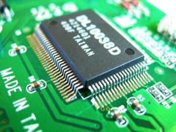
which is then cut into disc-shaped wafers (first image in Figure 2).
Semiconductor fabrication facilities (“fabs”) make chips in these wafers in two
steps: forming transistors and other electrical devices in material layers within
the silicon; and forming metal interconnects between the electrical devices in
insulating layers above the silicon.11 Together, the electrical devices and
interconnects form circuits. A chip may contain dozens of layers in total. What
follows is an example of how to form a single layer. First, “deposition” tools
add a film of material that will form the basis of a new permanent layer. Then,
a process called “photolithography” draws circuit patterns in the layer,
starting with coating a “photoresist” on the deposited material. A
photolithography tool passes light through a “photomask”—a transparent
plate with a circuit pattern—to transfer that pattern to the photoresist.
(Photomasks are themselves made with lithography tools.) The light dissolves
Center for Security and Emerging Technology | 6parts of the photoresist according to the circuit pattern. “Etching” tools carve
the newly created pattern in the photoresist into the permanent layer below
the photoresist. The photoresist is subsequently removed and the etched
material cleaned off of the layer. (Other times, instead of etching, atoms are
embedded into the layer in a process called “ion implantation.”) Then, the
completed layer is flattened (in a process called “chemical mechanical
planarization”) to allow a new layer to be added, and the process begins
again.12 Throughout fabrication, “process control” tools inspect the wafer and
its layers to ensure no errors.
Assembly, testing, and packaging starts with cutting a finished wafer—which
contains dozens of chips in a grid pattern after fabrication (second image in
Figure 2)—into separate chips. Each chip is mounted on a frame with wires
that connect the chip to external devices, and enclosed in a protective casing.
This produces the final look of a dark gray rectangle with metal pins at the
edges (third image in Figure 2). The chip is also tested to ensure it operates as
intended. ATP also requires various SME and materials.
The above description oversimplifies the technical process, but conveys the
high-level steps involved. In reality, each individual step is highly complex,
requiring several sub-steps. And the atomic precision of the fabrication
process requires clean rooms clear of dust particles, which can interfere with
chip fabrication.
End use involves distribution of chips for integration into products—
smartphones, laptops, servers, communications equipment, and automobiles,
among others.13
Figure 2: The chip manufacturing process
New wafer → Chips fabricated in wafer → Packaged chip
Firms headquartered in six countries and regions control virtually the entire
supply chain. Table 1 presents CSET estimates of the contribution to
semiconductor value of each supply chain segment (in purple). These values
Center for Security and Emerging Technology | 7add to 100 percent. See Appendix A for calculations of value add for each
supply chain segment. It also presents regional market shares of supply chain
segments (in green). Table 1 also provides each region’s total value add to
the global supply chain (in blue). Each of these values is a weighted average
of a region’s market shares across all supply chain segments. The weighting is
each segment’s weighted by sectoral value add. Because of lack of data,
Table 1 excludes fab materials besides wafers (4.1 percent value add), and
packaging materials (3.5 percent value add). The former are typically
purchased by fabs; the latter by ATP facilities. For this reason, the value of
non-wafer fab materials and packaging materials are incorporated into “fab”
and “ATP,” respectively. The United States is the world leader overall, while
South Korea, Japan, Taiwan, and Europe (especially the Netherlands, U.K.,
and Germany) contain world-leading firms in other advanced segments.
Table 1: Semiconductor value add and market shares by segment and firm
headquarters
Market shares
Segment
Value add U.S. S. Korea Japan Taiwan Europe China Other
EDA 1.5% 96%for third-party customers, unlike U.S.-based Intel, whose leading-edge logic
fabs make chips based on Intel’s own chip designs.) However, these
capabilities are all dominated by U.S. allies. Taken together, the United States
and its allies are internationally competitive in every segment in the supply
chain—in short, adding allies would turn all of Table 2 green.
Center for Security and Emerging Technology | 9Table 2: The United States’ competitiveness across supply chain segments
R&D Lithography tools Assembly & pkg tools CMP tools
EUV scanners Assembly inspection
Design ArF immersion scanners Dicing Ion implanters
Logic chips ArF dry scanners Bonding Low current
CPUs (logic) KrF steppers Packaging High current
GPUs (logic) i-line steppers Integrated assembly High voltage
FPGAs (logic) Mask aligners Ultra high dose
AI ASICs (logic) E-beam lithography Testing tools
DRAM (memory) Laser lithography Memory EDA software
NAND (memory) Imprint lithography System-on-a-chip
Analog chips Imprint lithography Burn-in Core IP
OSD Resist processing Linear & discrete
Handlers & probers Raw Materials
Fab Deposition tools
Logic chips Chemical vapor deposition Wafer and mask tools Fab materials
Logic foundry Physical vapor deposition Wafer manufacturing Wafers
Logic IDM Rapid thermal processing Wafer & mask handling Photoresists
Advanced logic Tube-based diffusion & dep. Wafer marking Photomasks
Memory chips Spin coating CMP slurries & pads
Analog chips Electrochemical deposition Process control tools Deposition
Optoelectronics Wafer inspection Electronic Gases
Sensors Etch & clean tools Photomask inspection Wet chemicals
Discretes Dry etch and clean Wafer level pkg inspect.
Atomic layer etch Process monitoring Packaging materials
ATP Wet etch and clean
Note: Green: high capabilities (internationally competitive); Yellow: moderate capabilities;
Orange: low capabilities; Red: minimal or no capabilities; Bolded: high-level category;
Unbolded: items within and listed below high-level category. Ratings based on authors’
analysis, as summarized in the following sections.
Center for Security and Emerging Technology | 10China lags behind overall, but is progressing in some segments (Table 3).15 It
excels in ATP, tools for assembly and packaging, and raw materials. It has
moderate and growing capabilities in design, fabrication, CMP tools, and
some etch and clean tools. China faces challenges in other segments,
including most SME. Its greatest weaknesses are in EDA, core IP, some fab
materials (especially photoresists), leading-edge logic fab capacity, and
certain SME. These SME include lithography tools (most importantly, extreme
ultraviolet scanners and argon fluoride immersion scanners), process control
tools, testing tools, atomic layer etch, wafer and mask handling tools,
advanced deposition tools, and some ion implanters. These weaknesses—
where China has low, minimal, or no capabilities according to Table 3—are
“chokepoints.” They involve items necessary for advanced chip production
exclusively produced by the United States and its allies.16
Table 3: China’s competitiveness across supply chain segments
R&D Lithography tools Assembly & pkg tools CMP tools
EUV scanners Assembly inspection
Design ArF immersion scanners Dicing Ion implanters
Logic chips ArF dry scanners Bonding Low current
CPUs (logic) KrF steppers Packaging High current
GPUs (logic) i-line steppers Integrated assembly High voltage
FPGAs (logic) Mask aligners Ultra high dose
AI ASICs (logic) E-beam lithography Testing tools
DRAM (memory) Laser lithography Memory EDA software
NAND (memory) Ion beam lithography System-on-a-chip
Analog chips Imprint lithography Burn-in Core IP
OSD Resist processing Linear & discrete
Handlers & probers Raw Materials
Fab Deposition tools
Logic chips Chemical vapor deposition Wafer and mask tools Fab materials
Logic foundry Physical vapor deposition Wafer manufacturing Wafers
Logic IDM Rapid thermal processing Wafer & mask handling Photoresists
Advanced logic Tube-based diffusion & dep. Wafer marking Photomasks
Center for Security and Emerging Technology | 11Memory chips Spin coating CMP slurries & pads
Analog chips Electrochemical deposition Process control tools Deposition
Optoelectronics Wafer inspection Electronic Gases
Sensors Etch & clean tools Photomask inspection Wet chemicals
Discretes Dry etch and clean Wafer level pkg inspect.
Atomic layer etch Process monitoring Packaging materials
ATP Wet etch and clean
Note: Green: high capabilities (internationally competitive); Yellow: moderate capabilities;
Orange: low capabilities; Red: minimal or no capabilities; Bolded: high-level category;
Unbolded: items within and listed below high-level category. Ratings based on authors’
analysis, as summarized in the following sections.
Each following section covers each country and region’s national
competitiveness (with extra focus on China) in each segment in detail—R&D,
production (design, fabrication, and ATP), SME, EDA, core IP, and materials.
(This report does not further discuss distribution and end use of
semiconductors.) Although the following sections can be read in order,
readers can view each section separately for an overview of that segment.
Appendix B includes a glossary of terms.
Research and Development
The United States decisively leads all other countries—including China—in
semiconductor R&D, which feeds into all other supply chain segments. The
private sector performs most semiconductor R&D.
Figure 3 breaks down semiconductor industry R&D by firm headquarters.
Globally, the semiconductor industry spent $64.6 billion on R&D in 2018
after a compound annual growth rate of 3.6 percent per year between 2013
and 2018.17 The U.S. semiconductor industry held a commanding lead with
$39.8 billion in R&D spending in 2019,18 with five of the top 10
semiconductor firms by R&D spending in 2018.19 By comparison, Chinese
semiconductor firms spent only $2.6 billion in semiconductor R&D in 2018.20
Countries excluded from Figure 3 account for an insignificant portion of
semiconductor industry R&D. Industry R&D is mostly proprietary, but many
semiconductor firms partner with competitors for R&D. One survey of 12
major semiconductor firms found nearly 200 research collaborations.21
Center for Security and Emerging Technology | 12Figure 3: U.S. firms led semiconductor industry R&D in 2018
Source: SIA, SemiWiki22
The U.S. semiconductor industry spends the highest percentage of
semiconductor sales on R&D at 16.4 percent, with China at 8.3 percent
(Figure 4).
Figure 4: U.S. semiconductor firms had greater R&D intensity than
counterparts in 2019
Source: SIA23
Governments of the United States, South Korea, Japan, Taiwan, and the
Netherlands play a minor role in semiconductor R&D.24 In 2019, the U.S.
government spent $6 billion on semiconductor R&D. This amount includes
$1.7 billion directly for the semiconductor sector and $4.3 billion on related
technology sectors (such as engineering, computer science, mathematics, and
the physical sciences).25 Besides direct R&D funding, many governments
subsidize semiconductor firms either with R&D tax breaks26 or other funding—
Center for Security and Emerging Technology | 13below-market financing and tax breaks for capital investment and corporate
income—that firms can redirect to R&D.27
By comparison, the Chinese government subsidizes its semiconductor industry
with about $15 billion per year.28 These subsidies are far greater as a
percentage of recipient firm revenues than government subsidies to any other
countries’ firms. However, China’s subsidies are similar in absolute amounts to
those provided by many other governments, as the globally leading
semiconductor firms produce much greater revenue than do China’s
semiconductor firms. Moreover, China’s R&D tax breaks are only a small
fraction of its total subsidies—much smaller in absolute terms than U.S. R&D
tax breaks.29
Production
The United States, South Korea, Europe, Japan, Taiwan, and China are the
key countries and regions designing, fabricating, assembling, testing, and
packaging semiconductors. In 2019, semiconductor production accounted
for $412.3 billion in sales, with logic and memory chips taking the biggest
shares (Figure 5).
Figure 5: 2019 semiconductor market
Source: WSTS30
Note: Logic chips include microprocessors and microcontrollers.
Semiconductors are produced under two business models.31 In the
“integrated device manufacturer” model, the same firm (an IDM) performs all
three production steps. In the “fabless-foundry” model, different firms perform
each step. Fabless firms design and sell the chips,32 but buy manufacturing
services from foundries and assembly, test, and packaging services from
outsourced semiconductor assembly and test (OSAT) firms.33 IDMs typically
Center for Security and Emerging Technology | 14produce memory chips, analog chips, and optoelectronics, sensors, and
discretes (OSD), while logic chips are produced under both models. Figures
6 and 7 show chip sales and country shares by business model.
Figures 6 and 7: Chip sales and country shares by business model
Sources: SIA, IC Insights, Yole, CSET estimates34
The following subsections analyze regional competitiveness for design,
fabrication, and ATP. Each subsection incorporates data for both IDMs and
firms operating under the fabless-foundry model.
Design
The United States, South Korea, Europe, Japan, Taiwan, and China perform
almost all of the world’s semiconductor design. The United States leads in
logic and analog chips, South Korea in memory chips, and Europe in
discretes. China designs many logic chips—though most of its chips do not
compete with state-of-the-art U.S. chips—and some discretes; it is also
beginning to design memory chips (Figure 8 and Table 4). (The market shares
and sizes are for semiconductor sales, which include value-add from steps
besides design. However, because the same firm typically designs and sells a
semiconductor—even if it often outsources fabrication and ATP—these market
shares correlate well with shares in design activities.) This section focuses on
certain high-end logic chips and the most common memory chips.
Center for Security and Emerging Technology | 15Figure 8: 2019 design shares by type and firm headquarters
Sources: SIA, IC Insights, TrendForce, financial statements35
Note: China has a small share (Memory DRAM $62.9 billion Samsung (South Korea), SK Hynix Moderate:
released in 2020) contains approximately double the transistor density as a
previous node (e.g., “7 nm” released in 2018) and is also more cost-
effective.49 Finally, Phytium produces a 28 nm CPU based on Arm’s
architecture for supercomputers.

Chinese CPUs have few civilian customers,50 reflecting their lack of
competitiveness on the open market. China’s large businesses depend on
imports for 95 percent of the CPUs they consume.51 The country remains
especially weak on CPUs with the x86 architecture, for which U.S. firms have
a captive customer base.

Discrete graphics processing units. GPUs have long been used for graphics
processing and in the last decade have become the most used chip for
training AI algorithms.52 The United States monopolizes the design market for
GPUs, including standalone “discrete GPUs,” the most powerful GPUs. Two
U.S. firms, Nvidia and AMD, dominate the discrete GPU market.53 U.S.-
based Intel is also developing a discrete GPU.54 China’s only significant GPU
firm is Jingjia Micro, selling largely to military customers.55 However, its sales
totaled only $36 million in 2019, and its GPUs are produced at the
substandard 28 nm node.56

Field-programmable gate arrays. FPGAs, unlike other chips, can be
reprogrammed after deployment to suit specific calculations, such as
executing AI algorithms (also called “inference”). U.S. firms capture virtually
the entire FPGA design market.57 China’s three FPGA-makers largely
manufacture at very old nodes, between 40 and 55 nm.58 An exception is
Efinix’s development of a 10 nm “eFPGA,” a stripped-down version of an
FPGA whose designs can be incorporated into other chips.59 On balance,
China’s FPGAs are not competitive with U.S. counterparts.

Application-specific integrated circuits for artificial intelligence. AI ASICs
often achieve greater speed and efficiency for artificial intelligence than
GPUs and FPGAs, but are usable only for specific AI algorithms.60 From
2017 to 2019, most of the venture capital investment in fabless firms went to
AI chip design startups.61 More firms are developing these chips and China
has advanced the most, as ASICs can be easier to design than CPUs, GPUs,
and FPGAs.62 Still, few highly specialized ASICs have been widely
commercialized, as their markets are often too small for recouping fixed
development costs. China does best with AI inference ASICs, though its firms
are also developing AI training ASICs. A notable example of the latter is
Huawei’s Ascend 910, fabricated at TSMC’s 7 nm node and competitive

                            Center for Security and Emerging Technology | 18
with leading firms.63 However, Huawei’s chip designs license foreign IP from
the U.K.-based, Japanese-owned ARM.
Memory chips. Memory chips store the digital data on which logic devices
perform calculations. DRAM provides “volatile” storage of data while a
computer operates, but loses it when the computer powers down. By contrast,
NAND flash memory is “non-volatile,” storing memory permanently. South
Korea, the United States, and Taiwan control the market for DRAM design,
while South Korea, the United States, and Japan do for NAND flash memory.
China is attempting to produce DRAM and NAND chips as well. These chips
comprise 98 percent of the memory chip market.64 Although Chinese firms
currently account for only a small amount of memory chip production,
ChangXin is developing capacity to produce 3 percent of the world’s DRAM
output and YMTC to produce 5 percent of the world’s NAND flash memory
output.65 Memory chips are more commoditized and easier to produce than
logic chips, and producers mostly compete on price—a strategy at which
Chinese firms excel. A larger barrier is access to patent licenses from industry
leaders,66 though Chinese memory chip suppliers are acquiring them.67
Therefore, memory chip design is unlikely to remain a major chokepoint for
China.68
Fabrication
Firms headquartered in the United States, Taiwan, South Korea, Japan, and
China control the vast majority of the world’s fab market share (Figure 9) and
fab capacity (Figure 10 and Table 5)—most of which is also physically
located in these countries (Figure 11). There are two business models for fabs:
(1) fabs owned by IDMs, which manufacture chips based on their own
designs; and (2) foundries, i.e., fabs operating independently and
manufacturing chips for third-party customers. However, although China’s
shares look strong, much of that capacity is aspirational (suffering from low
yields and utilization) and at older nodes. Many of these fabs stay online with
the help of state support, receiving subsidies far greater as a percentage of
revenue than any leading fabs.69 Foreign chipmakers operate the most
advanced and reliable fabs in China and generate more revenue than the
country’s chipmakers.70
Advanced logic capacity represents China’s greatest weakness in fabs,
though it is attempting to build such capacity. Additionally, logic chips (e.g.
CPUs, GPUs, FPGAs, and AI ASICs) are especially critical for applications
Center for Security and Emerging Technology | 19relevant to national and international security. The remainder of this section
therefore focuses on logic fab capacity.
Figure 9: 2019 market share by fab type and firm headquarters
Sources: CSET calculations, IC Insights, SIA, SEMI, WSTS71
Figure 10 shows fab capacity shares by firm headquarters for several
categories. These categories include capacity for all semiconductors, logic
chips (including capacity held by both foundries and IDMs), memory chips,
analog chips, optoelectronics, sensors, and discretes. A more detailed
breakdown is provided for logic chips. Specifically, Figure 10 includes logic
chip capacity respectively held by IDMs and foundries, as well as logic chip
capacity (held by both foundries and IDMs) at or below the 45 nm node.
Figure 10: 2020 wafer fab capacity by fab type and firm headquarters
Source: “World Fab Forecast,” SEMI, November 2020 edition72
Center for Security and Emerging Technology | 20Figure 11 shows fab capacity shares by fab location, broken down
according to the same categories as in Figure 10.
Figure 11: 2020 wafer fab capacity by fab type and fab location
Source: “World Fab Forecast,” SEMI, November 2020 edition
Table 5: 2019 fab market and Chinese competitiveness
Fab type73 Fab capacity Top firms + Chinese firms Chinese firm Chinese
share capabilities HQ fab
share
Foundry Logic 28% TSMC (Taiwan), Samsung Moderate: small 21%
chips (South Korea), Global amount of low-yield
Foundries (U.S.), SMIC 14 nm capacity
(China), UMC (Taiwan),
Powerchip (Taiwan), Hua
Hong (China), others
IDM 6% Intel (U.S.), Renesas (Japan), Low: Minimal 2%
STMicroelectronics capabilities
(Switzerland), Microchip
(U.S.), NXP
(U.S./Netherlands), Toshiba
(Japan), others
Memory 32% SK Hynix (South Korea), Moderate: capacity 8%
chips74 Samsung (South Korea), developing but largely
Micron (U.S.), Toshiba aspirational
Center for Security and Emerging Technology | 21IDM, (Japan), Western Digital
cont’d (U.S.), Intel (U.S.), YMTC
(China), ChangXin (China),
others
Analog 7% Texas Instruments (U.S.), ON Moderate 7%
chips (U.S.), SiEn (China), ASMC
(China), Bosch (Germany),
STMicroelectronics
(Switzerland), TowerJazz
(Japan), others
Opto- 7% Sony (Japan), Nichia (Japan), High 27%
elec- Samsung (South Korea),
tronics Osram (Germany), HC
SemiTek (China), Epistar
(Taiwan), Sanan (China),
Aucksun (China), Changelight
(China), others
Sensors 2% Qorvo (U.S.), Broadcom Moderate 9%
(U.S.), Seagate (U.S.), Texas
Instruments (U.S.), OmniVision
(China), SMIC (China), others
Discrete 12% Infineon (Germany), High 28%
STMicroelectronics
(Switzerland), Hangzhou
(China), ON (U.S.), Mitsubishi
(Japan), AOS (U.S.), CR
(China), Yangzhou (China),
others
Firms headquartered in the United States, Taiwan, South Korea, Japan, and
China control most of the world’s logic capacity—and also keep most of it
within their borders. Foundries control more than 80 percent of the world’s
logic fab capacity (Table 5). Three firms – headquartered in the United States
(Intel), Taiwan (TSMC), and South Korea (Samsung) – control virtually all of
the world’s advanced logic fab capacity (≤10 nm), though U.S.-based Intel is
building such capacity in Israel and Ireland.75
Winner-take-all dynamics pose challenges to follow-on competitors in the
logic foundry industry. Market leader TSMC has 54 percent of the world’s
logic foundry market share and an even larger market share for leading-edge
logic foundries.76 Now it produces state-of-the-art 5 nm node chips and is
Center for Security and Emerging Technology | 22rapidly increasing revenue per wafer while other chipmakers operating
foundries are seeing declines—including U.S.-based GlobalFoundries,
Taiwan-based UMC, and China’s most advanced chipmaker, SMIC.77
Samsung is also introducing 5 nm logic foundry capacity, while Intel is
fabricating 10 nm logic chips with specifications competitive with TSMC’s 7
nm node chips.78 The United States has strong capacity, though its most
advanced logic foundries, held by GlobalFoundries, are at 12 nm. U.S.-
based IDM Intel still plans to introduce 7 nm node chips with specifications
competitive with TSMC’s 5 nm node chips, but is falling behind, with plans to
introduce them by 2022 or early 2023.79
Because of minimal and low quality leading-edge capacity, Chinese
foundries face difficulty attracting foreign fabless customers.80 SMIC has
reached 14 nm, but at a capacity of only 6,000 wafers per month (0.2
percent of the world’s ≤16 nm logic fab capacity), with plans to increase to
35,000 (1 percent).81 Chinese chipmaker Hua Hong is also attempting to
develop 14 nm capacity.82 To compete with TSMC, Chinese foundries must
overcome know-how deficits and rely on subsidies to invest in leading-edge
capacity—whose costs rise quickly from one node to the next.83 If applied,
future U.S., Japanese, and Dutch export controls on SME and materials could
prevent Chinese foundries from building advanced capacity. The current
Dutch ban on exports of EUV scanners to China already prevents it from
building capacity more advanced than 7 nm.84
Assembly, Testing, and Packaging
ATP occurs under two business models: (1) as in-house ATP services
performed by integrated device manufacturers (IDMs) and foundries after
fabrication; and (2) by outsourced semiconductor assembly and test (OSAT)
firms, which perform ATP for third-party customers. ATP is labor-intensive and
lower value than design and fabrication, and does not develop skills in these
two segments. Therefore, firms historically set up ATP facilities in developing
countries.85
Firms headquartered in Taiwan, the United States, China, and South Korea
are the main providers of ATP services (Figure 12 and Table 6). China
benefited from offshoring, developing a strong ATP industry—its OSAT
industry is the world’s second largest after Taiwan. Additionally, non-Chinese
IDMs keep many ATP facilities in China. Although the top three ATP firms in
China are Chinese OSATs, the rest of the top 10 are non-Chinese IDMs (six
Center for Security and Emerging Technology | 23American).86 Therefore, ATP is arguably a supply chain vulnerability for the
United States. Overall, 22 percent of the world’s ATP facilities are in China.87
Although ATP was historically low value, packaging has increasingly become
a bottleneck on chip performance.88 Densities of transistors in logic and
memory units in chips have continued to increase exponentially, but the
density of interconnects between logic and memory—governed by
packaging—have increased at a much slower rate, leading to communication
bottlenecks between chips.89 Additionally, the rates of increases in density of
logic and memory may slow,90 providing comparatively more innovation
opportunities for advanced packaging.91
Figure 12: Country market shares by firm headquarters
Source: Yole, SIA, SEMI, IC Insights, WSTS, CSET calculations92
Table 6: ATP market and Chinese competitiveness
Sector 2019 market Top firms + Chinese firms Chinese firm 2018
size capabilities Chinese
market share
Outsourced $28 billion ASE (Taiwan), Amkor (U.S.), JCET High 21%
semiconductor (China), Powertech (Taiwan),
assembly and test TongFu (China), Tianshui (China),
UTAC (Singapore), others
In-house ATP (by $25 billion Intel (U.S.), Samsung (U.S.), S.K. Minimal 6%
foundries and Hynix (South Korea), Micron (U.S.),
IDMs)93 TSMC (Taiwan), others
Center for Security and Emerging Technology | 24Semiconductor Manufacturing Equipment
The United States, Japan, and the Netherlands dominate the production of
SME, the most severe chokepoint in China’s chip supply chains. There are
dozens of categories of SME (Figures 13 and 14 present 2019 SME market
sizes and country shares by segment).94 “Services” include support services
provided by SME firms to help with setup, troubleshooting, and repair of any
SME. Most SME is used for making chips or inputs to them. These tools
include those for wafer manufacturing, wafer and photomask handling, wafer
marking, ion implantation, lithography, deposition, etch, clean, chemical
mechanical planarization, and process control. Specialized tools are also
used for assembly, testing, and packaging.
China has little to no market share in all major segments, except for assembly
and packaging tools.95 China’s most critical chokepoint is in lithography
tools—especially extreme ultraviolet (EUV) photolithography and deep
ultraviolet (DUV) photolithography, but also imprint lithography, e-beam
lithography, laser lithography, resist processing equipment, and photomask
inspection and repair tools. Other tools are also chokepoints, especially those
for advanced ion implantation, atomic layer etching, advanced chemical
vapor deposition, wafer and mask handling, wafer and photomask
inspection, and testing advanced logic chips. Companion CSET policy briefs
titled “Securing Semiconductor Supply Chains”96 and “China’s Progress in
Semiconductor Manufacturing Equipment”97 offer recommendations on
export controls and other policies affecting SME that could slow China’s
development in indigenizing both SME and leading-edge chipmaking
capacity.
Figure 13: 2019 SME market by SME type
Source: VLSI Research
Center for Security and Emerging Technology | 25Figure 14: 2019 SME country shares by firm headquarters
Source: VLSI Research
Wafer Manufacturing, Wafer Marking, and Handling
Japan, the United States, and Austria are key producers of wafer
manufacturing, handling, and marking equipment. (Figure 15 and Table 7).
China’s producers have minimal capabilities and market share. Given their
higher value, wafer manufacturing equipment and handling systems are
chokepoints for China.
Center for Security and Emerging Technology | 26Figure 15: 2019 wafer manufacturing, wafer marking, and handling country
shares by firm headquarters
Source: VLSI Research
Table 7: 2019 wafer manufacturing, wafer marking, and handling market
and Chinese competitiveness
Equipment 2019 Top firms + Chinese firms Chinese firm Chinese
market capabilities market share
size
Wafer mfg. Crystal $21 PVA TePla (Germany), JSG LowPhotomask $99 Brooks (U.S.), Daifuku (Japan), 0%
handling million Gudeng (Taiwan), RECIF
(France)
Wafer marking systems $500 ESI (U.S.)
thousand
Crystal growing furnaces and machining tools are necessary to produce all
wafers—thin, disc-shaped materials fabs used to produce chips.98 These tools
have relatively lower value and complexity relative to other SME. Japan,
Germany, and Switzerland are the main producers, while China has a few
insignificant producers and relies on imports.99
Wafer bonders and aligners join silicon wafers, often after chips are
fabricated in the wafers. Austria, Germany, and the United States produce
this equipment, while China does not. Shanghai Micro Electronics Equipment
(SMEE) markets these tools, but has minimal sales and capabilities.100
Wafer and photomask handlers store and transport wafers and photomasks
in a fab. Photomasks are transparent plates containing a circuit pattern that
photolithography tools pass light through to transfer the pattern to the chip.
Japan, South Korea, Taiwan, and France produce wafer and photomask
handlers, which China does not produce. It is unclear whether this is an
important chokepoint for China, as the tools are not as complex as other
SME; thus, China may eventually produce them.
Wafer marking systems mark wafers, or chips manufactured in wafers, with
identifiers using a laser. The United States solely produces this equipment.
However, other countries, including China, could readily develop this
technology given its low complexity and expense.
Ion Implanters
Ion implanters embed dopants into silicon wafers to give different parts of the
wafer different levels of semiconductivity to make functional transistors in
chips.101 Four categories are needed for different use-cases.102 Low-to-
medium-current ion implanters and high-current ion implanters are most
commonly used, with high-current ion implanters capable of greater
throughput. High-voltage ion implanters can implant ions deeply into silicon.
Ultra-high-dose doping implanters can achieve greater dopant density than
the other tools.
Center for Security and Emerging Technology | 28The United States is the dominant producer of ion implanters, with Japan and
Taiwan rounding out most of global market share (Figure 16 and Table 8).
China produces a small amount of less-advanced ion implanters for
specialized purposes, but not ion implanters for leading-edge logic chips,
making it a moderate chokepoint. China has two minor producers. State-
owned defense conglomerate China Electronics Technology Group produces
a variety of ion implanters for discrete semiconductors and chips based on
silicon carbide and gallium arsenide103 with 28 nm capabilities104 and
estimated sales of $15 million per year.105 Kingstone Semiconductor
produces high-current ion implanters for photovoltaics.106
Figure 16: 2019 ion implanters country shares by firm headquarters
Source: VLSI Research
Table 8: 2019 ion implanters market and Chinese competitiveness
Equipment 2019 Top firms + Chinese firms Chinese firm Chinese
market size capabilities market share
Low to Medium $0.24 Applied Materials (U.S.), Nissin Low: ≥28 nm, usedLithography
The Netherlands, Japan, and a small number of other countries are the
dominant producers of lithography equipment, critical for the production of
chips and photomasks (Figure 17 and Table 9). China cannot produce any
advanced lithography equipment. Most importantly, the Netherlands and
Japan are exclusive providers of advanced photolithography equipment—
especially extreme ultraviolet (EUV) scanners and secondarily argon fluoride
(ArF) immersion scanners—necessary for mass-production of advanced chips,
representing China’s top chokepoint.
Figure 17: 2019 lithography country shares by firm headquarters
Source: VLSI Research
Table 9: 2019 lithography market and Chinese competitiveness
Equipment 2019 Top firms + Chinese firms Chinese firm Chinese
market capabilities market
size share
Photo- EUV $3.1 ASML (Netherlands) None 0%
lithography scanners billion
ArFi $5.8 ASML (Netherlands), Nikon (Japan) None: but
scanners billion developing 28
nm tool
ArF $0.78 ASML (Netherlands), Nikon (Japan), Moderate: 90
scanners billion SMEE (China) nm tool, but
limited
Center for Security and Emerging Technology | 30capabilities for
mass chip fab
KrF $0.96 ASML (Netherlands), Canon (Japan), Moderate:
steppers billion Nikon (Japan), SMEE (China) 110 nm tool,
but limited
capabilities for
mass chip fab
i-line $0.69 Canon (Japan), ASML (Netherlands), Moderate: 2.8%
steppers billion Nikon (Japan), Veeco (U.S.), SMEE 280 nm tool
(China), Institute of Optoelectronic used largely for
Technology (China), others packaging, not
chip fab
Mask $0.12 SUSS MicroTec (Germany), Toray None 0%
aligners billion (Japan), USHIO (Japan), EV Group
(Austria)
Electron- Chip- $20 Vistec (Germany), JEOL (Japan)
Beam lithography making million
Mask- $0.49 NuFlare (Japan), JEOL (Japan),
making billion Applied Materials (U.S.), Vistec
(Germany)
Laser lithography $85 Mycronic (Sweden), Heidelberg
million Instruments (Germany)
Ion beam Minimal Thermo Fisher (U.S.), Hitachi (Japan),
lithography 107
Zeiss (Germany), Tescan (Czechia),
JEOL (Japan), HORIBA (Japan),
Eurofins (Luxembourg), A&D (Japan),
Raith (Germany), FOCUS (Germany),
others
Imprint lithography $24 EV Group (Austria), Canon (Japan),
million Nanonex (U.S.), SUSS MicroTec
(Germany), Obducat (Sweden)
Resist processing (tracks) $2.1 Tokyo Electron (Japan), Screen Low: i-line, KrF, 0.7%
billion (Japan), SUSS MicroTec (Germany), and ArF, not
SEMES (South Korea), Kingsemi currently ArFi &
(China), Brewer Science (U.S.), Rite EUV
Track (U.S.)
Center for Security and Emerging Technology | 31Table 10 summarizes the capabilities of lithography tools. (It excludes resist
processing equipment, which complements lithography equipment.)
Photolithography tools are used in high-volume chip production, and
currently include six grades from most to least advanced by supported nodes:
EUV, deep ultraviolet (DUV)—which includes ArF immersion (also called wet
ArF or ArFi), ArF (also called dry ArF), and krypton fluoride (KrF)—i-line, and
mask aligners. An older grade, g-line, is no longer used. Other types of
lithography equipment are for specific, lower-volume chips or photomasks (e-
beam and laser) or are emerging areas of development for future mass chip
production (imprint).
Table 10: Lithography types
Type Photolithography Imprint Electron-beam Laser Ion
litho- lithography litho- beam
graphy graphy litho-
Mask Stepper Scanner graphy
aligner
g-line i-line DUV EUV
KrF ArF ArFi
Source (nm) Various 436 365 248 193 13.5
Node Trailing ≥1,000 ≥350 ≥150 ≥65 ≥7 ≥5 Competitive with advanced scanners
(nm)108
Uses mask Yes No (typically direct-write)
High volume Yes Future? No
Key use case Chips Photomasks Photomasks
and chips
Photolithography: scanners and steppers. The Netherlands and Japan
dominate the production of scanners and steppers—the photolithography
equipment needed to mass-produce chips. The United States and China have
small market shares in less advanced steppers. One Dutch firm, ASML,
exclusively produces EUV scanners, the most advanced photolithography
equipment. ASML and Japan-based Nikon exclusively produce ArF
immersion scanners, the next most advanced. Scanners and steppers produce
Center for Security and Emerging Technology | 32light that passes through a photomask to transfer previously created circuit
patterns in the photomask onto multiple wafers.109
This equipment is China’s top chokepoint due to its technical complexity and
expense. First, scanners are the only tools combining high precision (by
producing light with small wavelengths) and high throughput (by using
photomasks, as will be described in the following “Maskless lithography”
subsection). EUV scanners are necessary for mass-producing 5 nm node
chips, while EUV and ArF immersion scanners together are the only
lithography tools capable of mass-producing chips in the 28 to 7 nm node
range, with ArF immersion in predominant use for even 45 nm (Table 10).
Second, EUV and ArF immersion scanners are the most expensive110 tools
used in chip fabrication, taking an increasingly large share of chip fabrication
costs.111 With “100,000 parts, 3,000 cables, 40,000 bolts and 2 kilometers
of hosing,” an EUV scanner is more complex than any SME and a typical car,
which has tens of thousands of parts.112 These trends are also making markets
for photolithography more consolidated113 and profitable114 than for other
high-value SME. Third, they require the greatest precision, being responsible
for drawing the nanoscale circuit patterns in chips. Fourth, EUV scanners
simplify and reduce the need for non-lithography fabrication steps,115 further
increasing photolithography’s importance relative to other SME.116 For these
reasons, improvements in photolithography also constrain Moore’s Law
improvements in transistor density—spurring the leading chipmakers Intel,
Samsung, and TSMC to preferentially invest in ASML to support its EUV
R&D.117
China is developing scanners and steppers. Shanghai Micro Electronics
Equipment (SMEE) has purportedly developed a 90 nm ArF tool and plans to
introduce a 28 nm ArF immersion tool by 2021 or 2022.118 Still, even if these
reports are true and the tools work, building a mass-production-ready tool
with low cost, low manufacturing error rates, and high throughput can take
years after initial prototyping.119 Even Chinese fabs are not yet using SMEE’s
90 nm steppers for mass chip production. Instead, SMEE’s photolithography
tools are used for the less difficult step of chip packaging (not fabrication),120
and mostly not for advanced packaging techniques.121 Besides SMEE, in
2018, China’s state media reported that the Institute of Optoelectronic
Technology in the Chinese Academy of Sciences developed an experimental
photolithography tool with a 365 nm i-line light source that achieves 22 nm
resolution and in the future could achieve 10 nm.122 This resolution capability
is inconsistent with known i-line technology, so the report is likely not credible.
Center for Security and Emerging Technology | 33Finally, some Chinese research institutes are attempting to develop
components for EUV, but it is unclear whether they will succeed.123
Photolithography: mask aligners. Only Germany, Japan, and Austria
produce mask aligners. Mask aligners are an alternative form of
photolithography where—unlike scanners and steppers—the wafer and
photomask remain in fixed relative position, either in direct physical contact or
in close proximity. However, this form of photolithography does not achieve
small feature sizes competitive with scanners and steppers.124 Therefore, mask
aligners only have special use-cases, are low value, and lack strategic
importance.
Maskless lithography: electron-beam, laser, and ion beam. Only Japan,
Germany, the United States, and Sweden produce electron-beam (e-beam)
and laser lithography tools, representing a critical chokepoint for China for
photomask production. These countries and others also produce ion beam
lithography tools, which could be used for photomask production (but rarely
are). Laser lithography tools (like photolithography tools) draw patterns with
light beams. By contrast, e-beam and ion beam lithography tools draw
patterns with electrons and ions, respectively.125 These tools can achieve
similar resolution as advanced photolithography tools.126 The key difference
is that e-beam, laser, and ion beam lithography tools do not use masks. The
advantage is that these tools can quickly and cheaply make new patterns
without a new mask. The disadvantage is that drawing patterns is slow
without a mask. Therefore, e-beam, laser, and ion beam lithography tools can
cost-effectively produce low-volume items like photomasks used with
photolithography tools. (Far fewer photomasks are needed than chips,
because a small number of photomasks are used to produce a large number
of chips during photolithography.) But these tools are ill-suited to mass chip
production given their low throughput. E-beam tools are the dominant tools
for photomask production, with laser lithography tools a distant second, and
ion beam lithography tools rarely used. Besides photomasks, about 4 percent
of the e-beam tool market is used for low-volume chip production (Table 9),
while laser lithography tools are not normally used for chip production.
Imprint lithography. Today, Austria is the main seller for semiconductor
applications, while Japan, the United States, and Germany are either selling
or developing for various other applications. Imprint lithography is a
potentially important chokepoint for China, as it could compete with
photolithography in mass chip production. Imprint lithography can achieve
Center for Security and Emerging Technology | 34leading-edge, nanoscale resolutions—and therefore is often called
nanoimprint lithography. It also uses a template, which plays a similar role as
a photomask in photolithography. The template contains a pattern that is
transferred to a wafer. Given its use of a template, imprint lithography can
theoretically achieve high-volume production. However, it has low yields and
produces too many defects to compete with photolithography.127 The main
firm selling it today for semiconductors, EV Group, has small sales geared
toward narrow use-cases. Toshiba plans to use Canon’s nanoimprint
technology to make 3D NAND memory chips.128 SUSS MicroTec, Nanonex,
and Obducat are also producers.
Resist processing. Japan is a dominant producer of resist processing tools
(also called “tracks”). Germany, South Korea, the United States, and China
each have small market shares. However, only Japan is the key producer of
the most advanced tracks for EUV and ArF immersion photolithography.129
Photoresists are chemicals deposited on a wafer that, when exposed to
patterned light that has passed through a photomask, selectively dissolve to
form the circuit pattern. Etching is then performed in places where the
photoresist has dissolved to transfer the circuit pattern permanently onto the
wafer. Resist processing tools coat photoresists on wafers (typically by spin-
coating, which spins the wafer to spread deposited photoresist), develop
them (dissolve portions hit by light), and bake them (harden undissolved
photoresist to prepare for etching). China’s only firm, Kingsemi, produces
tracks for ArF, KrF, and i-line photolithography, and claims it will develop
EUV and ArF immersion tracks by 2022.130 However, Kingsemi also
purportedly supports ≥28 nm nodes, which is normally in the ArF immersion
range.131 Because China does not currently produce tracks for EUV or more
advanced ArF immersion photolithography, these tracks are currently a
chokepoint for China.
Deposition
The United States, Japan, the Netherlands, and South Korea are leading
providers of deposition tools, while China has a small but growing share in
certain deposition market subsectors (Figure 18 and Table 11). Still, China
has chokepoints across the board, such as for rapid thermal processing tools.
Deposition tools are used to deposit thin films of materials on a silicon wafer.
After lithography and etching, these films become different chip layers,
including for transistors, interconnects (wires), and other elements. The vast
majority of deposition tools are used for chip production, so the technology
Center for Security and Emerging Technology | 35You can also read