Understanding and Performing MIPI D-PHY Physical Layer, CSI and DSI Protocol Layer Testing
←
→
Page content transcription
If your browser does not render page correctly, please read the page content below
Understanding and Performing MIPI®
D-PHY Physical Layer, CSI and DSI
Protocol Layer Testing
Application Note

Introduction
Currently many technologies are used in designing mobile or       MIPI Alliance was formed to define the hardware and
portable devices. These current interfaces are not well defined   software interfaces that would bring standardization, improve
and are proprietary for each component or subsystem vendor.       interoperability and help reduce many of the drawbacks faced
This fragmentation in the interfaces has made it difficult to     by the mobile handset developers and manufacturers. With
quickly bring out mobile/portable products into the market        new MIPI technologies, all of the above problems are solved
with growing feature sets, higher performance, improved battery   better. These MIPI standards are expected to revolutionize the
life, re-usability, and smaller form-factors, at lower costs.     entire mobile industry.

MIPI is a registered trade mark of MIPI Alliance www.mipi.org.

Application Note

D-PHY/CSI/DSI Background
The MIPI Alliance defines D-PHY as a re-usable, scalable
physical layer for interfacing various components such as
cameras and displays to baseband processors in next
generation smartphones, tablets, and other portable devices.
Unlike many of the existing interfaces, D-PHY is unique
because it can switch between differential (High Speed) and
single-ended (Low Power) mode in real time depending on the
need to transfer large amounts of data or to conserve power
to prolong the battery life. The D-PHY interface is capable of
operating in simplex or duplex configuration with single data          Figure 1. Block diagram of a typical mobile device.
lane or multiple data lanes, giving a flexibility to avail the links
as needed. In addition, clock is always uni-directional (Master
to Slave) and is in quadrature phase with data.
This design complexity introduces some unique challenges
for testing and validating D-PHY based interfaces. Transmitter
validation for D-PHY designs requires accurate jitter and timing
analysis to the latest specifications coupled with minimal
testing times.
With the inclusion of high resolution displays and cameras
with the ability to capture or play high definition videos, the
amount of data transfer needed to achieve this high definition
functionality has increased tremendously. The Camera Serial
Interface (CSI-2) and the Display Serial Interface (DSI) are the
two packet-based high level protocols that carry image data
between the peripheral and the application processor. Both
these protocols use the D-PHY physical layer.

2   www.tektronix.com/mipi

Understanding and Performing MIPI® D-PHY Physical Layer, CSI and DSI Protocol Layer Testing

Figure 2. Modes and States in a D-PHY Data lane.

Figure 3. Modes and States in a D-PHY Clock lane.

Electrical Signal Challenges                                       In High Speed (HS) mode, the differential voltage is 140 mV
                                                                   min, 200 mV nominal, 270 mV max, with the data rate
A D-PHY interface can have a minimum configuration of one          extending up to 1 Gb/s. The HS mode consists of two
clock lane and one data lane, and a maximum configuration          possible states: Differential-0 (HS-0) and Differential-1 (HS-1).
of one clock lane and four data lanes. As shown in Figure 2,       In Low Power (LP) mode, the signaling is two single-ended
each data lane operates in one of two modes: High Speed            with 1.2 V swing operating at a maximum data rate of 10 Mb/s.
or Low Power. This means that the same two physical data           The LP mode consists of four possible states: LP-00, LP-01,
paths alternate between high speed differential signaling and      LP-10, and LP-11. In addition, the rise times in the HS mode
low power single-ended signaling.                                  are different from that of the LP mode.

                                                                                                           www.tektronix.com/mipi   3
Application Note
Some of the MIPI interfaces might operate at broadcast mode
where the signal will not be terminated at all, but the transmitter
continues to transmit the signal in broad cost mode.
During the transition of signal from single-ended to differential,
the impedance imbalance that occurs on the line which can
cause the glitch may be due to non-synchronous termination
transition between the TX and RX. In broad cost mode the
source impedance changes, but the Receiver impedance
remains open, so that you can see the glitch on the signal.
Most of the Global timing parameters must be measured
during the HS entry mode. These need to be performed
as Clock alone tests, data alone tests and Clock-to-data
tests. You also need to acquire the Cp, Cn and Dp, Dn
simultaneously, on separate channels of an oscilloscope
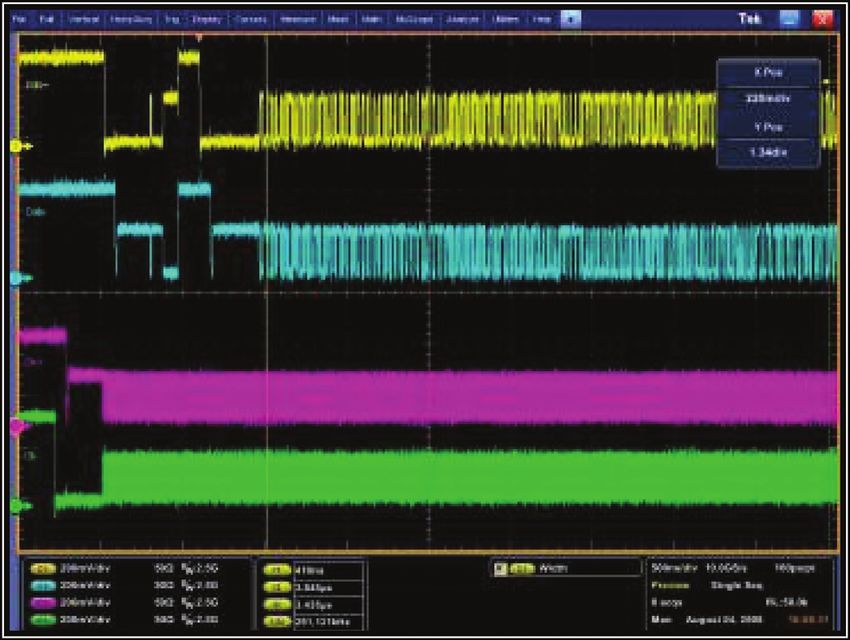
Figure 4. Pinpoint triggering. The probes that you use should be optimally chosen so that
its impact should be minimal on the signal for both single-
Most of the HS and LP measurements can be performed ended and differential operations. The probe should also be
while the signal transitions from HS mode to LP mode. The capable of capturing the activity on the bus during the transition.
oscilloscope’s trigger features enable you to acquire stable We use a differential probe so that it has minimal impact
transitions from HS mode to LP mode. As shown in Figure 4 during both non-terminated and terminated operations. Also,
screen capture, pinpoint triggering is used to trigger and it has minimal input capacitance so that its effect in low
capture the DP and DN transition edges, and the HS burst. frequency will not alter the signal rise time or fall time for both
the speed of operations.
Importance of Signal Integrity and The measurement algorithm is capable of tolerating the Glitch
Terminations as shown in Figure 4 when you operate in the broadcast mode
D-PHY operates at low speeds as well as at high speeds. and are still able to perform the measurement by selectively
At low speeds the signals are singled-ended, where the qualifying the HS entry mode.
other end is not terminated. At high speeds, the signals are
differential, but terminated during data transmission by the
Receiver automatically.
4 www.tektronix.com/mipi
Understanding and Performing MIPI® D-PHY Physical Layer, CSI and DSI Protocol Layer Testing

Figure 5. P7380 probe used with a probe-tip #020-3035-00 of P6780.

Signal Accessibility
The mobile designs are tiny in nature, with high packing
density. Probing these signals using any regular probe is a
challenging task. The signal traces cannot be extended at
ease to meet a specific choice of probe. To probe signals
from a miniature circuit, the probes with a wide range of
accessories like miniature tips, micro clips, solder-tips, etc are
needed. For example, a P7360 probe with square pin adapter,
and a probe-tip of P6780 (Partnumber 020-3035-00, kit of 15          Figure 6. Risetime measurements at various bandwidths.

tips) provides miniature accessibility and best fidelity.
The probes should be capable of supporting both HS and               Choice of Oscilloscopes
LP modes, with variance of different voltage levels, multiple
                                                                     The D-PHY bus data rates vary from 80 Mb/s to 1 Gb/s, with
speeds of operations and different terminations. Other
                                                                     typical implementations at 500 Mb/s. According to base or
recommended probes like P7225 can also be used to acquire
                                                                     conformance specifications, the rise times are no faster than
a D-PHY signal in broadcast mode.
                                                                     150 ps and no slower than 0.3 UI (Unit Intervals). For example,
The mobile/ portable devices also must be tested at extreme          to measure a 150 ps rise time of a signal (20 to 80 percent)
environmental conditions such as thermal chambers. In                using a flat-response oscilloscope to an accuracy of +/- 5
such cases, probes should provide sufficient long lead               percent would require a minimum of 3.2 GHz (1.2 x 0.4 /150
accessories such XL cables and probe tips that can sustain in        ps) bandwidth oscilloscope.
a temperature chamber.
                                                                     The screen capture in Figure 6 with a source of 148 ps
                                                                     indicates an oscilloscope with a bandwidth of 3.5 GHz
                                                                     onwards is sufficient for D-PHY signal measurements.

                                                                                                                        www.tektronix.com/mipi   5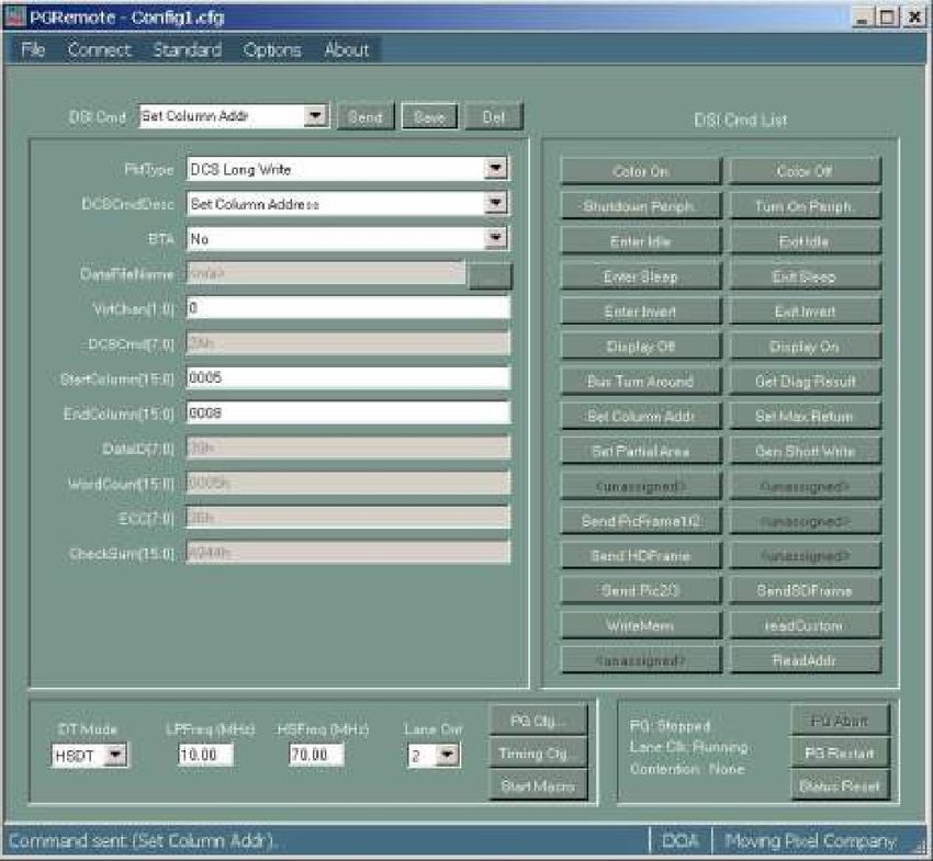
Application Note

                              Broadcast and Terminations
                              Before beginning of Data burst transmission, the High speed
                              data transmission happens in burst and it start with LP-01
                              state and end at stop state (LP-11) The minimum payload can
                              be as less as one of one byte where as the maximum payload
                              is protocol dependent.
                              During the start of transmission drivers get into HS-Rqst state
                              by driving the lane to LP01 state for the time TLPX, During
                              this interval, It is expected at the RX to change its termination
                              from High impedance to low impedance state. While testing,
                              It is not always possible to have TX and RX together for
                              example, device with MIPI interface may be forced to operate
                              in broad cast mode (Data is sent continuously) where the Rx is
                              not present. During the HS entry on these situation, the lanes
                              are switched to operate at expected termination, then there is
Figure 7.                     spike that occurs during the end of TLPX which might prevent
                              us to do the measurement of Thevanin low voltage at LP 00
                              state and other timings.
                              Tektronix D-PHY solutions designed with algorithms to
                              handling these scenarios as shown below, which are most
                              common during the debugging and the integration. You can
                              perform all the measurements related to HS timing during the
                              HS entry under these practical circumstances.

6    www.tektronix.com/mipi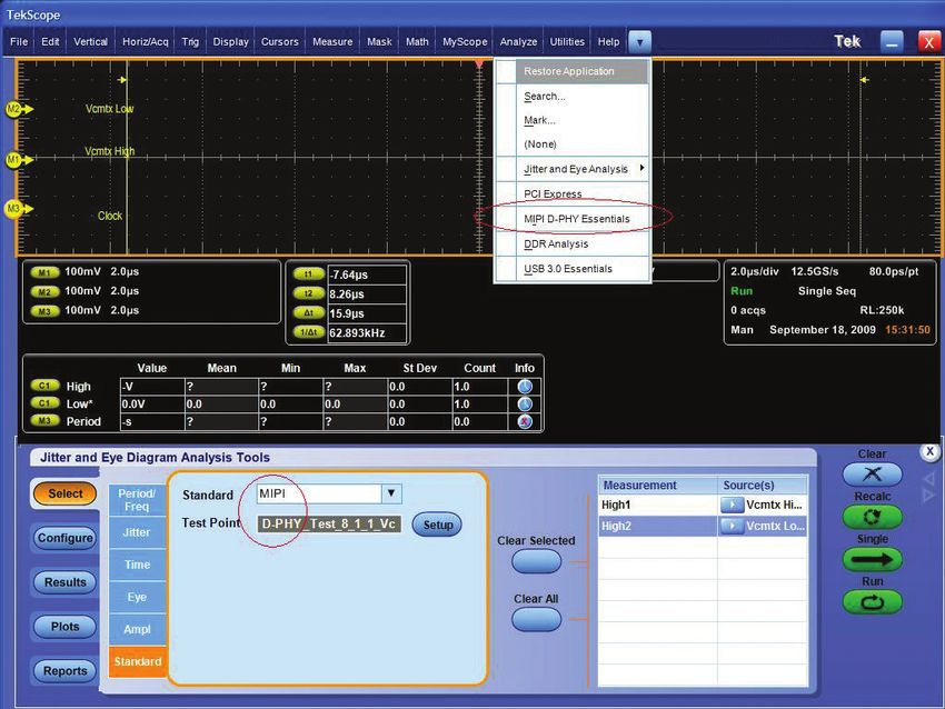
Understanding and Performing MIPI® D-PHY Physical Layer, CSI and DSI Protocol Layer Testing

Figure 8. D-PHYTX fully-automated solution.                        Figure 9. D-PHYTX test report.

Solution for D-PHY Testing                                         irrespective of lane terminations. D-PHYTX allows you to
                                                                   perform the measurements under in-circuit operations, along
TekExpress™ software with D-PHYTX option and chosen                with setup configurability, limits-editing, and customization for
oscilloscopes and probes provides a completely automated,          a DUT-specific data rate.
simple, and efficient way to test D-PHY signals, specifically
for Conformance and Verification.                                  The D-PHYTX reports not only provides Pass/Fail summary
                                                                   table, but also margin details on each test in a “single-
The TekExpress software provides a graphical user interface        exportable” report.
(GUI) and an intuitive workflow through setting up and testing,

                                                                                                            www.tektronix.com/mipi     7
Application Note

Figure 10. DPOJET D-PHY Essentials.                          Figure 11. DPOJET D-PHY Essential for Debug and Analysis.

Specifically for D-PHY Debug and Analysis, DPOJET software   In Opt. D-PHY, a comprehensive analysis environment is
with Option D-PHY provides an essential set of D-PHY         provided allowing you to quickly create a customized setup,
Transmitter measurements with greater flexibility in the     and use the oscilloscope built-in/ DPOJET measurements
test setup.                                                  and oscilloscope cursors. It enables you to perform timing
                                                             intensive analysis on clock signals, data signals, and clock-
D-PHY Essentials DPOJET Measurements and Setup Library
                                                             data timing.
(Opt. D-PHY) for the DSO/DSA70000B Series oscilloscopes
provides a semi-automated D-PHY Transmitter solution.        For example, single or multiple eye diagrams can be displayed
D-PHY provides precise verification, characterization, and   at one time allowing you to analyze the effects of different
debug environment built upon the general-purpose analysis    clock recovery techniques. With DPOJET you can easily
capabilities of DPOJET.                                      compare the results of both eye diagrams at the same time.

8   www.tektronix.com/mipi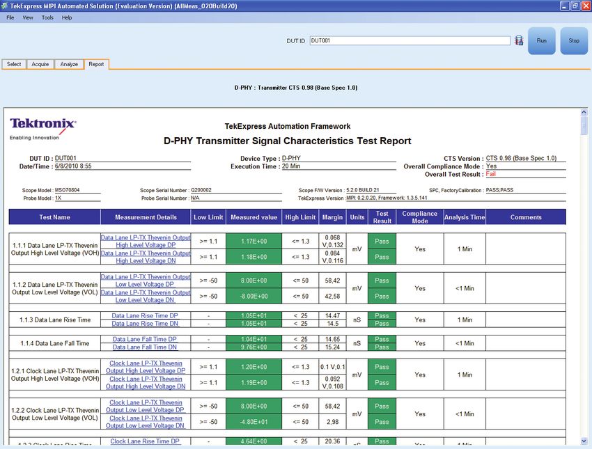
Understanding and Performing MIPI® D-PHY Physical Layer, CSI and DSI Protocol Layer Testing

                                                                    DSI or CSI-2 Protocol Testing Complexity
                                                                    DSI can be organized into several functional layers. The
                                                                    Physical layer is responsible for carrying the information
                                                                    between the Application processor and the peripheral (in this
                                                                    case the Display). The Physical layer conforms to the D-PHY
                                                                    specification.
                                                                    Lane Management Layer: The transmitter distributes the
                                                                    data that is transferred to several lanes (1 to 4) based on
                                                                    the bandwidth requirement.
                                                                    The protocol layer defines how the bits and bytes are
                                                                    organized into packets and which bits constitute the header
                                                                    and payload as well as taking care of the error checking.
                                                                    The application layer is responsible for interpreting the data
                                                                    from the below layer into pixel information or commands.
Figure 12. MIPI DSI Layered Architecture.

Planning for future capability & M-PHY
Planned for later implementation is a higher speed variant
of D-PHY called M-PHY. With data rates exceeding 5 Gb/s,
the M-PHY provides designers with the ability to speed up
memory transfer and CSI/DSI interface speeds.
The MIPI Alliance intends to have M-PHY be an extension to
existing D-PHY so that ongoing support for both PHY types
are expected in the future.
For testing considerations; M-PHY is an 8b/10b signal with
an embedded clock. It will require a faster oscilloscope for
the higher speed characterization efforts. In addition, M-PHY
signal integrity testing will need to include accurate clock
recovery methods like those found in the Tektronix DPOJET
platform. Look for more information as the M-PHY Testing
Specifications are completed in late 2010. In the interim,
contact Tektronix directly for more information and
planning support.

                                                                                                             www.tektronix.com/mipi   9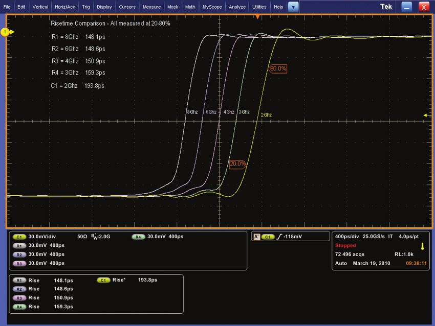
Application Note

Figure 13. Original Image.                                        Figure 14. Image Displayed on the Screen.

Figure 15. Typical Setup for DSI Digital Debug.

A mobile handset will consist of several subsystems. In most
cases each subsystem is developed separately and then all
the subsystems are integrated to make a complete system.
Consider a scenario when during system level integration
and testing the image in Figure 13 is sent by the applications
processor to the display.
In such scenario, the resulting image on the dispaly unit would
be as shown in Figure 14.
Figure 15 shows a typical setup that is used to debug this
                                                                  Figure 16. Listing Display.
problem. The D-PHY to P6980 adapter from The Moving Pixel
Company is a solder-in adapter that provides a single set of
loads to the system. It separates the LP and the HS signals
                                                                  when the links moves from LP mode to HS mode (and all the
before they are sent to the Logic Analyzer.
                                                                  states in between) before it begins to transmit highspeed DSI
The data that is acquired in the Logic Analyzer can be viewed     packets with image data. This provides link level information
at different levels of abstraction. The listing window shows      and helps in debugging the physical layer.
the state transitions that occur in the D-PHY Physical layer,

10   www.tektronix.com/mipi
Understanding and Performing MIPI® D-PHY Physical Layer, CSI and DSI Protocol Layer Testing
Figure 17. Protocol Decode Display.
Figure 18. Export Options.
Apart from this, the acquired data can also be exported and
saved as an image file; the image file can then be compared
with the display to verify the correctness. In the scenario that
we are considering, the image appears with a bluish tinge as
shown in Figure 19.
During the image export, options are provided to interchange
the RGB values as shown in the picture in Figure 18. These
options could be used to see if after interchanging the RGB
values the exported image matches the actual image that
is sent. Using these options we can figure out if the data is
Figure 19. Saved Image with Modified RGB values.
being sent incorrectly by the transmitter. Figure 19 shows the
exported image after the RGB values were interchanged.
The data can also be viewed at higher level of abstraction in
the protocol view. In this view the acquired data is decoded
into DSI packets and each field in the packet is decoded and
displayed and errors in the packet field or the ECC/Check-
sum are highlighted in red thus making it easy to identify any
transmission errors.
www.tektronix.com/mipi 11Application Note
If it turns out that the exported image matched the image
that was sent then it could be problem with the display. More
rigorous testing on the display can be done in a standalone
mode. The DSI decode SW also has the following features:
Decode and display of all types of Short and Long packets
of MIPI DSI
Supports all the following RGB Schemes:
- RGB-888
- RGB-565
- RGB-666 Packed Figure 20. Typical Setup for Display Testing.
- RGB-666 Loosely Packed
Supports upto 4 lanes To test the display subsystem separately the following
setup can be used. This setup can also be used during the
Image rendering capability. Stores the pixel information in
development of the display subsystem or to evaluate the
bmp format. Images are stored in C:\My Documents folder
performance of different displays without the need to integrate
Image rendering capability for DCS Command Support them into a full system. This involves using The Moving Pixel
Supports ECC and Checksum verification. If there is a PG3A with P331 D-PHY probe as a stimulus to generate the
mismatch, the Protocol Window displays the Error Packet DSI data over D-PHY. The P331 probe features four data lanes
in red and one clock lane. Data rate operation up to 1 Gb/s per lane
is supported. LP Voh, HS Voh and Vol are adjustable.
Provides an RGB Option to support different R, G and B
combinations The P331 also features an optional clock-in; the user can
supply a clock signal which will be then used as output clock
MIPI DSI Packet Summary feature is added. The Packet
signal as well as clock the data out in the HS mode. They can
Summary is written to a text file PktSummary.txt which is
also use this input to add jitter to the clock signal.
placed under “C:\My Documents”
Because of the flexibility of the P331, it is allows the user to
Renders partial images
test corner cases and recreate infrequent events to see the
Supports LPDT mode decoding system’s response to such events.
12 www.tektronix.com/mipiUnderstanding and Performing MIPI® D-PHY Physical Layer, CSI and DSI Protocol Layer Testing
In this way image or video information with several types of
commands can be sent to the display to verify the correctness
of the operation as well as compatibility with the other
subsystems. The variable voltage, timing and skew parameters
also allow us to do margin testing or evaluate display from
different vendors.
Apart from this the PG along with the P331 can also support
One lane to Four Lanes of D-PHY data
Support Data rates of upto 1 Gb/s
Supports both CSI2 and DSI protocols
Several parameters like the voltage, skew and the timing
can be varied on a per channel basis on both the High
Speed and the Low Power Modes.
The PG can play looping video and can insert commands
during active video.
The PG can be operated in several modes
Figure 21. PGRemote Software.
- Pushbutton Mode using the PGRemote software
The P331 probe is designed to be used with the PG-Remote - Macro Mode using the PGRemote software
software. The PG-Remote software is a separate software - Scripting
package that was expressly developed to provide an easy-
- Full remote control mode
to-use push button interface for user to generate the DSI
or the CSI2 data. The software allows the user to operate The PG can also be used as a general purpose instrument to
at a protocol level than at bit level. All the packet types and generate the required stimulus with different PG probes. The
the fields are predefined in the software the user must pick investment on a PG is preserved as it can be modified to
the packet type that needs to be generated and fill in the suit different applications by changing the probe to generate
packet fields and click the Send button. The PG takes care of different kinds of data.
formatting the data and generating the output that confirms
to the D-PHY standard. It also provides the option of creating
macros with a predefined set of commands and assigning it to
the button like other commands.
Once the setup shown in Figure 20 is done, an Image can
be sent to the display in a specific format preceded by all the
required commands to setup the display. This information
can also be acquired by the Logic Analyzer (optional). The
displayed image can then be compared to the image sent to
verify the correctness.
www.tektronix.com/mipi 13Summary Contact Tektronix:
ASEAN / Australasia (65) 6356 3900
The emergence of MIPI technologies solves a number Austria* 00800 2255 4835
of problems for the mobile industry around the need to Balkans, Israel, South Africa and other ISE Countries +41 52 675 3777
expand feature sets and improve battery life while increasing Belgium* 00800 2255 4835
Brazil +55 (11) 3759 7600
bandwidth and lowering costs through component reuse.
Canada 1 (800) 833-9200
The MIPI testing requirements involve a daunting set of PHY
Central East Europe, Ukraine and the Baltics +41 52 675 3777
layer checkpoints. The automated functionality provided by Central Europe & Greece +41 52 675 3777
TekExpress with Option D-PHYTX together with Tektronix Denmark +45 80 88 1401
oscilloscopes and probes shortens the time to market and Finland +41 52 675 3777
simplifies testing setup for D-PHY characterization and France* 00800 2255 4835
conformance tests to the latest specifications. Germany* 00800 2255 4835
Hong Kong 400-820-5835
India 000-800-650-1835
Italy* 00800 2255 4835
Japan 81 (3) 6714-3010
Luxembourg +41 52 675 3777
Mexico, Central/South America & Caribbean 52 (55) 56 04 50 90
Middle East, Asia and North Africa +41 52 675 3777
The Netherlands* 00800 2255 4835
Norway 800 16098
People’s Republic of China 400-820-5835
Poland +41 52 675 3777
Portugal 80 08 12370
Republic of Korea 001-800-8255-2835
Russia & CIS +7 (495) 7484900
South Africa +27 11 206 8360
Spain* 00800 2255 4835
Sweden* 00800 2255 4835
Switzerland* 00800 2255 4835
Taiwan 886 (2) 2722-9622
United Kingdom & Ireland* 00800 2255 4835
USA 1 (800) 833-9200
* If the European phone number above is not accessible,
please call +41 52 675 3777
Contact List Updated 25 May 2010
For Further Information
Tektronix maintains a comprehensive, constantly expanding collection of
application notes, technical briefs and other resources to help engineers
working on the cutting edge of technology. Please visit www.tektronix.com
Copyright © 2010, Tektronix. All rights reserved. Tektronix products are
covered by U.S. and foreign patents, issued and pending. Information in this
publication supersedes that in all previously published material. Specification
and price change privileges reserved. TEKTRONIX and TEK are registered
trademarks of Tektronix, Inc. All other trade names referenced are the service
marks, trademarks or registered trademarks of their respective companies.
09/10 EA/WWW 61W-25772-0You can also read