An efficient channelization architecture and its implementation for radio astronomy
←
→
Page content transcription
If your browser does not render page correctly, please read the page content below
Journal of Instrumentation

PAPER • OPEN ACCESS

An efficient channelization architecture and its implementation for radio
astronomy
To cite this article: W. Liu et al 2021 JINST 16 P08047

View the article online for updates and enhancements.

 This content was downloaded from IP address 46.4.80.155 on 08/10/2021 at 05:30
Published by IOP Publishing for Sissa Medialab
 Received: July 4, 2021
 Accepted: July 19, 2021
 Published: August 16, 2021

An efficient channelization architecture and its

 2021 JINST 16 P08047
implementation for radio astronomy

W. Liu, Q. Meng, ,∗ C. Wang, C. Zhou, S. Yao and I. Tariq
 Schoolof Information Science and Engineering, Southeast University,
 Nanjing, Jiangsu, China
 National Astronomical Observatories, Chinese Academy of Sciences,

 Beijing 100012, China

 E-mail: mengqiao@seu.edu.cn

Abstract: Channelization is one of the most important parts in a Digital Back-End(DBE) for
radio astronomy. A DBE with wider bandwidth and higher resolution consumes larger amount
of computing and memory resources, which results in much higher hardware cost. This paper
presents an efficient channelization architecture, which consists of Bit-Inverted, Parallel Complex
Fast Fourier Transform(BIPC-FFT) and In-place Forward-Backward Decomposition(IPFBD). The
efficient architecture can assist with saving a lot of resources, so a wide-band and high-resolution
DBE can be implemented on an resource restricted platform. Based on the efficient channelization
architecture, we designed a Dual-Input, 64K-Channelized prototype DBE with 1.2 GHz bandwidth
on a Xilinx Virtex-6 LX240T Field Programmable Gate Array(FPGA) chip. The test results in
the lab and observation results at Yunnan Observatory demonstrate the DBE can be used for radio
astronomy.

Keywords: Instrument optimisation; Spectrometers

 ∗ Corresponding author.

 c 2021 The Author(s). Published by IOP Publishing Ltd on behalf of
 Sissa Medialab. Original content from this work may be used under the
terms of the Creative Commons Attribution 4.0 licence. Any further distribution of this https://doi.org/10.1088/1748-0221/16/08/P08047
work must maintain attribution to the author(s) and the title of the work, journal citation
and DOI.
Contents

1 Introduction 1

2 Efficient channelization architecture and Its 64k-channelized implementation 2
 2.1 Hardware platform 3
 2.2 Efficient channelization architecture and implementation 4
 2.2.1 Bit-inverted, parallel complex FFT(BIPC-FFT) 4

 2021 JINST 16 P08047
 2.2.2 In-Place Forward-Backward Decomposition (IPFBD) 7
 2.2.3 Total resource consumption for the digital back-end 11

3 Results 11
 3.1 Test in the lab 11
 3.2 Observation at Yunnan Observatory 12

4 Conclusion 13

1 Introduction

Digital Back-End with wide bandwidth and high resolution is vital in radio astronomy, such as pulsar
observation and spectral line studies. Because of the significant distance among pulsars and earth,
the received pulsar signal is weak, so the receivers and digital back-end should have high sensitivity
for the weak signal, which makes the processing bandwidth get wider. For example, the bandwidth
of the ATA(Allen Telescope Array) is 209 MHz [1]. The bandwidth of the HartRAO is 400 MHz [2].
The bandwidth of the SKA(Square Kilometer Array) is up to 1 GHz [3] The bandwidth of the Parkes
is 2.8 GHz [4]. The bandwidth of EHT(Event Horizon Telescope) has reached to 4 GHz [5].
 Spectral line studies are operated at sky frequencies of Gigahertz to Terahertz, so the wide
processing bandwidth is also necessary. GREAT(German REceiver for Astronomy at Terahertz
frequencies) is a modular dual-color heterodyne instrument for highresolution far-infrared (FIR)
spectroscopy [6], and the IF bandwidth is up to 2.5 GHz. The new APEX(Atacama Pathfinder
EXperiment) telescope operates from several 100 GHz up to 1.5 THz, which allows for studies of
broader lines even at the highest frequencies [7].
 Spectral resolution has a large impact on the pulsar observation or spectral line studies. Because
of the impact of interstellar medium, the various frequencies of wide band pulsar signals coming to
the earth have distinctive time delays, which is called dispersion. High spectral resolution is helpful
in removing the dispersion effect, which is called incoherent dedispersion [8]. Higher resolution is
always required in spectral line research, therefore processing bandwidth up to several GHz with a
few thousand spectral channels is required, capable of resolving narrower spectral lines. [9–11].
 The approach to accomplish higher spectral resolution is to utilize larger number of spectral
channels. The Berkley-Parkes- Swinburne Recorder(BPSR) system developed based on Berkeley

 –1–

Table 1. Frequency channels of some famous digital back-end.

 Platform FPGA Model Number in BW(MHz) Freq ℎ Freq (kHz)
 SARDARA Xilinx Virtex6 SX475T 2 2500 16384 152.5
 XFFTS Xilinx Virtex6 LX 240T 1 2500 32768 76.2
 GUPPI Xilinx Virtex-II Pro 2VP50 2 1000 4096 244.1
 PDFB Virtex-4 SX55 2×2 1000 8192 122
 BPSR Xilinx Virtex-II Pro 2VP50 2 400 1024 390.6

CASPER’s IBOB has a maximum channel number of 1024 [12]. The Green Bank Ultimate Pulsar

 2021 JINST 16 P08047
Processing Instrument(GUPPI) system based on Berkeley CASPER’s IBOB has a maximum channel
number of 4096 [13]. The Pulsar Digital Filter Bank (PDFB) developed by Australia’s CISRO has
a maximum channel number of 8192 [14]. The eXtended bandwidth FFT Spectrometer(XFFTS)
system developed by Max Planck Lab in Germany is based on a Xilinx Virtex-6 LX240T FPGA chip,
and the maximum number of frequency channels is 32768 [9]. Another approach is to finish coarsely
channelization in FPGA, and then acquire higher spectral resolution in subsequent processing. For
example, rather than attempting to achieve the desired channel resolution by performing a larger
FFT on FPGA, the SArdinia Roach2-based Digital Architecture for Radio Astronomy(SARDARA)
based on the ROACH21 platform uses a Xilinx Virtex-6 SX475T FPGA as the signal processing
core, dividing the broadband signal into 16384 frequency channels [15]. This data is then sent over
ethernet to a GPU server, which performs the subsequent fine channel splitting. [16–18]. With the
incredible processing capacity of GPU, the number of spectral channels can reach to million, but
GPU increases equipment cost and power consumption. Bandwidth and spectral channels of the
digital back-ends are shown in table 1.
 The key of channelization processing is to perform FFT on the digitized input signal. However,
the hardware resource, especially the Block RAM(BRAM) resources, on FPGA chip limits the
number of spectral channels. Among the digital back-ends seen so far, Xilinx Virtex-6 SX 475T
FPGA on ROACH2 platform has the most hardware resource, especially the largest amount of
BRAM resources at 38,304 Kb, and the maximum number of channels supported by it is 16384
for dual-input analog input signals. XFFTS is another powerful spectrometer with the maximum
number of spectral channels up to 32768. Currently, many FPGA chips have more hardware
resources, which can be used for larger amount of spectral channels, but the powerful FPGA chips
result in higher hardware costs.
 In this paper, an efficient channelization architecture is present, which can help to acquire more
spectral channels with limited hardware resources. With the efficient architecture, a dual-input,
64K-Channelized prototype digital back-end is implemented on a Xilinx Virtex-6 LX240T FPGA
chip with the spectral resolution of 18.3 kHz in 1.2 GHz bandwidth.

2 Efficient channelization architecture and Its 64k-channelized implementation

Table 1 shows that the majority of digital back-ends are built for dual analog inputs. The reason for
this is that signals received by the antenna are usually split into right-polarized and left-polarized
 1https://github.com/casper-astro/casper-hardware.

 –2–
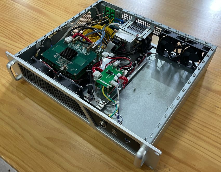
input components, and these two input components are occasionally required for radio astronomy
research, such as the determination of Stokes parameters in pulsar observation. In this way, the
digital back-end should be able to process these two signals simultaneously.

2.1 Hardware platform

The digital back-end implemented in this paper is based on our Cascaded Reconfigurable Architec-
ture Board(CRABoard) [19], which consists of three parts. The first part is ADC(Analog-to-Digital
Converter) sampling board based on EV8AQ160, capable of dual-channel input with 2.4 GSps sam-
pling rate and 8-bit resolution. The second is an FPGA signal processing board based on a Xilinx

 2021 JINST 16 P08047
Virtex-6 LX240T FPGA chip. The last is an ARM-based control board, which can be utilized for
initialization and control. The system block diagram is shown in figure 1. The photo of the digital
back-end is shown in figure 2.

 Figure 1. Block diagram of the Digital Back-End system.

 CASPER toolflow2 is world famous, and it allows researches to generate signal processing
designs using MATLAB’s graphical programming tool Simulink. At the beginning of the design,
we tried CASPER toolflow(for ROACH2) to implement some spectrometer designs, which can be
used for the estimation of resource consumption, which is shown in table 2.

 Table 2. The resource consumption for different spectral channels(one input channel).

 Slice Logic
 Occupied Slices LUT Flip Flop pairs used RAMB18E1
 Channels
 16384 7837 27485 535
 32768 9806 33706 1071
 65536 - - Exceeded

 2https://casper-toolflow.readthedocs.io/en/latest/.

 –3–
2021 JINST 16 P08047
 Figure 2. The photo of the Digital Back-End.

 From the table, we can see the resources are not enough for a one-input, 64K-Channelized
design on ROACH2, so the resources must also be exceeded on our hardware platform, which is
based on a Xilinx Virtex-6 LX240T chip. The channelization implementation consumes most of
the resources, so we have to utilize an more efficient channelization architecture.

2.2 Efficient channelization architecture and implementation

The signal processing diagram of the entire digital back-end is shown in figure 3, which is consisted
of five units: Data Interface Unit, Power Calculating Unit, Accumulation Unit, Ethernet Unit and
64K-Channelized Unit for Dual Input Channels. As the analog input signals, and , are sampled
at 2.4 GSps, it is hard to process the high-speed data stream directly. The data interface unite is
used to divide the data stream into eight separate data streams at 300 MSps. The Power Calculation
Unit is used to calculate the input power of the signals. The Accumulation Unit is used for power
accumulation. The Ethernet Unit is used for transferring raw channelized data from FPGA. The
64-Channelized Unit is based on the efficient channelization architecture, which is the core in the
whole system. The efficient channelization architecture is shown in figure 4, and we will introduce
the key parts in the efficient architecture in section 2.2.1 and section 2.2.2.

2.2.1 Bit-inverted, parallel complex FFT(BIPC-FFT)
As previously stated, the digital back-end should process both left- and right-polarized input signals
at the same time. Two separate FFT modules are used in the traditional technique. The input data
is only assigned to the real part of the FFT input since the input signal is a real signal. When we
try to execute 64K channelization, this method takes a lot of BRAM resources, which the FPGA
cannot provide. We propose Bit-Inverted, Parallel Complex FFT, which treats left-polarized and
right-polarized signals as the real and imaginary components of a complex signal to save hardware
resources. Following the completion of the FFT process, a decomposition module is used to decom-
pose the FFT output into the real and imaginary parts of the FFT input, which correspond to left-

 –4–
2021 JINST 16 P08047 Figure 3. Signal processing diagram of the 64K-Channelized digital back-end. Figure 4. The 64K-Channelized module based on the efficient channelization architecture. polarized and right-polarized signals. By utilizing the complex FFT, only a single FFT module is ex- pected to complete the 64K channelization, and it saves half of the resources required by FFT module. Suppose ( ) and ( ) are N-point real data streams, which corresponding to the right- polarized and left-polarized data, and ( ) and ( ) are their DFT: ( ) = DFT[ ( )], ( ) = DFT( ( )) Let ( ) = ( ) + ∗ ( ) (2.1) Then the DFT will be ( ) = DFT( ( )) = DFT( ( )) + ∗ DFT( ( )) (2.2) = ( ) + ∗ ( ) Due to the conjugate symmetry of ( ) and ( ), we will get 1 ∗ ( ) = 2 ( ( ) + ( − )) (2.3) ( ) = − ( ( ) − ∗ ( − )) 2 Therefore, ( ) and ( ) can be calculated with only one FFT module [20]. Because the data stream has to be processed in real time, a Pipelined FFT IP core that can process the data as a stream must be implemented. However, because the sampling rate of the and in this architecture is 2.4 GSps, the FPGA clock rate would exceed the fabric capability –5–
2021 JINST 16 P08047
 Figure 5. Block diagram of the PC-FFT

if processed as a single data stream on the FPGA. The high-speed data stream must be divided
into several parallel data streams and then input to the logic part of FPGA. As the high-speed data
stream has been divided into eight sub data streams by the data interface unit, the eight parallel
data streams are perfect to the 64K-Channelized unit. To finish the Real-Time, High-Speed FFT
computation, a parallel processing method must be applied. The block diagram of BIPC-FFT is
shown in figure 5. Eight pipeline FFT cores are used to perform eight 16K-Point FFT in parallel,
and then one Radix-2 FFT module and two Radix-4 FFT modules are implemented to finish the
whole FFT computation [19, 21, 22].
 In figure 5, the twiddle factor is needed for FFT butterfly, which is generally a set of sin/cos
data tables stored in BRAM. As the number of FFT points increases, the BRAM consumption
also increases accordingly. In order to save BRAM resources, the CORDIC (Coordinate Rotation
Digital Computer) core, which is based on a digital calculation algorithm of coordinate rotation,is
utilized to generate the twiddle factor and reducing consumption of BRAM resource.
 In the realization of 16K-Point Pipelined FFT module in figure 5, there are two kinds of Xilinx
FFT IP cores in Xilinx ISE. One works on sequential mode, and another works on Bit-Inverted mode.
The BRAM consumption under each IP core is shown in the table 3. The selection of the FFT IP
core will also affect the design of the decomposition module in figure 4. When a sequential FFT IP
core is selected, the realization of the decomposition will be easier, but FFT core consumes a large
amount of BRAM. If a Bit-Inverted FFT IP core is selected, the amount of BRAM resources will be
decreased, but the decomposition will be more complex due to the inverted order of the data. Virtex-
6 LX240T FPGA only has a total of 832 18 Kb-BRAM blocks. In order to save the BRAM resources,
the Bit-Inverted FFT IP core is utilized. However, the difficulties in decomposition process under
Bit-Inverted mode must be carefully resolved, which will be discussed in Session 2.2.2.

 –6–
Table 3. BRAM consumption for FFT (the input data width is 8 bits).

 18 Kb BRAM Consumption
 16K Pipeline FFT with Sequential output 68 × 8
 16K Pipeline FFT with Bit-Inverted output 27 × 8

 2021 JINST 16 P08047
 (a) Sequential Order Mode

 (b) Bit-Inverted Order Mode

 Figure 6. The order of 8-Channel output data of FFT module

2.2.2 In-Place Forward-Backward Decomposition (IPFBD)

In the design of the decomposition part, the Bit-Inverted order of the input data from the FFT module
must be processed first. Taking 32-point FFT as an example, the input data is divided into eight
streams at 300 MSps for eight sub FFT calculation, and the output order of sequential FFT output
and Bit-Inverted FFT output are shown in figure 6(a) and figure 6(b) respectively. In Bit-Inverted
order mode, there are eight output data streams: SUB_FFT_STREAM0∼SUB_FFT_STREAM7.

 –7–
2021 JINST 16 P08047
 Figure 7. upper/lower streams and the pairing method.

In the th stream at , the corresponding index of ( ) will be:

 = × + BitInvert( , )
 8 (2.4)

 = , = 0 ∼ 7, = 0 ∼ − 1
 8
Where BitInvert( , ) refers to a M-bit Bit-Inverted function to q. Because the ( ) and ( )
are real signals, we only need to calculate the first half of ( ) and ( ), where = 0 ∼ ( 2 − 1).
 From equation (2.3), we can see that in order to calculate ( ) and ( ) in a given , only
a pair of data is needed: ( ) and ( − ). Therefore, we can split the streams in figure 6(b) into
two groups: SUB_FFT_STREAM0∼3 refer to the upper-streams and SUB_FFT_STREAM4∼7
refer to the lower-streams.
 The upper/lower streams and the pairing method is shown in figure 7. There are two things we
can find from figure 7. The first is that for a given (0 ∼ 2 − 1), ( ) and ( − ) appear in
the upper-streams and lower-streams respectively. The second thing is that the required ( ) and
 ( − ) sometimes appear at the same time, but sometimes not. For example, in order to calculate
 (2) and (2), we need (2) and (30), which both appear in 2. However, for calculating
 (1) and (1), we need (1) and (31), which appear at 2 and 3 respectively. Since the
PC-FFT module is a Real-Time arithmetic module, a buffer is necessary to catch data between the
output of PC-FFT and the input of the decomposition module.
 Traditionally, a Ping-Pong buffering method could be used in these situations. It consists of
two identical buffers. At a time, one buffer is used for caching current data, and another buffer,
which contains the previous data of streams, is used as the input of the decomposition module. It is
relatively simple, but the disadvantage is that it requires more BRAM for the buffer. In this design,
256 18Kb-BRAM blocks are needed for the Ping-Pong buffer storage of data stream(18bit data
width), which is a large consumption of BRAM resource. Therefore, an In-Place buffering method
with one buffer is required.
 IPFBD method is implemented for saving BRAM resources. When decomposing ( ) and
 ( ), ( ) and ( − ) will be read out from the buffer. New output data from PC-FFT module

 –8–
can be written to the same address to take the place for ( ) and ( − ) in the same buffer at the
same time. Therefore, only one buffer is required in IPFBD. Comparing to the Ping-Pong buffering
method, half of the buffer resource is saved.
 Also taking 32-point FFT as an example. Suppose in the previous step, the ( ) is stored in
the buffer as the same order shown in figure 6(b), and the storage map is illustrated in figure 8(a),
which is at the time, 0. Then the first round of decomposition happens like this:

(1) In the first step, 1, the first column of the streams is used to decompose ( ), ( )
 where = 0, 4, 8, 12. According to equation (2.3), (0), (4), (8), (12), (16), (20),
 (24), (28) are required. After the decomposition, new data can be written to the first row,

 2021 JINST 16 P08047
 as figure 8(b).

(2) In the second step, 2, the second column is processed in the similar way as what happened
 at 1, which is illustrated in figure 8(c).

(3) In the third step, 3, things happened differently. The required data of the upper-streams
 exists in the third column, but for the lower streams it exists in the fourth column. Therefore, the
 new data must be written to the third and fourth column respectively, as shown in figure 8(d).

(4) In the fourth step, 4, the fourth column in the upper streams is processed in the similar way
 as step 3, which is illustrated in figure 8(e). This is the end of decomposition of this round, and
 new data was written to the buffer.

 From above procedure, we can see that the column address of the lower-streams is little more
complex. Sometimes it goes forward, sometimes backward. It can be calculated according to
equation (2.3)and (2.4).
 After the first round of the decomposition, the storage of the ( ) is illustrated in figure 8(e).
By studying the arrangement of the ( ) in this time, we can find out that all the necessary data
of the upper-streams and lower-streams happens to be in the same columns. It will be good news
for the next round decomposition, for the read/write order of the column address could be all in
forward mode at this time. Therefore, after the second round decomposition, the new ( ) will be
arranged as figure 8(f), which is in a similar order as figure 8(a). And then the next third round of
decomposition will be the same as the first round.
 There are two kind of addressing modes for the lower-streams in the decomposition procedure:
the first is described above, known as the first round decomposition; the second is sequential. These
two kinds of addressing mode are used alternatively in the whole time to construct an In-Place
buffering algorithm.
 In Xilinx ISE, the True Dual-Port RAM(TDP-RAM) works on Read-First can be used for the
In-Place method. In Read-First mode,3 data previously stored at the Write address shows up on the
data output port, while the input data is being stored in the memory [23]. Therefore, the IPFBD
algorithm can be implemented for pipeline decomposition with only one TDP-RAM, which can save
half of the BRAM resources. Comparison between the two buffering methods is shown in table 4.
 In summary, The total 18Kb BRAM consumption for the 64K-Channlized core is 344 18 Kb-
BRAM blocks, which is 41.3% of total 18Kb-BRAM on Xilinx Virtex-6 LX240T FPGA chip.
 3https://www.xilinx.com/support/documentation/ip_documentation/blk_mem_gen/v7_3/pg058-blk-mem-gen.pdf.

 –9–
2021 JINST 16 P08047
Figure 8. Data steam updating in the buffer. ( ) means the ( ) in the th round of calculation.

 Table 4. BRAM consumption for Ping-Pong Method and IPFBD(The output bit width is 18 bits.)

 18 Kb BRAM Consumption
 Ping-Pong Method 16 × 8×2
 IPFBD Algorithm 16 × 8

 – 10 –
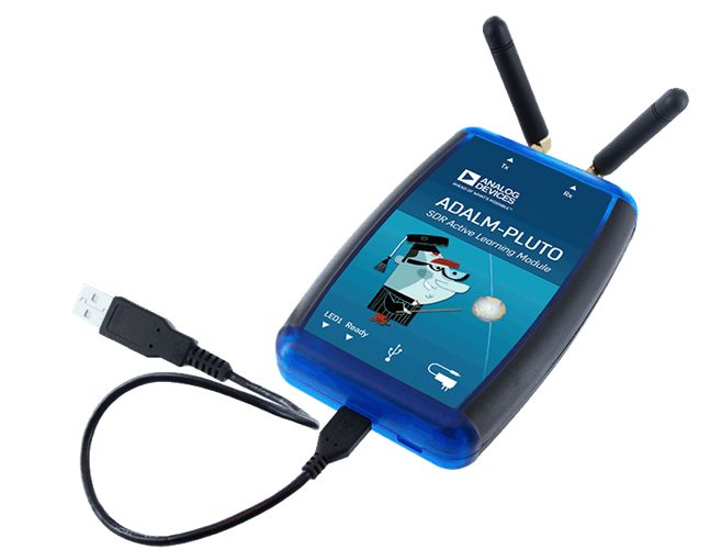
Table 5. Summary of BRAM consumption for the 64K-Channelized core.

 18 Kb BRAM Consumption
 PC-FFT 27 × 8
 IPFBD 16 × 8
 Total 344

2.2.3 Total resource consumption for the digital back-end
With PC-FFT and IPFBD, we implemented a DGB. It consists all necessary modules, such as ADC-

 2021 JINST 16 P08047
input, Dual-Input 64K-Channelized, power accumulation, Ethernet and state monitoring module
and etc. The total resources consumption is illustrated in table 6. The total BRAM consumption
is 96% on Xilinx Virtex-6 LX240T. Therefore, we can see that the reduced BRAM usage due to
the new methodology allows for a doubling of the spectral resolution. Without these changes, the
usage at this resolution would have exceeded the FPGA resources.

 Table 6. Total Resource Consumption.

 Slice Logic Utilization Used Utilization
 Number of Occupied Slices 18250 48%
 Number of LUT Flip Flop pairs used 60209 20%
 Number of RAMB18E1 768 92%

3 Results

With the efficient channelization architecture, we implemented a 64K-Channelized digital back-
end with high frequency resolution (18.3 kHz) and wide bandwidth (1.2 GHz) based on Virtex-6
LX240T FPGA. We did the test in the laboratory to confirm the high frequency resolution, and the
we took the backend to Yunnan Observatory for the pulsar observation experiment.

3.1 Test in the lab

In the 64K-Channelized digital back-end, the frequency resolution is 18.3 kHz, so we can gen-
erate a two-tone signal with two Δ frequency difference. An ADALM-PLUTO4 from ADI
(Analog Devices) was used as the signal generator, which can generate the two-tone signal. The
photo of ADALM-PLUTO is shown in figure 9. The two frequencies we suppose to have are
453.22265625 MHz and 453.25927734 MHz.
 With the digital back-end, we can get the frequency spectra data from the Ethernet port on the
back-end, and the result is shown in figure 10. The test result demonstrates that the 64K-Channelized
digital back-end has high spectral resolution and it can be implemented on a resource-limited FPGA
chip, such as a Xilinx Virtex-6 LX240T FPGA chip.

 4https://www.analog.com/en/design-center/evaluation-hardware-and-software/evaluation-boards-kits/adalm-
pluto.html.

 – 11 –
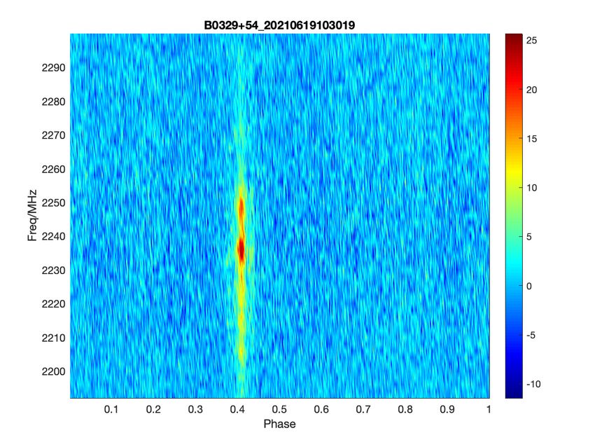
2021 JINST 16 P08047
 Figure 9. The photo of ADALM-PLUTO.

 Figure 10. Power spectra of the two-tone signal.

3.2 Observation at Yunnan Observatory

We also did pulsar observation experiment successfully at Yunnan Observatory on June 18, 2021
with the digital back-end. The pulsar we observed is B0329+54. The some of the information about
the pulsar is shown in table 7, which is from the ATNF5 pulsar database [24].
 The observation is completed on S-band. The S-band receiver at Yunnan Observatory covers
from 2190 MHz to 2300 MHz, and the frequency of LO(Local Oscillator) is 2000 MHz, so the valid
IF(intermediate frequency) is from 190 MHz to 300 MHz, which is shown in following figures.
 In the design, the number of frequency channels is 65536, and the frequency resolution is
18.3 kHz. We finished 5-minute observation at Yunnan Observatory. The period of B0329+54 is
about 0.714 s, and the period folded results are shown in figure 11. In the two figures, -axis refers
to phase, ranging from 0 to 1.

 5https://www.atnf.csiro.au/research/pulsar/psrcat/.

 – 12 –
Table 7. The information about B0329+54.

 Parameters Values
 NAME B0329+54
 DM 26.7641
 PEPOCH 46473.00
 P0 0.714519699726s
 P1 2.048265E-15s/s

 2021 JINST 16 P08047
 (a) (b)

 Figure 11. (a) The Phase-Frequency figure of B0329+54. (b) The profile of B0329+54.

 The frequency resolution of the digital back-end is 18.3 kHz, so the number of frequency
channels in the 110 MHz observed bandwidth is
 110 MHz
 =≈ 6011 (3.1)
 18.3 kHz
Therefore, the power of the pulsar is distributed among 6011 channels, which makes the signal not
clear in the Phase-Frequency figure. We added up the power of 110 consecutive spectral channels,
and obtained 55 equivalent spectral channels. The bandwidth of each equivalent spectral channel
is 11 MHz. The processed result is shown in figure 12.
 The comparing of figure 11(a) and figure 12 can also demonstrate that the digital back-end has
high frequency resolution.

4 Conclusion

An efficient channelization architecture, consisting of BIPC-FFT and IPBFD, is present in this paper.
The efficient architecture can assist save a significant amount of hardware resources, allowing a
wide-bandwidth and high-resolution digital back-end to be implemented on a hardware platform
with limited resources. With the efficient architecture, a Dual-Input, 64K-Channelized prototype
digital back-end with 18.3 kHz spectral resolution and 1.2 GHz bandwidth is implemented on a
Xilinx Virtex-6 LX240T FPGA chip, which makes full use of FPGA resources, improves resource

 – 13 –
2021 JINST 16 P08047
 Figure 12. The observing bandwith is divided into 55 spectral channels.

efficiency. It is possible to implement a more powerful digital back-end on a more advanced FPGA
chip with the efficient architecture.

Acknowledgments

This work was supported by The National Natural Science Foundation of China under Grant
U1731120. The authors also gratefully acknowledge the helpful comments and suggestions from
the reviewers. We also thank the staff of Yunnan Astronomical Observatory for their help.

References

 [1] A. P. Siemion, D. Werthimer, G. Marcy and M. W. Leeuwen, The fly’s eye: Instrumentation for
 detection of radio ephemeron, https://casper.berkeley.edu.
 [2] S. J. Bell Burnell, Little green men, white dwarfs or pulsars?, Cosmic Search 1 (1979) 16.
 [3] F. Combes, The Square Kilometer Array: cosmology, pulsars and other physics with the SKA,
 2015 JINST 10 C09001 [arXiv:1504.00493].
 [4] L. Levin et al., The High Time Resolution Universe Pulsar Survey VIII: The Galactic millisecond
 pulsar population, Mon. Not. Roy. Astron. Soc. 434 (2013) 1387 [arXiv:1306.4190].
 [5] J.P.W. Verbiest et al., Timing stability of millisecond pulsars and prospects for gravitational-wave
 detection, Mon. Not. Roy. Astron. Soc. 400 (2009) 951 [arXiv:0908.0244].
 [6] S. Heyminck, U.U. Graf, R. Gusten, J. Stutzki, H.W. Hubers and P. Hartogh, GREAT: the SOFIA
 high-frequency heterodyne instrument, Astron. Astrophys. 542 (2012) L1.
 [7] R. Güsten, L. Nyman, P. Schilke, K. Menten, C. Cesarsky and R. Booth, The atacama pathfinder
 experiment (apex)–a new submillimeter facility for southern skies–, Astron. Astrophys. 454 (2006)
 L13.
 [8] T.H. Hankins and B.J. Rickett, Pulsar signal processing, Meth. Comput. Phys. 14 (1975) 55.

 – 14 –
[9] B. Klein, S. Hochgurtel, I. Kramer, A. Bell, K. Meyer and R. Gusten, High-resolution wide-band Fast
 Fourier Transform spectrometers, Astron. Astrophys. 542 (2012) L3 [arXiv:1203.3972].
[10] S. Stanko, B. Klein and J. Kerp, A Field programmable gate array spectrometer for radio astronomy.
 First light at the Effelsberg 100-m telescope, Astron. Astrophys. 436 (2005) 391
 [astro-ph/0503067].
[11] B. Klein, S. D. Philipp, R. Güsten, I. Krämer and D. Samtleben, A new generation of spectrometers
 for radio astronomy: Fast fourier transform spectrometer, Proc. SPIE 6275 (2006) 627511.
[12] M.J. Keith et al., The High Time Resolution Universe Pulsar Survey I: System configuration and
 initial discoveries, Mon. Not. Roy. Astron. Soc. 409 (2010) 619 [arXiv:1006.5744].

 2021 JINST 16 P08047
[13] R. DuPlain, S. Ransom, P. Demorest, P. Brandt, J. Ford and A. L. Shelton, Launching guppi: the
 green bank ultimate pulsar processing instrument, Proc. SPIE 7019 (2008) 70191D.
[14] G. Hampson, A. Brown and C. Vimiera, A 1 GHz pulsar digital filter bank and RFI mitigation system,
 Australia Telescope National Facilty (2008).
[15] A. Melis, R. Concu, A. Trois, A. Possenti, A. Bocchinu, P. Bolli et al., Sardinia Roach2-based Digital
 Architecture for Radio Astronomy (SARDARA), J. Astron. Instrum. 7 (2018) 1850004.
[16] J. Kocz, L. Greenhill, B. Barsdell, D. Price, G. Bernardi, S. Bourke et al., Digital signal processing
 using stream high performance computing: a 512-input broadband correlator for radio astronomy,
 J. Astron. Instrum. 4 (2015) 1550003.
[17] MITEoR collaboration, MITEoR: a scalable interferometer for precision 21 cm cosmology, Mon. Not.
 Roy. Astron. Soc. 445 (2014) 1084 [arXiv:1405.5527].
[18] J. Zwart, R. Barker, P. Biddulph, D. Bly, R. Boysen, A. Brown et al., The Arcminute Microkelvin
 Imager, Mon. Not. Roy. Astron. Soc. 391 (2008) 1545 [arXiv:0807.2469].
[19] W. Liu, Q. Meng, J.-L. Han, C. Wang, T. Zhang and X. Dong, A 1.2 ghz bandwidth digital backend
 for pulsar observation, in proceedings of Progress in Electromagnetics Research Symposium-Fall,
 Singapore, 19–22 November 2017, pp. .
[20] H.J. Nussbaumer, The fast fourier transform, in Fast Fourier Transform and Convolution Algorithms,
 Springer (1981), pp. 80–111.
[21] D. Werthimer, The CASPER collaboration for high-performance open source digital radio astronomy
 instrumentation, in proceedings of the XXXth URSI general assembly and scientific symposium,
 Istanbul, Turkey, 13–20 August 2011, pp. 1–4.
[22] X. Wang, Q. Meng, H. Jinlin, W. Chen and J. Zhang, A wideband real-time spectrometer based on
 combined complex fft for radio astronomy, in proceedings of the 9th International Symposium on
 Communication Systems, Networks & Digital Sign, Manchester, U.K., 23–25 July 2014, pp. 685–689.
[23] Xilinx, LogiCORE IP, Block memory generator.
[24] R.N. Manchester, G.B. Hobbs, A. Teoh and M. Hobbs, The Australia Telescope National Facility
 pulsar catalogue, Astron. J. 129 (2005) 1993 [astro-ph/0412641].

 – 15 –
You can also read