Upgrade Phase 2 Overview - CERN Indico
←
→
Page content transcription
If your browser does not render page correctly, please read the page content below
Upgrade Phase 2 Overview
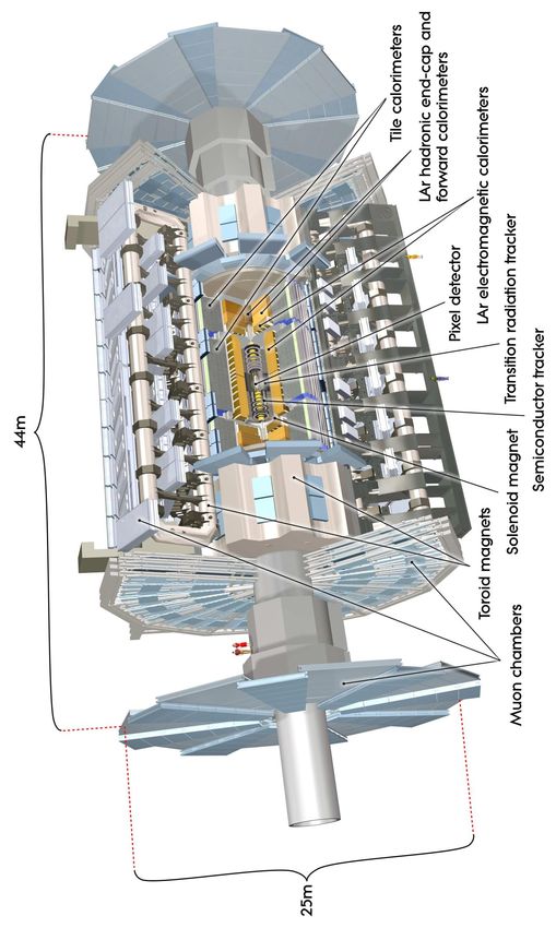
Introduction ATLAS detector will be upgraded to match with the increased luminosity at HL-LHC Overview in this talk only for Phase-2 Reminder of the HL-LHC key features: • Total luminosity of 3000 fb-1 at 14 TeV each for ATLAS and CMS (ultimate scenario is 4000 fb-1). • Baseline instantaneous luminosity of ℒ = 5 x 1034 cm-2 s-1 (ultimate achievable ℒ = 7.5 x 1034 cm-2 s-1). • Number of collisions per bunch crossing ⟨ ⟩~140 (ultimate scenario ⟨ ⟩~200). Installation completed in 2026 for commissioning towards early 2027 26-28 May 2020 D. Ferrere - ATLAS Upgrade Overview 2
HL Physics Program
 Physics benchmarks are investigated by Working Groups
 WG1: Standard Model [CERN LPCC-2018-03]
– Precision measurements (Weinberg angle, W and top masses, etc.)
– Rare signatures (four top, FCNC top decays, etc.)

 WG2: Higgs [CERN LPCC-2018-04]
– Properties: couplings and self coupling, precision mass and width measurements
– BSM Higgs searches, invisible decays

 WG3: Beyond Standard Model [CERN LPCC-2018-05]
– Prompt and long-lived particles signatures
– Supersymmetry, dark matter, resonant searches, etc.

 WG4: Flavour Physics [CERN LPCC-2018-06]
– CKM observables
– bottom, charm and strange probes for new Physics, LFV with taus
– B anomalies studies

 WG5: High Density QCD and Heavy Ions [CERN LPCC-2018-07]
– Studies with both heavy ions and proton beams
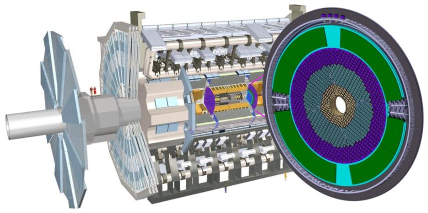
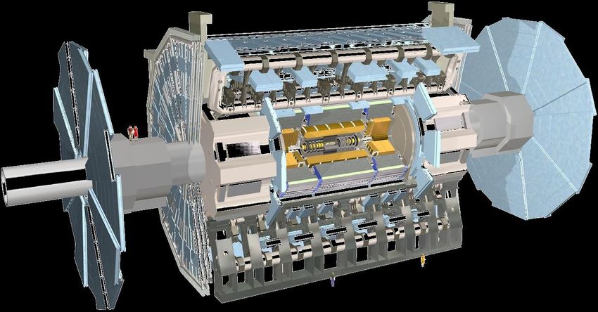
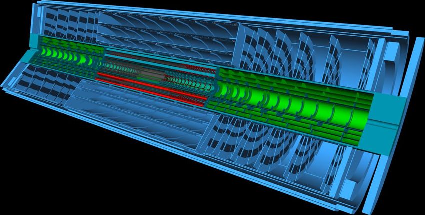
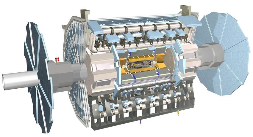
ATLAS Detector Phase-2 Upgrade Plan

 HGTD
 (under approval)

 ITk Pixel

 ITk
 ITk Strip
Goal and Challenge Goal at HL-LHC: • At least the same performance as in Run-2/Run-3 (tracking, b-tagging, ETmiss, …) • Trigger rate tuned for low pT threshold ( at least a factor 10 increase) • Extension of tracking coverage and pile-up mitigation up to large ( Run-1 20 ~0.04 @ 7 TeV HL-LHC 200 ~7.4 @ 14 TeV
Radiation Damage Active components are to sustain optimal performance up to 4000 fb-1 except for the ITk Pixel Inner System which will be replaced after 2000 fb-1. HGTD Innermost rings will also have to be replaced. Detector technologies (Si planar, 3D, LGAD and diamond) : ‐ NIEL bulk damage (trapping centers) leading to depletion voltage and leakage current increase Deep sub-micron technologies & FPGAs are to be qualified wrt : - TID surface effects, transistor damage and ageing effects - SEE (SEL, SET, SEU) which are induced effects by heavy ions and hadrons either soft errors (No permanent damage like SEU, SET,… ) or hard errors (permanent damage like SEL) Material (cable, glue, composite…) ‐ TID can compromise chemical/mechanical integrity Heavy and lengthy qualification process for all sub-systems

Further details will be presented by:
P. Phillips (ITk OT)
F. Huegging (ITk IT)
ITk Layout Tracking capability up to < 4 (Pixel) with increased granularity of up to x8 wrt the ID Surface [m2] # Channels # modules Pixel 13 (x7) 5.1 G (x60) 9.2 k Strip 165 (x3) 60 M (x10) 18 k Strip Endcap From 33mm up ~1m radius Strip Barrel Tracking extension coverage Pixel Outer Barrel (~50% 0f the surface) Pixel Inner System (IS) Pixel Outer Endcap will be replaced after 2000 fb-1

Material Budget
Design choice was motivated with minimization of the material budget
With the increased surface and granularity, X0 mitigation thanks to:
• Strip: DC-DC powering and data transmission with optical links and lpGBT
• Pixel: Thinned sensors and FE, Serial powering, inclined region in the Outer Barrel,
 readout bandwidth (x8 increase or 1.28 Gbps uplinks)
• Common (ITK and Stip): Light structures, cooling designs optimized as well as material
 choice wrt the requirements (precision, stability, contain the thermal run away, …)
NB: Material budget is regularly updated as the engineering design evolves
 Current ID ITk
 Not the latest version…
ITk Pixel Sensors • Sensor Quad modules of ~4x4 cm2 for L1 to L4 with 50x50 µm2 pixel size n-in-p planar sensor technology (bias up to 600V due to radiation effects) Market survey in finalization • Innermost layer (L0) with 25x100 µm2 for the barrel and 50x50 µm2 for rings 3D sensor technology (bias up to 250V at the end of life time) Recent decision to shift the radius from 39 mm to 33 mm (disks) - 34 mm (barrel) Test beam data for planar and 3D technology demonstrating that it is compliant even for the most demanding layers Additional results will be available by mid of 2021… CNM 150 µm + RD53A at 5x10¹⁵ 1 MeV neq/cm2 CNM 150 µm + RD53A at 1x10¹⁶ 1 MeV neq/cm2 25x100, 1E 25x100, 1E 26-28 May 2020
ITk Pixel Module RD53A Quad Module Module development tightly bound to the FE readout FEI4 RD53A ITkPixV1 Production (v1 or v2) now start ~2 years • ITkPixV1 just submitted (17.03.2020) and wafers expected ~mid-June. • V2 may add Regional Readout (RR) feature that can be used to read out modules inside a region of interest at a 4 MHz L0 trigger, while keeping the average readout rate comparable to the L1 trigger rate of ~1 MHz (connected to TDAQ) • Hybridization Market Survey progressing with RD53A while vendors are asked in parallel to make ITkPixV1 modules • Common module flex design is almost completed with pigtail interconnect • Module production with tooling and QC are being setup 26-28 May 2020
ITk Pixel Powering & Readout Up to 14 modules in a Serial Powering (SP) chain considered: - Module (voltage) regulation by an on-chip Shunt LDO - Voltage cascade with reference at PP0. Dedicated DCS chip for monitoring. - Module HV will be offset with local module reference (at least 2 channels/SP chain) Successfully tested with FEI4 and RD53A modules (See talk M. Hamer ) Module data links: - From 4 links per FE and down to ¼ link per FE (or 1 link / Quad) @ 1.28 Gbps each - 1 downlink for clock and command serving up to 3 modules @ 160 Mbps - GBCR is a specific chip development to equalize upstream links and transmit downlinks 160 Mbps Twinax up to 6 m 1.28 Gbps 26-28 May 2020
ITk Strip Overview Strip Endcap Strip Barrel Pixel Barrel: 4 barrel layers instrumented with modules on the two sides of the stave local support Endcap: 6 disks instrumented with modules on the two sides of the petal local support Barrel Endcap # of modules 10976 6912 # of Local Support 392 384 Surface [m2] 104.8 60.4 Endcap: Petal is loaded with 18 modules Length ~ 60cm Barrel: Stave is loaded with 28 modules Length ~ 140 cm 26-28 May 2020
ITk Strip Modules
 Module: sensor + hybrid + power board with wire bond interconnects
 Hybrid: Hosts ABCStar, HCCStar, AMAC02 + Power board with DC-
 DC converter and HV filter and switch
 Sensor types:
 • Barrel: Short and long strips EC R0 module
 • Endcap: R0 to R5 flavors
 Long strip module

 Short strip module
 Test beam results with irradiated modules

 ATLAS ITk Preliminary ATLAS ITk Preliminary Enough safety margin to be
 above 99% efficiency after end
 of detector life time in all layers
 (Ring-0, Long strip and short
 strip)

 Module now in pre-production

26-28 May 2020
ITk Strip Local Support Stave Module Loading Petal Module Loading Transition period from prototype fully loaded local support structure pre-production Very good progress achieved with fully working stave! 26-28 May 2020
Further details will be presented by:
 C. De La Taille
 F. Salomon

26-28 May 2020
LAr Upgrade Plan
 Main Goal of upgrade:
 • Replace the readout electronics to cope with the increased trigger rate and pile up
 • Improve the granularity available to the first level trigger (all cells above noise to global)
 • Low voltage powering system of FE components (due to radiation tolerance)
Accordion structure of the EMB

 Block diagram of the new readout architecture
 Phase-2 Upgrade LAr Timing System (LATS)
 Calibration board

 Front End Board (FEB2) LAr Signal Processor (LASP)

 Phase-1 Upgrade

 26-28 May 2020
LAr ASIC Developments All in pre-prototype stage ALFE1 Preamp/Shaper Asic (130 nm CMOS) ‐ Development of two prototypes ASICS (LAUROC & ALFE) ‐ Prototype version under evaluation ‐ Prototype submission with merge of features of both designs in Fall 2020 LAUROC2 HEC: PA/Shaper Preshaper ASIC (130 nm CMOS) ‐ To be compatible with rest of FEB2, HEC Preshaper needs to invert the signal and to provide a configurable gain/ch ‐ Extensively re-uses LAUROC design blocks, essentially HEC Preshaper (HPS1) replacing PA with preshaper Full custom ADC (65 nm CMOS) ‐ Full functionality (incl. on-chip bandgap and voltage references, CLK distribution, …) ‐ Full density 8ADC channels ‐ 8 channels with either DRE or MDAC (now preferred) Calibration ASIC: CLAROC2 (XFAB 180 nm – HV-CMOS) ‐ Chip testing started in January preliminary results COLUTA v3 ‐ Non-linearity within ± 0.1% for lowest 10 DAC bits 26-28 May 2020
LAr ASIC - Test Result Illustration COLUTA v3 - ADC: 5x5 mm2 chips received ~last Christmas • Preliminary results are very encouraging towards meeting analog performance specifications • More measurements to be made… Almost 15 bit Dynamic Range 11.7-bit ENOB (Effective Number Of Bits) 26-28 May 2020
26-28 May 2020
Tile Upgrade Plan
 Main features: Higher granularity and precision with a fully digital trigger (low level
 electronic noise and accurate energy calibration)
 Recycling: Scintillating tile + 90% of the PMTs
 New (on-detector): FE, HV and daughter boards, LV PS plus drawer mechanics and services
 New (off-detector): Trigger and back-end electronics with Felix readout
 On-detector Off-detector

 Fraction
 with new FENICS Carrier Board + CPM
 PMTs (Compact Processing Module)

Cell uplinks Back-end bandwidth
 LHC HL-LHC LHC HL-LHC
Optical links 256 2048 Input BW [Gbps] 6.4 625
Bandwidth [Mbps] 800 9600 BW to DAQ [Gbps] 3.2 40
 BW to Trigger [Gbps] Analog FE 500

 26-28 May 2020
Tile Upgrade Plan – Cont’d
 Good progress on all front – Mechanics already passed the PRR
 Demonstrator installed in LS2

26-28 May 2020
Tile On-Detector Electronics FENICS card ‐ PMT pulse shaping, 2 gains output with increased dynamic range ‐ Slow integrator signal for Cs source and luminosity ‐ Pre-production ~Summer 2020 Main Board ‐ Digitize signal from 12 FEBs sent to daughter board ‐ Pre-production ~April 2020 Optical transceivers Daughter Board ‐ Host the high speed link with the backend electronics ‐ Has 2 independent sides ‐ FPGA for data collection, formatting + clk and cmd FPGAs distribution to FEB ‐ FPGA must be robust against SEL and need particular attention wrt selection and qualification NB: All the qualifications are made wrt to NIEL, TID and SEE 26-28 May 2020
Further details will be presented by:
D. Cieri

26-28 May 2020
Muon Upgrade Plan
Main Goal of upgrade:
• Upgrade the On- and Off- detector readout and trigger electronics for trigger rate and latency
 compatibility
• In the BI region sMDT and RPC will be produced and installed to replace the MDT
• In the Barrel-Endcap transition EIL4 TGC will be replaced with a triplet chamber with finer
 granularity

 Green: Phase-1
 Red: Phase-2

26-28 May 2020
MDT Electronics
 • All MDT Hits sent to off-detectors in triggerless mode, MDT hits to be used for the first time in
 L0 trigger to confirm RPC/TGC trigger candidates
 • All FE boards (~16k) will be replaced with new boards with similar functionalities but higher
 data transmission speed
 • New ASD (Amplifier Shaper-Discriminator) ASIC (GF 130nm): lower noise and sharper rise time
 than old one, less need for time-slew correction. Preproduction under test.
 • New TDC (TSMC 130nm), prototype v2 under test.
 • Chamber Service Module (CSM) collects data from FE boards for one chamber and sends
 them off-detector to the MDT Trigger Processor. Based on two lpGBTs, small FPGA used for
 configuration of FE boards.

 Test beam results with new ASD

FE boards with ASD &TDC Chamber Service Module (CSM)

 26-28 May 2020
RPC/TGC Trigger and Readout Electronics
• RPC and TGC trigger electronics boxes will be replaced with new FPGA-based boards that will send
 all hits off-detector to the Sector Logic boards that will perform the trigger logic.
• RPC DCT board is based on FPGA (Artix 7) + lpGBT will read up to 288 RPC channels send zero-
 suppressed RPC hits with fine time measurement over one optical fiber.
• TGC PS-board is based on PP-ASICs (for data alignment) and on a Sender FPGA (Kintex 7).
 It will send hit patterns at every BC.
• TGC SPP-board (JATHub), based on Zync SoC, for monitoring and initialization of PS boards
 TGC

 RPC

 Data Collector and Transmitter

 26-28 May 2020
BI sMDT Construction
• sMDTs are small Monitoring Drift Tube chambers and a small fraction are already in construction
 for the BIS78 Phase-1 Upgrade
• For the Phase-2 Upgrade, BIS 1-6 will be installed, allowing space for the installation of an inner
 layer of RPCs (new)

 HV side

 Readout side
Gas distribution same as BIS78
 Pre-production with Module-0 is now starting
 Chamber prototype BIS1 shows excellent wire position residuals

26-28 May 2020
BI RPC Construction • FE development: 8 channel discriminator - TDC-serializer (SiGe BiCMOS) • sMDT+ RPC should fit in the envelope of old MDT • RPC less advanced than sMDT but a mock-up of mechanics and service is progressing BIL RPCs (Staggered) BIL sMDT RPC services RPC rail support Toroid coil TGC EIL4 Triplet Two prototypes construction just starting 26-28 May 2020
Not yet an approved project
 TDR just submitted and approval expected in September

Further details will be presented by:
J. Garcia
N. Seguin-Moreau
 26-28 May 2020
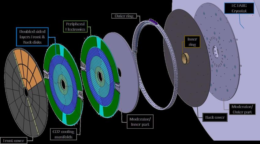
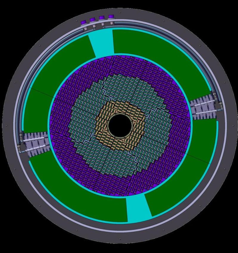
HGTD in a Nutshell Features and Motivations: • High Granularity Timing Detector (HGTD) new detector capability in the forward region (2.4 < < 4) • Mitigate pile-up with timing information: 30 ps to 50 ps resolution per track at the beginning and the end of life time • Track-to-vertex association is greatly improved enhance performance for jet and lepton reconstruction • Capability to provide bunch-by-bunch luminosity counts • Technology: Silicon based LGAD (Low Gain Avalanche Detector) TDR submission to LHCC in April
Layout and Overview 3 Rings: Inner, Middle & Outer ranging rom 12 – 64 cm radius Max radiation level specified: • NIEL: 2.5x10¹⁵ 1 MeV neq/cm2 (including SF 1.5) • TID: 2 MGy (including 2 x SF of 1.5 for low dose effect uncertainty) Replacement strategy after 1000 fb-1 for Inner Ring (LS4, LS5) and 2000 fb-1 for Middle Ring (LS5) Frontend readout features: - FE design in 130 nm CMOS (ALTIROC) - Hit data stream separated from Luminosity measurement stream - FE channel integrates amplification, discrimination, TDCs and digital FE blocks - Selectable data stream e-link bandwidth Block diagram of the transmission path - PEB lpGBT & VTRx+ for optical links ALTIROC : Atlas LgadTiming Integrated ReadOut Chip with backend systems PEB: Peripheral Electronic Board 26-28 May 2020
HGTD Modules
 Module consists of:
 • Sensor of 15x30 array of 1.3x1.3 mm2
 pad size
 • 2 ASICs of 15x15
 • Bump bond connection (SnAg)
 • Module flex with wire bond
 interconnects to the FE and
 connectors to the PEB
Cross section of a 2x2 LGAD array • HV bias supply up to 800V Magnification of a 15x15 arrary from HPK

 Timing resolution per hit < 65 ps at end of life time

R&D program so far confirms that the goal is achievable and the multiplication factor loss due to
 radiation effects is mitigated by pushing the HV up to ~700V
26-28 May 2020
Further details will be presented by:
A. Camplani
F. Le Goff

 26-28 May 2020
Trigger Scheme at HL-LHC
 Trigger designed to cope with the ultimate configuration: L = 7.5 1034 cm-2s-1 & µ of 200
Two possible schemes have been defined for the Phase-2 Upgrade:
1. A baseline architecture composed of a hardware-based Level-0 (L0) trigger running at 40 MHz
 input rate and a CPU farm-based Event Filter (EF) assisted by hardware-based track
 reconstruction and running at 1 MHz input rate.
2. An evolved version of the baseline architecture where an intermediate Level-1 (L1) trigger with up
 to 4 MHz input rate provides an additional filtering step between the Level-0 and Event Filter. In
 this scenario, the EF input rate is reduced to 800-600 kHz compared to the baseline scenario.
 Schematic of the baseline design Associative-memory-based tracking sequence
 performed by the Hardware Track Trigger (HTT)

26-28 May 2020
Trigger Possible Evolution Options considered for the EF at the TDR: a) a Hardware-based Tracking system for the Trigger (HTT) based on FPGAs and custom designed Associative Memory (AM) ASICs, b) Commodity CPU-based servers, c) Systems based on accelerators (general purpose GPUs), d) Future architectures based on devices integrating machine learning capabilities. Status quo and possible directions: Recent investigations demonstrated that software based tracking on standard CPU could fit up to PU 140 but would require early deployment of the complete CPU contingent foreseen for PU 200. ‐ It would be a fallback solution in case HTT would be late at the beginning of Run 4 ‐ However software tracking could never replace HTT at L1 due to latency constraints ‐ This promising result triggered the comparative study of cost and performance of an alternative architecture with commodity EF track also for PU of 200 “Evolved” trigger scenario for ITk Pixel may evolve to a Regional Readout new features into the FE chip: ‐ Less readout cables for Pixel Outer system ‐ Less back-end readout channels ‐ Question still open whether partially implementable for Run 4 and optimally where? ‐ Innermost layer replacement readout chip may evolve with RR feature implemented 26-28 May 2020
Further details will be presented by:
G. Auzinger

 26-28 May 2020
ATLAS L-Upgrade Target: precision of ~1% on integrated L Lessons learnt from Run-2 : sub-% uncertainty on each of: Redundancy across diverse luminometers • van der Meer calibration Aging effect mitigated with calibration/correction • calibration transfer from vdM to physics Afterglow minimized / corrected • Long-term stability/consistency BCM’ readout chain Diamond sensor pads L-Upgrade: BCM’ • Fast, bbb safety system for ITk (beam abort) • Background monitoring • Luminosity measurement Diamond sensor technology + fast analog readout (Calypso) + with picoTDC sampling Installed in the ITk Inner Pixel System (IS) at ~1.9 m from IP Options considered Si-BCM': adding silicon sensors to complement BCM’ (possible ATLAS- CMS collaboration); Pixel Lumi Ring (PLR) an additional Pixel ring in the IS devoted to Luminosity measurement L-Upgrade: LUCID-3 fiber detector (Based upon lessons from Lucid-2 at Run-2 and Run-3) • Both PMT and Fiber technology are under consideration for Run-4 • Two main factors to control for Lucid-3: hit saturation and gain-monitoring • Calibration of PMTs with Bi source has proven efficient in Run-2 Prototype fiber detector • Charge counting likely becomes more relevant than Hit counting algorithms with Bi calibration L-Upgrade: HGTD Using a Pixel Cluster Counting (PCC) method. 26-28 May 2020
Concluding Remarks • ATLAS Upgrade activities are dense in terms of development, construction, integration and installation – Only snapshots presented here. • Installation during LS3 (not reported here) will have to cope with many parallel activities in the experimental cavern. Some sub-systems are more demanding than others. • The progress so far is impressive in many areas. Not in R&D anymore (HGTD still to be approved) most are in prototype or in pre-production phase while few are starting the production. • Covid-19 pandemic is mostly affecting all the Upgrade activities Impact? Last remarks: • As usual devil is behind the details The earlier potential issues are caught the better ‐ Design and prototypes associated to qualification and QA is mandatory. ‐ Set of reviews with expert panels allows to progress steadily : SPR, PDR, FDR, PRR and PAR. ‐ Major decisions with crosslinked impact are addressed with task forces and endorsed at the management level. ‐ As for CMS yearly detailed reports are made to P2UG and tracked down (progress, issues, decision path and schedule). • Schedule is certainly the visible part of the “iceberg” and therefore tracking the milestones wrt the baseline is an essential tool for mapping the progress. 26-28 May 2020
ITk Pixel Local Support and Mechanics
 Work progress from local support towards loading and integration with services

 Handling frame of OE Half ring with embedded cooling pipe
 an IS ring L0/L1

OB inclined ring OB flat section longeron
integration procedure supporting 36 Quad
Inside a half shell modules
 Cooling interface

 26-28 May 2020
ITk Pixel – Data Transmission While looking forward the transmission chain with GBCR2,ITkPixV1,and lpGBT tests Results are very encouraging as of now: o Tests with a long chain such as RD53a + Rd53b_cdr + Flex + 6m Twinax + DAQ o Simulations with GBCR2 + 6mTwinax + 1m Flex Uplink tests @ 1.28 Gbps w/o GBCR2 Data when Cmd pre-emph=0 Data when Cmd pre-emph=3 @ 160 Mbps @ 1.28 Gbps Jitter = 156 ps Simulations Jitter = 60 ps w/ GBCR2 26-28 May 2020
ITk Strip – Modules
ITk Strip – Module Testing
ITk Strip – Power Board

 • Development of power board mass tester for QC and reception testing at module
 sites is progressing well
 • Upcoming batch of 250 barrel power boards will be used to finalize and stress test
 the system
 Charge pump HV filter
 circuit
DCDC circuit covered LinPOL12V
 by Shield box

 HVMux
 AMACv2a
 Module noise peak associated to the
 Hybrid connections power board now fixed with new layout
Trigger and Physics Goals
 Potential to be fully exploited for the main physics drivers (as in the TDR)

26-28 May 2020
Trigger and Physics Goals
 Flow of the Physics Goals to the Hardware

26-28 May 2020
You can also read