5G planar branch line coupler design based on the analysis of dielectric constant, loss tangent and quality factor at high frequency - Nature
←
→
Page content transcription
If your browser does not render page correctly, please read the page content below
www.nature.com/scientificreports
OPEN 5G planar branch line coupler
design based on the analysis
of dielectric constant, loss tangent
and quality factor at high frequency
Nor Azimah Mohd Shukor & Norhudah Seman*
This study focuses on the effect of different dielectric properties in the design of 3-dB planar branch
line coupler (BLC) using RT5880, RO4350, TMM4 and RT6010, particularly at high frequency of
26 GHz, the fifth generation (5G) operating frequency. The analysis conducted in this study is based
on the dielectric constant, loss tangent and quality factor (Q-factor) associated with the dielectric
properties of the substrate materials. Accordingly, the substrate that displayed the best performance
for high frequency application had the lowest dielectric constant, lowest loss tangent and highest
Q-factor (i.e., RT5880), and it was chosen to enhance our proposed 3-dB BLC. This enhanced 3-dB
BLC was designed with the inclusion of microstrip-slot stub impedance at each port for bandwidth
enhancement, and the proposed prototype had dimensions of 29.9 mm × 19.9 mm. The design and
analysis of the proposed 3-dB BLC were accomplished by employing CST Microwave Studio. The
performance of scattering parameters and the phase difference of the proposed BLC were then
assessed and verified through laboratory measurement.
Due to the rapid advancements in wireless communications, a sophisticated communication system that includes
high-performance devices necessary to deploy next (i.e., fifth) generation (5G) technologies. This system requires
devices that further perfect wireless communication between anything, anywhere and at any t ime1. The 5G were
deployed in several countries including South Korea, the United Kingdom, Germany and the United States and
many more countries are expected to deploy 5G soon and the high demand for 5G technology, which require
24/7 ubiquitously high-speed connectivity become a significant challenge for researchers and engineers involved
in the development of radio frequency (RF) and microwave components, antenna design, and network planning.
Butler matrix design is particularly high-demand in 5G application because the Butler matrix can be employed
to support the control capability of beam-forming and electric scanning a ntennas2.
The Butler matrix was first introduced by Jesse Butler and Ralph Lowe3 and the beam-forming network creates
multiple fixed overlapping beams to cover the designated angular a rea4. Since it is an N × N passive reciprocal
network, it can be used to transmit and receive signals5,6. There are several properties associated with the Butler
matrix, including inputs that are isolated from each other, phases of N outputs that are linear with respect to
position and a phase increment between the outputs that depends on the selection of i nput4. The Butler matrix
is also capable of beam-steering with uniform amplitude and adequate phase difference between consecutive
output ports5. The power at the input port of the Butler matrix is equally distributed to the output p orts4 and
the configuration of the Butler matrix essentially consists of passive components such as a branch line coupler
(BLC), a phase shifter and c rossover7,8. A non-conventional configuration BM has been proposed by Babale
et al.9, where the BM was constructed without using crossover and phase shifter, however it was not practical
for cascaded BM due to the position of input and output ports, which may lead to the connection issues. As the
most critical component in the Butler matrix configuration, the BLC designed during the first stage must dis-
play good performance. Since a BLC is only capable offering narrowband performance, many studies related to
bandwidth improvement have been performed. The defect ground structure (DGS) technique can be employed
under the branch arm of the BLC for to improve bandwidth10. Employing the DGS technique able to enhance
the bandwidth of the BLC design10 by 8.2% compared to conventional BLCs.
Wireless Communication Centre (WCC), School of Electrical Engineering, Universiti Teknologi Malaysia (UTM),
81310 UTM Johor Bahru, Johor, Malaysia. *email: huda@fke.utm.my
Scientific Reports | (2020) 10:16115 | https://doi.org/10.1038/s41598-020-72444-2 1
Vol.:(0123456789)
www.nature.com/scientificreports/
Then, a dumbbell-shaped DGS was etched on the ground plane of another B LC11 design. In the design, a
120Ω transmission line was used to replace the quarter-wavelength 150Ω transmission line. The performance
of this design indicated that the good results could be achieved within a frequency range of 1.85–3.35 GHz
with a bandwidth enhancement of approximately 20%. However, the disadvantage of using a DGS is that it
is only suitable to be implemented with the high line impedance. Another technique that use a slotted line
on a BLC was introduced to further improved bandwidth12. The slotted line was placed at the ground plane
and positioned beneath the vertical branches of the BLC design. It was concluded that slot dimensions (i.e.,
W × L) of 0.7 mm × 11.5 mm resulted in the best BLC performance within a frequency range of 3.5–4.7 GHz12.
This BLC design12 has improved bandwidth by 80% compared to conventional BLCs. Another 3-dB BLC with
improved bandwidth proposed by Jin and X u13 by introducing the artificial magnetic conductor (AMC). The
design comprised of a spacer with hollow interspace in the middle layer that sandwiched by AMC patches at
the upper layer and microstrip coupler which printed on the upper surface of the bottom substrate layer. This
multilayered coupler structure faced misalignment between each layer and air gap in the fabrication stage that
led to a significant impact on the performance for high frequency applications. Thus, the implementation of a
single substrate in the coupler design at high frequency is preferable.
Another crucial aspect in designing the coupler is the planar dielectric material, which is also known as the
substrate. The parameters of the substrate are not only focused on the degree of design miniaturization but also
influences the quality factor (Q-factor) of the components. The effect of different dielectric constants, ɛr towards
coupler size has been presented by Letavin Denis et al.14 concerning Rogers RT (ɛr = 3) and FR-4 (ɛr = 4.4), and
design frequency of 2 GHz. The authors stated that FR-4 substrate has a better effect on the miniaturization of
coupler compared to Roger RT due to its higher dielectric constant. However, miniaturization is not a concern
in the design at high frequency. The c omponents7,14,15 designed on FR-4 substrate due to its low cost, with FR-4
having a high loss tangent. Since FR-4 displays a high loss tangent, it may degrade the Q-factor of the design,
which leads to the degradation of performance compared to the performance of the designs with RO4003C6
and RT587016. Authors have added that the measured performance is also degraded due to several other factors,
such as conduction losses and dielectric l osses7, 17. Hence, FR-4 is not suitable for high-frequency design due to
its high dissipation factor, which results in higher losses as the frequency increases18. Therefore, the FR-4 sub-
strate is not considered suitable for high operating frequency design. Thus, most of the researchers are having a
tendency to select the high-performance substrate material over FR-4 substrate for high frequency design due
to this impact of high loss tangent, which will significantly affect the performance of the circuit. The dielectric
losses of the substrates are closely related to the dissipation factor and the loss tangent, which are proportional
to the frequency17. Despite, loss tangent seems to be a clear factor in the substrate selection, other dielectric
properties’ effects toward the design such as dielectric constant and Q-factor are required to be carefully studied
at high frequency together with loss tangent to ensure a good performance can be accomplished particularly
for microstrip implementation. The effects due to dielectric constant and Q-factor cannot be known from the
manufacturer datasheet without systematic study and analysis.
The remainder of this paper is organized in the following manner. Next section introduces the analysis of
different substrates having different properties with respect to the dielectric constant, loss tangent, and Q-factor
associated with dielectric properties and their relationship to BLC performance was observed. The enhanced BLC
design was then proposed with the implementation of microstrip-slot stub impedance at each port’s transmission
line. The performance was simulated and measured. It was then compared to the conventional design and other
designs using different techniques, and discussed thoroughly.
Methods
Selecting the best substrate to be incorporated into the design is crucial, especially at higher operating frequencies
used in 5G wireless communication applications. Therefore, in this study, the analysis of a single-section planar
BLC with different substrates was conducted. Questions arise regarding which substrate among the available
high-performance substrates offers the best performance for the 3-dB BLC design at the designated frequency.
The analysis in this study is based on the dielectric constant, loss tangent, Q-factor and their relationship to
BLC performance.
Analysis of different substrates. The characteristics of different substrates can affect the overall perfor-
mance of the design. Four different substrates were selected for analysis, including RT5800, RO4350, TMM4 and
RT6010, which were chosen due to their excellent performance at higher frequencies. Each of the four substrates
has a different dielectric constant and loss tangent, while the thickness of the substrate was fixed at 0.254 mm.
The properties of each substrate are summarized in Table 1.
RT5880, which is made of glass microfiber reinforced polytetrafluoroethylene (PTFE) composite, displayed
the lowest dielectric constant (2.2) among all the chosen high laminating frequency substrates, the lowest loss
tangent (0.0009), and a negative thermal coefficient of − 125 ppm/°C19. Since RT5880 has a low dielectric con-
stant, it is suitable for high frequency applications because the electrical losses and dispersion is considered to be
minimal19. Meanwhile, the RO4350 substrate, which is a woven glass reinforced hydrocarbon ceramic laminate
displayed second-lowest dielectric constant (3.66), the highest loss tangent (0.0037), and the highest positive
thermal coefficient of + 50 ppm/°C20. This substrate provided tight control of the dielectric constant and displayed
low loss19. The third substrate was TMM4, which is composed of a ceramic thermoset polymer composite with a
dielectric constant (4.7), the second-lowest loss tangent (0.0020), and a low thermal coefficient of + 15 ppm/°C21.
The electrical and mechanical properties of TMM4 laminates combine many of the benefits of both ceramic
and traditional (PTFE) microwave circuit laminates21. Finally, the RT6010 substrate had the highest dielectric
Scientific Reports | (2020) 10:16115 | https://doi.org/10.1038/s41598-020-72444-2 2
Vol:.(1234567890)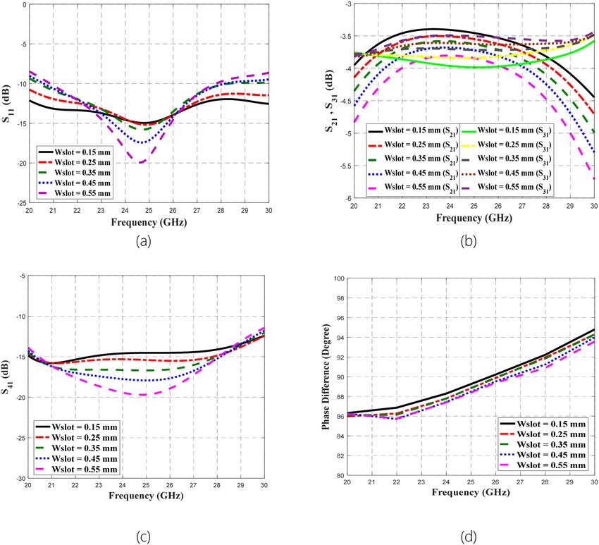
www.nature.com/scientificreports/
Substrate Material Dielectric Constant, ɛr Loss Tangent, tan δ Thickness h (mm) Thermal Coefficient (ppm/°C) Condition (GHz)
Glass microfiber reinforced PTFE
RT5880 2.2 0.0009 0.254 − 125 8–40
composite
Woven glass reinforced hydrocarbon
R04350 3.66 0.0037 0.254 + 50 8–40
ceramic
Ceramic thermoset polymer com-
TMM4 4.7 0.0020 0.254 + 15 8–40
posite
RT6010 Ceramic PTFE composite 10.7 0.0023 0.254 − 425 8–40
Table 1. The substrates with the different materials and dielectric properties.
constant (10.7) with negative thermal coefficient of − 425 ppm/°C18. Furthermore, this substrate also displayed
low loss with loss tangent of 0.002322.
Generally, when selecting a dielectric material during the design process, two parameters are considered,
including the dielectric constant and loss tangent. The loss tangent, tan δ defines the measure of signal loss as
the signal propagates through the transmission line, and can be expressed as (1)23,24:
ωεr′′ + σ
tan δ = (1)
ωεr′
where εr′ and εr′′ are the real and imaginary part of the complex relative permittivity, εr∗, respectively. Meanwhile,
ω and σ are angular frequency and conductivity, respectively with conditions of εr′′ ≥ 0 and εr′ ≫ εr′′ . The real
part of εr∗, which is εr′ associated to the ability of a material to store the incident electromagnetic (EM) energy
through wave propagation, while, the imaginary part of εr∗ is denoted by εr′′ related to the degree of EM energy
losses in the material. Thus, εr′ and εr′′ are also known as the dielectric constant, ɛr and the loss factor, respectively.
At high frequencies that were considered in this proposed work, the substrate’s loss tangent, tan δ can be simpli-
fied to εr′′ /εr′ . It is also known as the dissipation factor that describes the angle difference between capacitance
current and voltage. Hence, a lower loss tangent is required in the substrate to ensure low dielectric loss and
low dielectric absorption25. These two parameters, ɛr and tan δ are directly related to the Q-factor due to the
dielectric, Qd that can be expressed as (2)26:
√
εeff
Qd = 27.3 (2)
αd 0
where the εeff , λ0 and αd are the effective dielectric constant, the wavelength in the air and dielectric loss, respec-
tively. The εeff can be defined by (3)23:
εr + 1 εr − 2 1
εeff = + √ (3)
2 2 1 + 12h/Wm
where h and Wm are the thickness of the substrate and the width of the microstrip transmission line, respectively,
while, the dielectric loss, αd can be expressed as (4)26:
εr εeff − 1 tan δ
αd = 27.3
(4)
εeff (εr − 1) o
Thereafter, an analysis of the Q-factor associated with the material’s dielectric properties, Qd was performed
through calculation implementing (2)–(4) to observe the effect of different substrates, including RT5880,
RO4350, TMM4 and RT6010, which have a different dielectric constant, ɛr and loss tangent, tan δ. The width of
the microstrip transmission line, Wm that correspond to 50Ω was used in this analysis. The relationship between
Qd and the different ɛr of RT5880, RO4350, TMM4 and RT6010 substrates, and the relationship between Qd and
tan δ are depicted in Figs. 1 and 2.
As presented in Fig. 1, RT5880, RO4350, TMM4 and RT6010 substrates have Qd values of 1302.79, 302.56,
549.70 and 458.69, respectively. It is important to note that Qd generally decreases as the value of εr increases as
depicted by the proportional correlation between Qd and εeff , which is calculated using Eq. (2), where RT5880
has the highest Qd and the lowest εr . However, this trend does not apply to RO4350 that had the second-lowest
εr and the lowest performance of Qd. Hence, by referring back to Eqs. (2) and (4), setting aside the dielectric
constant, εr , Qd is inversely proportional to dielectric loss, αd. Consequently, this αd is determined by εr and
tan δ as expressed in Eq. (4). Since αd is proportional to tan δ, and Qd is inversely proportional to αd, thus Qd is
inversely proportional to tan δ. Meanwhile since αd is a function of εr , the influence of tan δ towards Qd is greater
compared to εr , which can be observed from the plot in Fig. 2. Referring to Fig. 2, the value of Qd decreases as
the value of tan δ increases. Therefore, even though RO4350 has the second-lowest εr , it has the highest tan δ
among the substrates, which led to the lowest Qd performance.
Generally, this behavior can be explained by the characteristics of the εr that is influenced by ionic or elec-
tronic polarization, which generates αd in the presence of electromagnetic w ave27. The increasing value of
εr provides a higher αd value as the electric field intensity inside the dielectric layer increases23. RT5880 and
RT6010 have polytetrafluoroethylene (PTFE) in their composition, while TMM4 has a polymer with low thermal
Scientific Reports | (2020) 10:16115 | https://doi.org/10.1038/s41598-020-72444-2 3
Vol.:(0123456789)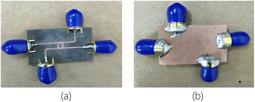
www.nature.com/scientificreports/
Figure 1. The relation between the Q-factor associated with the dielectric properties, Qd and dielectric constant
of the different substrates.
Figure 2. The relation between the Q-factor associated with the dielectric properties, Qd and loss tangent, tan δ.
Figure 3. The design of the single-section 3-dB branch line coupler.
conductivity, an excellent coefficient of thermal expansion (CTE), and low processing temperature, which results
in low αd 28 as presented in Table 1. While, glass is a good thermal and homogeneity insulator, it also displays a
high dielectric loss28. To obtain a lower αd value and maintain the advantages of glass, glass-reinforced ceramics
can be used as displayed by R0435028. In any event, the dielectric loss of R04350 is still higher than RT5880,
TMM4 and RT6010. Following this analysis of the four substrates, further analysis was performed by employing
a single-section planar 3-dB BLC design.
Analysis of BLC using different substrates. Figure 3 presents the design of the single-section 3-dB
BLC. The common microstrip equation is denoted as (5), which was used to compute Wo, Wm1 and Wm2, where
Wo and Wm2 refer to the characteristics of 50Ω, while Wm1 refer to those of 35Ω23:
Scientific Reports | (2020) 10:16115 | https://doi.org/10.1038/s41598-020-72444-2 4
Vol:.(1234567890)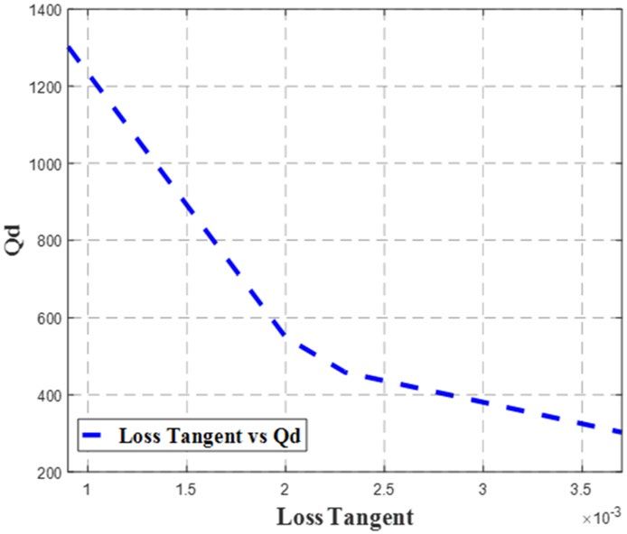
www.nature.com/scientificreports/
Substrates/dimensions (mm)
Parameters RT5880 RO4350 TMM4 RT6010
Wm1 0.8 0.65 0.5 0.25
Wm2 1.1 0.9 0.6 0.5
Wo 0.8 0.65 0.5 0.25
λg/4 2.12 1.71 1.54 1.08
Table 2. Dimensions of single-section 3-dB BLCs using different substrates.
Figure 4. The reflection coefficients, S11 of the 3-dB BLC with different substrates.
Wm 2 εr 0.61
= B − 1 − ln (2B − 1) + ln (B − 1) + 0.39 − (5)
h π 2εr εr
where constant B can be expressed as (6)23:
377π
B= √ (6)
2Z0 εr
where Z0 is the characteristic impedance.
The guide wavelength, λg was then determined by (7)29:
c
g = √ (7)
f εeff
where c and f are the speed of light and design frequency, respectively. The properties for each substrate were
used to design the 3-dB BLC, and the dimensions of the designed couplers were computed and optimized, which
are summarized in Table 2. The performance of each BLC was then assessed based on S-parameters, phase dif-
ference and bandwidth.
The performance of each BLC was then assessed based on S-parameters, phase difference and bandwidth via
simulation through the use of Computer Simulation Technology (CST) Microwave Studio software. Transient
Solver tool was utilized with frequency range setting between 20 to 30 GHz and open boundary condition to
calculate the energy transmission between various ports of the design structure. Figure 4 illustrates the reflection
coefficient performance, S11 of the designed BLC with different substrates, which revealed that the S11 of the BLC
designed with the RT5880 substrate was less than − 10 dB within a frequency range of 20.54–30 GHz. Meanwhile,
the BLC design that employed the RO4350 substrate showed the performance of S11 was below − 10 dB across
21–30 GHz. In addition, the use of TMM4 and RT6010 offered S 11 values that were less than − 10 dB in the ranges
of 21.1–30 GHz and 22.55–30 GHz, respectively. Hence, the best S 11 performance with the relatively broadest
bandwidth and lowest S11 at 26 GHz, which is shown by the design that employed RT5880, which has the lowest
εr and lowest tan δ among all four substrates was expected to have the lowest loss.
Figure 5 shows the transmission coefficient of S21 when different substrates were used in the design of the
BLC. Similar S21 performance of − 3 dB with ± 1 dB deviation were obtained for RT5880, RO4350, TMM4, and
RT6010 for slightly different frequency ranges of 21.14–30 GHz, 21.9–30 GHz, 23.18–30 GHz and 24.28–30 GHz,
respectively. Compared to S 11 performance, BLC design with RT5880 displayed the widest frequency range of
8.86 GHz with S 21 performance of − 3 dB ± 1 dB. Meanwhile Fig. 6 depicts the coupling output, S 31 that speci-
fies the ratio of input power, P 1 to the coupled power, P
3 for BLC design that utilized different substrates. The
Scientific Reports | (2020) 10:16115 | https://doi.org/10.1038/s41598-020-72444-2 5
Vol.:(0123456789)
www.nature.com/scientificreports/
Figure 5. The transmission coefficients, S21 of the 3-dB BLC design using different substrates.
Figure 6. The coupling performance, S31 of the BLC design by using different substrates.
results of our analysis indicated that the performance of S 31 was –3 dB ± 0.9 dB within a frequency range of
20–30 GHz when RT5880 substrate was used in the design, while, the coupling performance was –3 dB ± 1 dB
when the RO4350 substrate was used in a range of 20–28.74 GHz. Furthermore, similar performances of S 31 were
achieved when the design utilized TMM4 and RT6010 substrates, which were − 3 dB ± 1 dB in a frequency range
of 20.34–28.62 GHz and 21.28–27.07 GHz, respectively. Hence, a coupling coefficient of 3-dB with the lowest
deviation across the widest frequency range was achieved by the BLC design utilized onto RT5880 substrate.
The next important analysis is associated with S41 performance, which involves the responses obtained from the
BLC design with different substrates as depicted in Fig. 7. In this design, the lowest isolation performance was
set to be 10 dB. As shown in Fig. 7, the performance of S 41 was less than − 10 dB within a frequency range of
20–30 GHz for the design that employed all substrates. In this analysis, the lowest S41 performance at 26 GHz
shown by the design that employed RT5880.
Therefore, the analysis proceeded to consider the phase difference between output ports. In this design,
the deviation of the phase difference between the output ports was set to ± 2° from the ideal of 90°. Based on
the phase difference analysis shown in Fig. 8, a BLC phase difference of 90° ± 2° are demonstrated by designs
that employed RT5880, RO4350, TMM4 and RT6010 substrates across slightly different frequency ranges of
24.52–30 GHz, 25.52–29.17 GHz, 25.5–28 GHz and 24.81–27.73 GHz, accordingly. Similarly, as in the analysis
of S11, S21, S31 and S41, the design with RT5880 displayed the best phase performance across the widest frequency
range, which is likely because it has the lowest εr and lowest tan δ. The performances of S11, S21, S31, S41 and the
phase difference between output ports are summarized in Table 3. The Q-factor associated with the material’s
dielectric properties, Qd that was obtained through the analysis of those dielectric properties is presented in
Table 3 for further comparison and analysis.
Table 3 shows that the widest bandwidth performance of 5.48 GHz (21.1%) was achieved when the RT5880
substrate was used in the BLC design. Referring to Table I, RT5880 has the lowest εr of 2.2 and lowest tan δ of
0.0009 which resulted in the highest Qd of 1302.79. Meanwhile, RT6010 displayed the narrowest bandwidth
performance of 2.26 GHz (8.7%) and it has the highest εr of 10.7 and second-highest tan δ of 0.0023, which lead
to a lower Qd of 458.69. The RO4350 substrate with the highest tan δ of 0.0037 and the second-lowest εr of 3.6
and displayed the lowest Qd of 302.56, though it also had the second-widest bandwidth performance of 3.22 GHz
Scientific Reports | (2020) 10:16115 | https://doi.org/10.1038/s41598-020-72444-2 6
Vol:.(1234567890)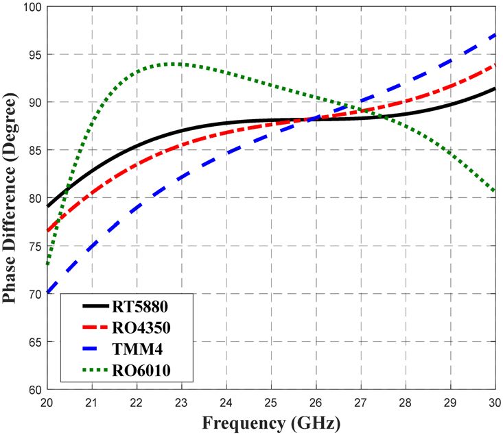
www.nature.com/scientificreports/
Figure 7. The S41 performance of the 3-dB BLC design with different substrates.
Figure 8. The phase difference performance of the 3-dB BLC design with the use of different substrates.
Substrates/dimensions (mm)
Parameters RT5880 RO4350 TMM4 RT6010
S11 (dB) < − 10 < − 10 < − 10 < − 10
S21 (dB) −3±1 −3±1 −3±1 −3±1
S31 (dB) − 3 ± 0.9 −3±1 −3±1 −3±1
S41 (dB) < − 10 < − 10 < − 10 < − 10
Phase Difference (Degree) 90 ± 2 90 ± 2 90 ± 2 90 ± 2
Operating Frequency (GHz) 24.52–30 25.52–28.74 25.5–28 24.81–27.07
5.48 3.22 2.5 2.26
Bandwidth, GHz (%)
(21.1) (12.4) (9.6) (8.7)
Qd 1302.79 302.56 549.70 458.69
Table 3. The performance of 3-dB BLC design with different substrates and the respective Qd.
(12.4%). Even though a lower tan δ significantly contributes to a higher Qd compared to εr , results indicated that
the εr is a primary factor in the determination of optimal bandwidth performance with an inversely proportional
relationship. The εr of a material represents the ability of that material to store electrical energy in the presence of
an electrical field, whereas, when the frequency increases, the losses in the substrate begins to reduce the ability of
the dielectric material to store energy. Therefore, it can be concluded that the bandwidth performance increases
as the dielectric constant decreases, while the high dielectric constant substrate may lose its ability of storing
energy. Thus, based on the results of our analysis, the substrate with a low dielectric constant and a low tan δ,
which contribute to the respective high bandwidth and high Q-factor is the most suitable for 5G applications
at high frequencies, and in this case, a design frequency of 26 GHz that uses the RT5880 substrate was selected.
Scientific Reports | (2020) 10:16115 | https://doi.org/10.1038/s41598-020-72444-2 7
Vol.:(0123456789)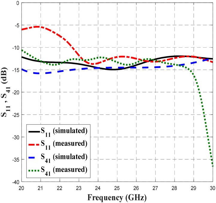
www.nature.com/scientificreports/
Figure 9. The proposed 3-dB BLC with the implementation of microstrip-slot stub at each port; (a) top view
and (b) bottom view.
Design of 3‑dB BLC with microstrip‑slot stub. This section discusses the proposed wideband 3-dB
BLC design, as depicted in Fig. 9, with the implementation of a microstrip-slot stub for bandwidth improvement
over that of conventional BLC designs, as shown in Fig. 3 by using CST Microwave Studio with the utilization
of Transient Solver tool, frequency range setting between 20 to 30 GHz and open boundary condition. The best
substrate was RT5880 based on the analysis of its dielectric properties, and was thus chosen for the design. The
proposed microstrip-slot stub impedance was placed at each port at a distance, L1 from the BLC. By tuning these
microstrip-slot stub impedances, better matching can be achieved to ensure maximum power is transferred from
the source, and a minimum signal is reflected from the load, which consequently enhances the b andwidth30,34.
Generally, the input impedance of the stub, Yin can be written as (8)31:
Yin = jY0 tan θstub (8)
where Y0 and θstub are the stub admittance and the electrical length of the stub, respectively, and the θstub can be
expressed as (9)31:
ω0
θstub = βLs = Ls (9)
Vpstub
where ω0, Ls and Vpstub are the angular frequency, the length of stub and the phase velocity of the stub, respectively.
By comparing Y = ωC to Eq. (8), the length of the stub, Ls can be obtained in (10)31:
1 ω0
ω0 C = tan Ls (10)
Zstub Vpstub
where Zstub is the characteristic impedance of the stub. It was stated that junction discontinuities can be avoided
when the length of stub impedance is half the wavelength28. However, the parameters still need to be optimized
to achieve optimal performance. To achieve optimal performance, a stub with a higher impedance is required32.
Furthermore, stub impedance can form reflection zeroes at equal distances on both sides of the ports30. The
distance of the stub impedance of the proposed BLC design is defined as L1. Referring back to the common match-
ing technique that employs the s tub23, the load impedance, ZL representing the BLC can be expressed as (11):
1
ZL = = RL + jXL (11)
YL
where YL, RL and XL are the load admittance, the real part of load impedance and the imaginary part of load
impedance, respectively. Therefore, the impedance at a distance, L1 from the load (BLC) is given in the (12) and
(13):
RL + jXL + jZ0 t
ZL1 = Z0
(12)
Z0 + j RL + jXL t
and
t = tan βL1 (13)
Let the admittance of stub impedance at a distance, L1 be expressed as (14):
1
YL1 = G + jB = (14)
ZL1
where parameters G and B can be defined by (15) and (16), respectively, by using (13) and (14):
Scientific Reports | (2020) 10:16115 | https://doi.org/10.1038/s41598-020-72444-2 8
Vol:.(1234567890)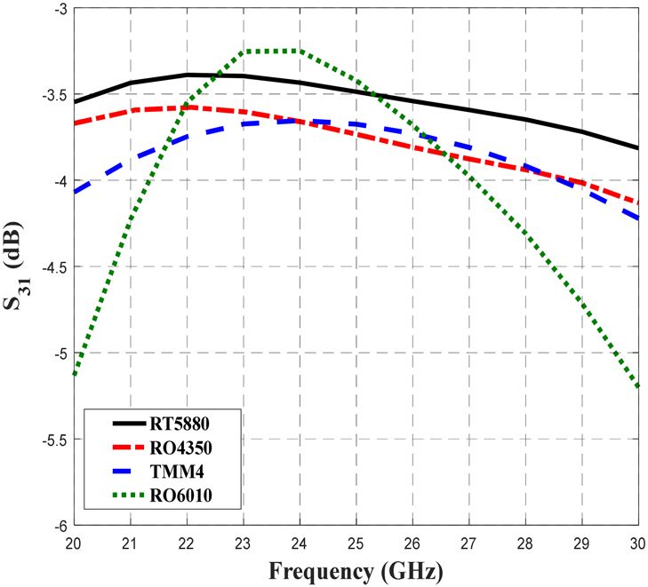
www.nature.com/scientificreports/
Parameters Dimension (mm)
Wm1 1.09
Wm2 0.8
Wm3 0.7
Wslot 0.15
L1 0.65
Ls 0.85
Wo 0.8
λg/4 2.12
Table 4. Dimensions of proposed 3-dB Branch Line Coupler.
RL 1 + tan2 βL1
G= (15)
RL2 (XL + Z0 tan βL1 )2
and
RL2 tan βL1 − (Z0 − XL tan βL1 )(XL + Z0 tan βL1 )
B= (16)
Z0 RL2 (XL + Z0 tan βd)2
Then, by equating G = Y0 = 1/Z0 and from (13)23,
RL 1 + t 2
1
= 2 (17)
Z0 RL + (XL +)
Therefore, the value of t can be expressed as (18):
�
2 2
XL ± RL [(Z0 −RZ L ) +XL ]
0
t= RL −Z0 , for RL �= Z0 (18)
−XL ,
for RL = Z0
2Z0
Thereafter, by assuming RL = Z0 and by using t = tan βL1 = tan 2π
L1, the distance of stub impedance from
BLC, L1 can be determined using (19):
1 −1
L1
= 2π 1
tan t, −1
for t ≥ 0 (19)
2π π + tan t , for t > 0
A narrow slot line is then employed at the ground plane underneath the microstrip stub to form microstrip-
slot stub impedance because the use of the slot line can improve the bandwidth performance due to its slow-
wave characteristic. The implementation of slot-line on the ground plane disturbs current distribution and this
disturbance changes the characteristics of the transmission line, such as capacitance and inductance, to produce
the slow-wave characteristics, which can increase the phase velocity delay. The characteristic impedance of the
microstrip-slot stub can be determined through the use of the microstrip-slot line impedance, Zm−s equation
as expressed in (20)33:
Zm−s = 18.22(Wslot )2 + Zm (20)
Obtaining the initial dimensions through calculation, this proposed BLC was simulated and optimized
accordingly. The optimized dimensions of the coupler, as depicted in Fig. 9 were Wo = 0.8 mm, Wm1 = 1.09 mm,
Wm2 = 0.8 mm, Wm3 = 0.7 mm, Wstub = 0.18 mm, Wslot = 0.15 mm, L1 = 0.65 mm, Ls = 0.85 mm and length of each
branch, λ/4 = 2.12 mm. The dimensions of the proposed BLC are summarized in Table 4. The next objective is
to verify the performance of the proposed BLC. Then, the proposed design was realized by employing the Roger
RO5880 substrate with dielectric constant, ɛr of 2.2, a substrate thickness, h of 0.254 mm, and an overall size of
29.9 mm × 19.9 mm. Figure 10 shows the fabricated prototype of the proposed BLC with slotted-stub impedance.
Measurement of 3‑dB BLC with microstrip‑slot stub. The measurement of the proposed 3-dB BLC
with microstrip-slot stub fabricated prototype was conducted using a vector network analyzer (VNA) to verify
its performance. Prior to the measurement, the two-port network calibration procedure of VNA is necessary
to remove its errors. The calibration was performed using the calibration standards involving the open, short,
match, and through35. Following the completed calibration procedure, the measurement of the proposed BLC
prototype was carried out with the setup as depicted in Fig. 11. Referring to the measurement setup, the selected
ports were connected directly to the VNA, while the unused ports were terminated with 50 Ω SMA termination.
Thereafter, a comparison was made in terms of the simulated and measured S-parameters and phase character-
istics.
Scientific Reports | (2020) 10:16115 | https://doi.org/10.1038/s41598-020-72444-2 9
Vol.:(0123456789)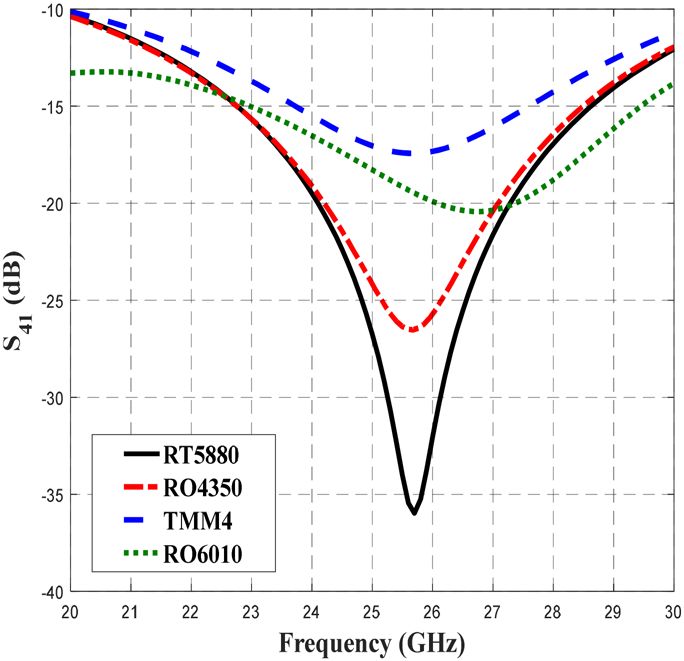
www.nature.com/scientificreports/
Figure 10. The photography of the proposed 3-dB BLC prototype with the implementation of microstrip-slot
stub impedance; (a) front view and (b) back view.
Figure 11. (a) Calibration standards36, and (b) the measurement setup of the proposed BLC using a vector
network analyzer (VNA).
Figure 12. The simulated and measured S11 and S41 of the proposed BLC.
Scientific Reports | (2020) 10:16115 | https://doi.org/10.1038/s41598-020-72444-2 10
Vol:.(1234567890)www.nature.com/scientificreports/
Figure 13. The simulated and measured S21 and S31 of the proposed BLC.
Figure 14. The simulated and measured phase difference of the proposed BLC.
Proposed BLC
Parameters Initial BLC (RT5880) Simulated Measured
S11 (dB) < − 10 < − 12 < − 11
S21 (dB) −3±1 −3±1 −3±1
S31 (dB) − 3 ± 0.9 − 3 ± 0.8 − 3 ± 0.9
S41 (dB) < − 10 < − 12 < − 11
Phase Difference 90° ± 2° 90° ± 3° 90° ± 4°
Operating Frequency (GHz) 24.52–30 20–28.7 22–30
Bandwidth (GHz) 5.48 (21.1%) 8.7 (34.8%) 8 (32%)
Table 5. The simulated and measured performance of the proposed 3-dB BLC design.
Results and discussion
Figures 12,13 and 14 depict the simulated and measured performance of the proposed BLC, which operated well
from 20 to 28.7 GHz and 22 to 30 GHz, respectively. As shown in Fig. 12, the simulated and measured S 11 and
S41 values were less than − 12 dB and − 11 dB, respectively. The value of − 10 dB and below used as the specifi-
cation to indicate a good transmission signal from the input port to the output port, where almost 90% of the
signal is being t ransmitted. Meanwhile based on the results presented in Fig. 13, the simulated and measured
transmission coefficients at the coupling port (S31) displayed a ± 1 dB deviation from the ideal value of 3 dB,
while, the simulated and measured transmission coefficients of S 21 depict the performance of − 3 dB ± 0.8 dB
and − 3 dB ± 0.9 dB, respectively. Meanwhile, the plotted responses in Fig. 14 indicate that the simulated and
measured phase differences between output ports were 90° ± 3° and 90° ± 4°, respectively. These S-parameters
and phase difference performance are summarized in Table 5 to provide a clear comparison.
Scientific Reports | (2020) 10:16115 | https://doi.org/10.1038/s41598-020-72444-2 11
Vol.:(0123456789)www.nature.com/scientificreports/
Figure 15. Parametric analysis on varied Wslot concerning (a) S11, (b) S21 and S31, (c) S41, and (d) phase
difference between output ports.
Based on the data in Table 5, the proposed BLC with microstrip-slot stub impedance at the ports’ transmis-
sion line appeared to result in better performance of S11, and S41 at a bandwidth was improved by approximately
2.52 GHz compared to initial single-section BLC design. Comparable transmission coefficients of S21 and S31
were observed between the proposed BLC and initial BLC designs. However, the phase difference between the
output ports of the proposed BLC has deviated slightly more (± 1°) than initial BLC designs, but it was still within
a reasonable performance range with respect to phase difference. Furthermore, performance of the simulated and
measured BLC with microstrip-slot stub impedance were consistent with one another, along with an operating
frequency that was slightly shifted. One of the main reasons that have been found affecting the measurement
results was a small discrepancy in the width of the microstrip-slot stub impedance. To prove this, simulation
on different widths of the microstrip-slot stub impedance was performed, analyzed, and discussed in the next
sub-section.
Parametric analysis on different widths of the microstrip‑slot stub impedance. Parametric
analysis on different widths of the microstrip-slot stub impedance concerning its microstrip stub width, Wstub
and slot line width, Wslot was performed via the use of CST Microwave Studio with a similar setting as in analysis
and design in the section of Methods. Initially, the parametric analysis was started by fixing Wstub to its optimal
dimension of 0.18 mm and varying Wslot between 0.15 mm and 0.55 mm. The effect of this varied Wslot was
observed through S-parameters and phase difference as depicted in the following Fig. 15.
The function of slot implementation is to broaden the bandwidth due to its slow-wave characteristics. Con-
cerning the bandwidth performance, it shows that from the plotted graphs in Fig. 15, the broadest bandwidth
was provided by the smallest value of Wslot (0.15 mm) compared to the largest value of Wslot (0.55 mm). Besides,
the smallest amplitude imbalance and phase imbalance were offered by 0.15 mm Wslot. Thus, the optimal Wslot
dimension is 0.15 mm for this proposed coupler design. Any discrepancy from this optimal width will lead to
deviation in the results of S-parameters and phase difference, in which the deviation trends can be observed
through the plotted graphs. By comparing the plotted varied Wslot graphs to the summarized measured results
in Table 5 and the assumption of fixed Wstub at 0.18 mm, it can be estimated that the fabricated coupler could
have 0.35 mm Wslot instead of 0.15 mm. Afterward, the next concern is the effect of the varied Wstub towards the
Scientific Reports | (2020) 10:16115 | https://doi.org/10.1038/s41598-020-72444-2 12
Vol:.(1234567890)www.nature.com/scientificreports/
Figure 16. The parametric analysis on varied Wstub concerning (a) S11, (b) S21 and S31, (c) S41, and (d) phase
difference between output ports.
performance of the proposed BLC by fixing Wslot to its optimal dimension of 0.15 mm. Wstub was varied from
0.18 mm to 0.30 mm in this parametric analysis, which the effects on S-parameters and phase difference are
shown in Fig. 16.
The addition of stub impedance in the design is to improve the matching, which consequently enhances the
bandwidth performance compared to the design without stub impedance. Hence, Wstub increment from 0.18 mm
to 0.30 mm can be seen affecting the matching and isolation of the coupler, which noted through the plotted
S11 and S 41 in the respective Fig. 16 (a) and (c). Meanwhile, degradation also can be noticed for S 31 and phase
difference between output ports presented in Fig. 16 (b) and (d), correspondingly. Whilst, minimal effect due to
Wstub variation can be observed for S 21. Thus, smaller Wstub is better compared to larger Wstub with the optimal
dimension of 0.18 mm. Then with the fixed 0.15 mm Wslot, the plotted varied Wstub graphs were compared to
the summarized measured results in Table 5. Thus, it can be predicted that the fabricated coupler could not
have Wstub discrepancy from its optimal 0.18 mm. Hence from this analysis, the deviation observed from the
measurement results of the proposed coupler compared to the simulation can be due to the fabricated coupler
has slightly wider Wslot (0.35 mm) than its optimal width of 0.15 mm.
Comparison of the proposed 3‑dB BLC with microstrip‑slot stub to other designs. Nonethe-
less, concerning its amplitude deviation, phase deviation, and operating frequency, the proposed design is com-
pared to other coupler designs37–39 using different techniques. By referring to Table 6, the proposed design has
comparable amplitude imbalance, phase imbalance, and bandwidth with the design based on lumped-elements
and fabricated using integrated passive devise (IPD) technology on glass substrate proposed by Cayron et al.37.
Another coupler38 that fabricated using IPD chip-level technology on gallium arsenide (GaAs) based substrate
has higher amplitude imbalance but better phase imbalance compared to the proposed design. While two cou-
pler designs based on the respective substrate integrated waveguide (SIW) and stripline demonstrated higher
amplitude imbalance and phase imbalance with narrower bandwidth compared to the proposed design. Hence,
by denoting this comparison, the good planar microstrip coupler design with a well-chosen substrate of RT5880
Scientific Reports | (2020) 10:16115 | https://doi.org/10.1038/s41598-020-72444-2 13
Vol.:(0123456789)www.nature.com/scientificreports/
Design Technique Amplitude Imbalance Phase Imbalance Operating Frequency (GHz)
Microstrip with microstrip-slot stub
Proposed Design ± 1 dB ± 4° 22–30 (BW = 8)
impedance
Lumped-elements IPD fabrication
3 dB coupler37 ± 0.9 dB ± 3° 19.5–26.5 (BW = 7)
(Substrate: Glass)
IPD chip-level fabrication (Substrate:
Lange coupler38 ± 1.5 dB ± 2° 26
GaAs)
SIW ± 2.7 dB ± 6° 24–28 (BW = 4)
3 dB coupler39
Stripline ± 1.8 dB ± 6° 24–28 (BW = 4)
Table 6. Comparison of the proposed design with other coupler designs using different techniques. *BW
Bandwidth.
that has a low dielectric constant, very low tan δ, and high Q-factor as shown by this proposed design can offer
very well wideband performance even though planar technology faces significant losses at high frequency.
Conclusion
Based on the analysis of dielectric materials that lower loss tangent, tan δ contributes to a higher Q-factor due
to dielectric properties, Qd, while a lower dielectric constant, ɛr results in greater bandwidth performance. Thus,
to ensure a device designed at high frequency for 5G application is perform well, the substrate must be selected
based on it having a low dielectric constant, ɛr , a low loss tangent, tan δ and a high Q-factor due to dielectric
properties, Qd. Hence, the substrate that displayed the best performance, which was RT5880 due to its lowest ɛr of
2.2, lowest tan δ of 0.0009 and highest Qd of 1302.79 was selected. Its use in the design was presented with a pro-
posed wideband 3-dB BLC with microstrip-slot stub impedance and overall dimensions of 29.9 mm × 19.9 mm.
The design and optimization were conducted using CST Microwave Studio, which is an electromagnetic (EM)
simulator. The performances of transmission coefficients, reflection coefficients and phase characteristics of the
designed coupler were obtained and analyzed. Its wideband performance at a design frequency of 26 GHz was
proven via measurements of the fabricated prototype’s performance in the laboratory.
Received: 12 March 2020; Accepted: 27 August 2020
References
1. Asvin, G., Modi, H. & Patel, S. K. 5G technology of mobile communication: a survey. In IEEE International Conference on Intelligent
System and Signal Processing, 288–292 (2013).
2. Hayashi, H., Hitko, D. A. & Sodini, C. G. Four-element planar Butler matrix using half-wavelength open stubs. IEEE Microw. Wirel.
Compon. Lett. 12, 73–75 (2002).
3. Butler, J. & Lowe, R. Beam-forming matrix simplifies design of electronically scanned antennas. Electron. Des. 9, 170–173 (1961).
4. Kalam, S. V. & Rathi, A. B. Optimum design of 4x4 symmetrically structured butler matrix. Int. J. Sci. Res. Eng. Technol. 5, 31–34
(2016).
5. Sahu, B. Design and Implementation of 4x4 Butler Matrix (Indian Institute of Science, Bangalore).
6. Bhowmik, W. & Shrivasta, S. Optimum design of 4x4 planar butler matrix array for WLAN application. J. Telecommun. 2, 68–74
(2010).
7. Yang, Q. L., Ban, Y. L., Lian, J. W., Yu, Z. & Wu, B. SIW butler matrix with modified hybrid coupler for slot antenna array. IEEE
Access 4, 9561–9569 (2016).
8. Yang, Q. L., Ban, Y. L., Zhou, Q. Q. & Li, M. Y. Butler matrix beamforming network based on substrate integrated technology for
5G mobile devices. In IEEE Asia-Pacific Conference on Antennas and Propagation (APCAP), 413–414 (2016).
9. Babale, S. A., Rahim, S. K. A., Barro, O. A. & Khalily, M. Single layered 4 × 4 butler matrix without phase-shifters and crossover.
IEEE Access 6, 77289–77298 (2018).
10. Wang, H., Liu, X., Cai, W. & Cao, H. Design and realization of a new compact branch-line coupler using defected ground structure.
In International Conference Solid-State and Integrated-Circuit Technology (ICSICT), 1376–1379 (2008).
11. Bhowmik, P., Moyra, T. & Deb, P. K. Miniaturization and bandwidth enhancement of a loose coupler by DGS. In International
Conference Signal Processing and Integrated Network (SPIN), 638–641 (2015).
12. Abdullah, M. A. & Seman, N. The effect of slotline on the bandwidth performance enhancement of branch line coupler. In Asia-
Pacific Conference Applied Electromagnetics (APACE), 75–78 (2014).
13. Jin, J. & Xu, F. Low-loss, wideband 3db hybrid coupler based on AMC for 5G millimeter-wave application. In International Sym-
posium on Antennas and Propagation (ISAP), 1–4 (2019).
14. Letavin, D.A. and Knyazev, N.S. Study of the influence of dielectric permittivity on effectiveness of branch-line coupler miniaturiza-
tion. In IEEE International Conference on Microwaves, Antennas, Communications and Electronic Systems (COMCAS), 1–4 (2017).
15. Salleh, M. H. M., Seman, N., Zaidel, D. N. A. & Eteng, A. A. Investigation of unequal planar wireless electricity device for efficient
wireless power transfer. Radioengineering 26, 251–257 (2017).
16. Mumin, A. O., Alias, A., Awaleh, A. A. & Abdulhasan, R. A. Assessment of microstrip patch antenna performance based on
dielectric substrate. In International Conference on Computer, Communications, and Control Technology (I4CT), 468–471 (2015).
17. Hindle, P., Kimery, J., Aguayo, A., Mattingly, T. & Conrood, J. Selection of PCB Material for 5G. Microwave Journal e-book, 1–22
(2018).
18. Nascimento, D. C. & Lacava, J. C. da S. Design of low-cost probe-fed microstrip antennas. In Microstrip Antennas. 1–28 ( InTech,
2011).
19. Rogers Corporation. Datasheet of RT/duroid® 5870 /5880 High Frequency Laminates (2018).
20. Rogers Corporation. Datasheet of RO4000® Series High Frequency Circuit Materials (2018).
21. Rogers Corporation. Datasheet of TMM® Thermoset Microwave Materials (2018).
22. Rogers Corporation. Datasheet of RT/duroid® 6006/6010LM High Frequency Laminates (2018).
23. Pozar, D. Microwave Engineering 3rd edn. (Wiley, New York, 2005).
Scientific Reports | (2020) 10:16115 | https://doi.org/10.1038/s41598-020-72444-2 14
Vol:.(1234567890)www.nature.com/scientificreports/
24. Salleh, M. H. M., Seman, N. & Dewan, R. The investigation of substrate’s dielectric properties for improving the performance of
witricity devices. ACES J. 32, 24–30 (2017).
25. Khan, A. A., Mandal, M. K. & Sanyal, S. S. Unloaded quality factor of a substrate integrated waveguide resonator and its variation
with the substrate parameters. In International Conference Microwave and Photonics (ICMAP), 1–4 (2013).
26. Behagi, A. A. & Turner, S. D. (2015) Microwave and RF Engineering (BT Mivrowave LLC, State College, 2015).
27. Ohsato, H., Varghese, J. & Jantunen, H. Dielectric losses of microwave ceramics based on crystal structure. In Electromagnetic
Materials, 1–26 (InTech, 2018).
28. Raveendran, A., Sebastian, M. T. & Raman, S. Applications of microwave materials: a review. J. Electron. Mater. 48, 2601–2634
(2019).
29. Zulkifli, F. Y., Chasanah, N. & Rahardjo, E. T. Design of butler matrix integrated with antenna array for beam forming. In IEEE
International Symposium Antennas and Propagation (ISAP), 1–4 (2015).
30. Tutkur, E. Wideband Directional Couplers and Power Splitters. Master Thesis. Chalmers University of Technology Gothenburg,
Sweden. (2014).
31. Gomha, S., El-Rabaie, E. S. M. & Shalaby, A. A. T. Optimizing the performance of branch-line couplers using open ended stubs.
In International Conference on Computing, Electrical and Electronic Engineering (ICCEEE), 363–367 (2013).
32. Ashforth, J. V. Design equations to realise a broadband hybrid ring or a two-branch guide coupler of any coupling coefficient.
Electron. Lett. 24, 1276–1277 (1988).
33. Yusof, K. H., Seman, N. & Jamaluddin, M. H. Design of U-shaped in-phase power divider employing ground-slotted technique
for wideband applications. Wirel. Pers. Commun. 81, 359–371 (2015).
34. Wu, Q., Yang, Y., Wang, Y., Shi, X. & Yu, M. Characteristic impedance control for branch-line coupler design. IEEE Microw. Wirel.
Compon. Lett. 28, 123–125 (2018).
35. Keysight Technology. Keysight Electronic Calibration Module.
36. Maury Microwave, Technical Data 2Z-058C Precision Calibration Solutions (2015).
37. Cayron, A., Viallon, C., Ghannam, A., Magnani, A. & Parra, T. Wideband and compact 3-D quadrature coupler for 5G applications.
In European Microwave Conference (EuMC) (2019).
38. Liao, Y., Qian, G. & Han, Y. Miniaturized lange bridge design for 5G millimeter waves communication. In International Applied
Computational Electromagnetics Society Symposium—China (ACES) (2019).
39. Cao, Y-Y., Wu, Y-W., Jiang, Z., & Hao, Z-C. A compact millimeter-wave planar directional coupled crossover with a wide bandwidth.
IEEE Microw. Wirel. Compon. Lett. 30, 661–664 (2020).
Acknowledgements
This work was supported by Ministry of Education Malaysia (MOE) and Universiti Teknologi Malaysia (UTM)
through Prototype Research Grant Scheme (PRGS) [Vote Number of 4L684]; Fundamental Research Grant
Scheme (FRGS) [Vote Number of 5F048]; and HiCoE Grant [Vote Numbers of 4J408].
Author contributions
N.A.M.S. performed the analysis, designed the device, carried out the measurements and wrote the manuscript;
N.S. contributed to the overall idea and concept and the preparation of the manuscript through writing, review,
editing, and comments. And all authors were involved in modifying the paper, and the literature review.
Competing interests
The authors declare no competing interests.
Additional information
Correspondence and requests for materials should be addressed to N.S.
Reprints and permissions information is available at www.nature.com/reprints.
Publisher’s note Springer Nature remains neutral with regard to jurisdictional claims in published maps and
institutional affiliations.
Open Access This article is licensed under a Creative Commons Attribution 4.0 International
License, which permits use, sharing, adaptation, distribution and reproduction in any medium or
format, as long as you give appropriate credit to the original author(s) and the source, provide a link to the
Creative Commons licence, and indicate if changes were made. The images or other third party material in this
article are included in the article’s Creative Commons licence, unless indicated otherwise in a credit line to the
material. If material is not included in the article’s Creative Commons licence and your intended use is not
permitted by statutory regulation or exceeds the permitted use, you will need to obtain permission directly from
the copyright holder. To view a copy of this licence, visit http://creativecommons.org/licenses/by/4.0/.
© The Author(s) 2020
Scientific Reports | (2020) 10:16115 | https://doi.org/10.1038/s41598-020-72444-2 15
Vol.:(0123456789)You can also read