DELL EMC POWERSCALE: PERFORMANCE AT SCALE FOR SEMICONDUCTOR DESIGN AND MANUFACTURING
←
→
Page content transcription
If your browser does not render page correctly, please read the page content below
Whitepaper

DELL EMC POWERSCALE: PERFORMANCE
AT SCALE FOR SEMICONDUCTOR DESIGN
AND MANUFACTURING

                                        Abstract
                                        This paper describes how Dell EMC PowerScale delivers the
                                        performance, scalability, and efficiency to accelerate the time to
                                        market for the semiconductor design and lowers the risk for the
                                        manufacturing, that will power the future digital world.

                                        June 2020

© 2021 Dell Inc. or its subsidiaries.
Revisions Date Description Jun 2014 Initial release May 2017 Update for Gen6 Nov 2018 Update June 2020 Update for Dell EMC PowerScale © 2021 Dell Inc. or its subsidiaries.
Acknowledgments

This paper was produced by the following members of the Dell EMC Unstructured Data Solutions team:

Author: Anupam Pattnaik
Support: Balachandran Rajendran, Lawrence Vivolo, Bob Williamsen

This document may contain certain words that are not consistent with Dell's current language guidelines. Dell plans to
update the document over subsequent future releases to revise these words accordingly.

This document may contain language from third party content that is not under Dell's control and is not consistent with
Dell's current guidelines for Dell's own content. When such third party content is updated by the relevant third parties,
this document will be revised accordingly.

The information in this publication is provided “as is.” Dell Inc. makes no representations or warranties of any kind with
respect to the information in this publication, and specifically disclaims implied warranties of merchantability or fitness
for a particular purpose.

Use, copying, and distribution of any software described in this publication requires an applicable software license.

© 2021 Dell Inc. or its subsidiaries. All Rights Reserved. Dell, EMC, Dell EMC and other trademarks are trademarks of
Dell Inc. or its subsidiaries. Other trademarks may be trademarks of their respective owners.

Dell believes the information in this document is accurate as of its publication date. The information is subject to change
without notice. [3/9/2021]
Table of contents

Revisions ................................................................................................................................................................................... 3
Acknowledgements ................................................................................................................................................................... 4
Executive summary ................................................................................................................................................................... 6
1.    Semiconductor Design Workflows, Infrastructure, and Workloads .................................................................................... 7
      1.1. Workflows ................................................................................................................................................................... 7
      1.2. Infrastructure .............................................................................................................................................................. 8
      1.3. Workloads ................................................................................................................................................................... 9
2.    Data Growth and Challenges ............................................................................................................................................. 9
2.1. Data Growth ........................................................................................................................................................................ 9
2.2. Traditional Storage Architectures for Semiconductor Design Workloads ........................................................................... 9
2.3. Problems with Traditional Storage for Semiconductor Design Workloads ....................................................................... 10
3.    Dell EMC PowerScale for Semiconductor Design Workloads ......................................................................................... 10
      3.1. Overview of Dell EMC PowerScale .......................................................................................................................... 11
      3.2. Performance at Scale ............................................................................................................................................... 12
4.    Conclusion ........................................................................................................................................................................ 15

© 2021 Dell Inc. or its subsidiaries.
Executive summary Dell EMC PowerScale provides powerful yet simple storage architecture with distributed software to optimize data storage for semiconductor design and manufacturing. Dell EMC PowerScale OneFS operating system unites the memory, I/O, CPUs, and disks of the storage nodes to present as a single file system with global namespace. Each node adds capacity, performance, and resiliency to the cluster, and each node process requests from clients while taking advantage of the entire cluster’s performance. The OneFS contains no single cluster node for the data, no concept of a controller head, and no RAID groups. The result is a highly efficient and highly scalable architecture that overcomes numerous problems in scaleup based traditional data storage architectures. One problem with traditional storage architectures is that they create performance bottlenecks that worsen at scale. The controller is the primary bottleneck: Attaching too much capacity to the controller can saturate it. Bottlenecks levied by the storage system reduce wall-clock performance for concurrent jobs, which can lengthen the time it takes to bring a chip to market. The distributed architecture associated with OneFS eliminates the single-head CPU saturation point of a controller. A large number concurrent jobs, often resulting in large amounts of metadata operations, can run without saturating the storage system, shortening the time to market. Traditional storage systems also use disk space inefficiently. The uneven utilization of capacity across islands of storage requires efforts to manually rebalance volumes across aggregates and to manually migrate data to an even level—work that increases operating expenses. The inefficient utilization also increases capital expenditures because extra capacity must be set aside as storage overhead. In contrast, OneFS evenly distributes data among a cluster’s nodes with layout algorithms that maximize storage efficiency. The OneFS continuously reallocates data to conserve space and eliminates much of the capacity overhead that traditional semiconductor design storage systems require. Our efficient utilization of disk space reduces capital expenditures and operational expenses. Traditional storage systems have multiple points of management. Each filer must be individually managed, and the management overhead increases the total cost of ownership and OpEx. The lack of centralized management also puts semiconductor companies at a strategic disadvantage because it undermines their ability to expand storage to adapt to ever-expanding data sets and fluctuating business needs, which can hamper efforts to reduce time to market. With its single volume, PowerScale delivers a high return on investment by centralizing data management. By scaling multidimensionally to handle the growth of semiconductor design data, PowerScale lets you adapt to fluid storage requirements, non-disruptively add capacity and performance in cost-effective increments, and improve wall-clock run times for concurrent jobs. This paper describes how PowerScale delivers the performance, scalability, and efficiency to optimize data storage for semiconductor design and manufacturing. © 2021 Dell Inc. or its subsidiaries.
1. Semiconductor Design Workflows, Infrastructure, and Workloads

The workflows, workloads, and infrastructure for chip design—combined with exponential data growth and the time-to-
market sensitivity of the industry—constitute a clear requirement to optimize the system that stores semiconductor design
data. Summarizing the workflow, infrastructure, and workload typical of semiconductor design sets the stage for identifying
problems that undermine the performance, efficiency, and elasticity of most storage systems.

1.1. Workflows
Most semiconductor design workflows include the following phases:

•   Frontend design phases (logical design)
    − Design Specification
    − Functional Verification
    − Synthesis
    − Logic Verification

•   Backend design phases (physical design)
    − Place and Route
    − Static Timing Analysis
    − Physical Verification
    − Tape-out

These phases interact to form a digital design flow for a semiconductor:

                                Figure 1: A simplified digital design flow for a Semiconductor

During the frontend design phases, engineers’ architect a chip design by compiling source files into a chip model. Engineers
then verify the chip design by scheduling and running jobs in a large compute grid. A job scheduler distributes the build and
simulation jobs to the available slots on the compute resources. The workflow is iterative as the engineers refine the design,
and it is the frontend design phase that generates most of the simulation jobs. Efficiency in creating, scheduling, and
executing build and simulation jobs can reduce the time it takes to bring a chip to market.

The frontend phase generates an I/O intensive workload when a large number of jobs run in parallel – semiconductor
design applications read and compile millions of small source files to build and simulate a chip design.

© 2021 Dell Inc. or its subsidiaries.
A storage system manages the various design projects and files so that different users, scripts, and applications can access the data. During the frontend verification stages, the data access pattern tends to be random, with a large number of small files. The frontend workload requires high levels of concurrency because of the large number of jobs that need to run in parallel, generating a random I/O pattern for a shorter duration. During the backend design and verification phases, the data access pattern becomes more sequential. The backend workload tends to have a smaller number of jobs with a sequential I/O pattern that run for a longer duration. The output of all the jobs involved in a chip’s design phases can produce terabytes of data. Even though the output is often considered scratch space, the data still requires the highest tier of storage for performance and reliability. Within the storage system, semiconductor design workflows tend to store a large number of files in a single directory, typically per design phase, amid a deep directory structure on a large storage system. The performance-sensitive project directories, including those for both scratch and non-scratch directories, dominate the file system. The directories contain source code trees, frontend RTL files that define logic in Hardware Description Language (HDL), binary compiled files after synthesis against foundry libraries, and the output of functional verifications and other simulations. Typically, the frontend RTL project directories that contain source code are minimal in size, while the project directories used for simulations dominate the overall capacity utilization of the storage system. With an inadequate storage system, these kinds of directory structures can have implications for latency. If semiconductor design engineers are running 5000 jobs against the /project/chip1/$USER/verif/OUT directory while same user tries to interact with the same OUT directory, with different run set of 5000 jobs. The workflow for the projects requires backing up data and taking snapshots of the directories nightly, and sometimes retaining up to over a month worth of snapshots of project directories. The storage system may also include home directories for users and the safe but cost-effective archiving of design blocks for reuse in future projects. After the frontend phase produces a design that works logically, the physical design phase converts the logical design into an image, verifies it, and prepares it for delivery to a foundry, which manufactures the chip. During the physical design and verification stage, files increase in size and the data access pattern becomes more sequential. The result is a single top-level GDS-II file that can be tens of gigabytes. The GDS file then undergoes a process of top-level verification to ensure that the design is clean. The last phase uses software to perform multiple iterations of a design rule check (DRC) and a layout versus schematic test (LVS). The DRC makes sure that the chip’s layout conforms to the rules required for faultless fabrication, and the LVS guarantees that the layout represents the circuit that you want to fabricate. For nanometer technologies, a design for manufacturing (DFM) solution also helps increase the yield. If a semiconductor company lacks a storage system that can handle the multiple iterations of DRC, LVS, and DFM checks on a large file while on a tight deadline, the company might not have enough time to perform due diligence on the layout, with the result being costly delays during fabrication or a decrease in the yield. Given the large number of files and directories as well as the growing size of design files over time and the verification tests that they require, the storage system must make file management easy while providing seamless, high-performance access. 1.2. Infrastructure A typical semiconductor design infrastructure combines a large compute farm with storage servers, application servers, license servers, backup systems, infrastructure servers, and other components, all connected with an ethernet network. Semiconductor design uses a large compute grid, or build farm, for high-performance computing, and the grid often consists of about 10,000 cores to 5,000,000 cores. Compute farms are increasing in density. In the past, the compute farms were non-commodity UNIX servers with a limited amount of compute cycles, such as 4 CPUs in 6U chassis—a system that was neither dense nor fast. In contrast, today the compute grid comprises hundreds of commodity Linux servers. © 2021 Dell Inc. or its subsidiaries.
Storage servers are also seeing exponential growth. In the past, storage was not a bottleneck but now with denser
commodity server hardware and more cores—as many as 10,000 to 5,000,000 at large semiconductor shops—the
compute grid is becoming dense and extensive, leaving storage as the bottleneck. For many semiconductor companies,
the storage system still has a legacy dual controller head architecture, such as a traditional scale-up NAS system.

1.3. Workloads

The clients and applications in the compute grid determine the characteristics of the storage system’s workload:

Most semiconductor design workloads access the storage system over Network File System (NFS). Across the
semiconductor industry, I/O profiles vary by tool and design stage, from small random workloads to large sequential
workloads. In general, the workload tends to be a mix of random and sequential input-output operations.

The frontend workflow requires high levels of concurrency rather than throughput. As hundreds of functional and logic
verification jobs are run concurrently against a deep and wide directory structure, the workload induces tremendous
amounts of metadata overhead, generating high CPU usage on the storage system. The data access pattern is random.
In many cases, most file system operations retrieve attributes, perform lookups, or access other metadata. It is the
metadata intensive nature of the workload that tends to saturate the storage subsystem, making the controller the
bottleneck in a scale-up architecture.

In contrast to the frontend workflow, the backend design flow consists of running a fewer number of jobs, but it requires
an increase in the amount of throughput because of the increase in file sizes. The data access pattern for physical
verification becomes more sequential compared to functional verification, and the workload now exhibits increased
read-write operations and a sequential data access pattern.

2. Data Growth and Challenges

Like all unstructured data, semiconductor design data is growing exponentially. With each design phase of every
semiconductor project, the data that needs to be stored expands.

2.1. Data Growth

Data growth is taking place as the technology nodes transitions to smaller geometries: semiconductor companies are
looking to 10 nm and below. As designs get more complex and dense, a semiconductor design project that used to
take only hundreds of TBs can now require as much as tens of PBs of stored data as the design is prepared for tape-
out to the foundry, even though the final result that is delivered to the foundry is only hundreds of GBs of GDS-II files.

Amid such exponential data growth and the changing face of semiconductor design, combining the characteristics of a
semiconductor design workload with its typical infrastructure makes storage the performance bottleneck.

2.2. Traditional Storage Architectures for Semiconductor Design Workloads

For years, a typical semiconductor design infrastructure has relied on the same architecture for its storage system - a
scale-up storage system characterized by a single-server operating system and a controller head with shelves of
disks. The architecture creates islands of storage with many disk shelves and many separate controller heads.

Traditional architectures for semiconductor design storage also rely on a failover relationship between two controllers
that form a high-availability (HA) pair in which each controller provides high availability for the other. When failure occurs,
 the clients, connections, and storage operations that were handled by one storage controller to another.

© 2021 Dell Inc. or its subsidiaries.
2.3. Problems with Traditional Storage for Semiconductor Design Workloads

Using a traditional scale-up storage architecture for semiconductor design leads to numerous problems:

Performance Bottlenecks

Traditional semiconductor design storage architectures create performance bottlenecks and those bottlenecks that get
worse at scale. A traditional scale-up architecture requires manual data migrations among storage components to
balance performance for semiconductor design applications. The controller is the main bottleneck - although it is typical
in semiconductor world to limit the amount of capacity per controller head to make sure that performance requirements
are met, attaching too much capacity to the controller can saturate it, a situation made worse by the fact that adding
capacity does not scale performance. Performance bottlenecks levied by the storage system can reduce wall-clock
performance for concurrent jobs, which can affect the time it takes to bring a chip to market and, ultimately, revenue.

Inefficient Utilization of Disk Space

Capacity is unevenly utilized across islands of storage - some volumes are underutilized while others are oversubscribed.
The result is too many volumes to manage, all with pockets of free space. The uneven utilization forces you to manually
rebalance volumes across aggregates and to manually migrate data to an even level. The burden of managing data
across volumes and migrating data to distribute it evenly not only undermines performance but also increases operational
expenses (OpEx). Despite the rebalance efforts, the typical raw to usable to used ratios of storage capacity for each
volume is as follows.

  RAW Capacity                              USABLE Capacity                          USED Capacity
  100 Percent                               65 Percent of RAW Capacity               50 Percent of RAW Capacity

                          Table 1: Typical Capacity Utilization Ratios in a Scale-up Storage System

Multiple Points of Management

With no central point of management, each filer must be individually managed. The management overhead increases
the total cost of ownership (TCO) along with OpEx. The multiple points of manual management also put semiconductor
companies at a strategic disadvantage because the lack of centralized management undermines a business unit’s ability
to expand storage to adapt to demand, which can in turn hamper efforts to reduce time to market. With file server sprawl,
the cost of managing fast-growing data can also exceed the IT budget by resulting in costly data migrations to eliminate
hot spots. Similarly, backup and replication become increasingly complex and costly.

Storage Inelasticity

Expanding data sets coupled with dynamic business models can make storage requirements difficult to forecast. Up-front
purchasing decisions, based on business and data forecasts, can misestimate storage capacity. Forecasting capacity in
advance of actual known needs undermines adaptability to changing business needs. The lack of agility can affect time
to market and profit margins. Such a model of early storage provisioning can also lead to vendor lock-in and a loss of
negotiation leverage that increases costs.

3. Dell EMC PowerScale for Semiconductor Design Workloads

Dell EMC PowerScale overcomes the problems that undermine traditional NAS systems by combining the three traditional
layers of storage architecture - file system, volume manager, and data protection - into a scale-out NAS cluster with a
distributed file system. Such a scale-out architecture increases performance for concurrent jobs, improves disk utilization
and storage efficiency to lower capital expenditures (CapEx), centralizes management to reduce operating expenses,
and delivers strategic advantages to adapt to changing storage requirements and to improve time to market. This section
details how PowerScale overcomes the problems in data storage.

© 2021 Dell Inc. or its subsidiaries.
3.1. Overview of Dell EMC PowerScale
Dell EMC PowerScale scale-out platform combines modular hardware with unified software to provide the storage
foundation for semiconductor design. PowerScale is a fully distributed, symmetrical system that consists of nodes of
modular hardware arranged in a cluster. The PowerScale OneFS operating system combines the memory, I/O, CPUs, and
disks of the nodes into a cohesive storage unit to present a global namespace as a single file system.
The nodes work together as peers in a shared-nothing hardware architecture with no single point of failure. Every node
adds capacity, performance, and resiliency to the cluster, and each node can process requests from semiconductor
design clients simultaneously. A compute client can connect to any node with standard protocols like NFS and SMB while
taking advantage of the entire cluster’s resources. The architecture contains no single cluster node for the data or
metadata, no concept of centralized metadata server, and no concept of a controller head to cause bottlenecks.
As nodes are added, the file system expands dynamically and redistributes data, eliminating the work of partitioning disks
and creating volumes. The result is a highly efficient and resilient storage architecture that brings all the advantages of an
enterprise scale-out NAS system to storing semiconductor design data.
PowerScale cluster optimizes data protection. OneFS more efficiently and reliably protects data than traditional
scale-up storage systems. OneFS stripes data across the cluster and protects the data with highly efficient forward error
correction codes.
A PowerScale cluster also includes enterprise features to back up your data and to provide high availability. OneFS can
perform NDMP (Network Data Management Protocol) backups, synchronization, geo-replication, snapshots, file system
journal, virtual hot spare, IntegrityScan, dynamic sector repair, and accelerated drive rebuilds.
The comprehensive enterprise features of OneFS ease data management. OneFS includes storage pools, deduplication,
automated tiering, quotas, high-performing SSDs, capacity-optimized HDDs, and monitoring with InsightIQ. SmartQuotas,
for instance, can restrict project spaces, and SmartConnect can balance client connections evenly among nodes for high
performance. SmartPools provides tiered storage so that you can place current data in a high-performance storage pool
while placing older data in a lower, more cost-effective pool after the project has been taped-out.
PowerScale’s hardware design is an ultra-dense, modular architecture. Each node includes the following components:
memory, CPUs, RAM, NVRAM, Ethernet cards, InfiniBand adapters, disk controllers, and storage media. Each node runs
the OneFS operating system, the distributed file system software that unites the nodes into a cluster.
When you add a node to a cluster, you increase the cluster’s aggregate disk, cache, CPU, RAM, and network capacity.
OneFS groups RAM into a single globally coherent cache so that a data request on a node benefits from data that is
cached anywhere. NVRAM is grouped to write data with high throughput and to protect write operations from power
failures. As the cluster expands, spindles and CPU combine to increase throughput, capacity, and I/O operations per
second (IOPS). OneFS supports NFS, SMB, FTP, HDFS, and HTTP; there is no need for client-side drivers, hence
seamlessly integrating into an existing semiconductor design infrastructure.
We make several types of nodes, all of which can be added to a cluster to balance capacity and performance with
throughput or IOPS.
Model Use Case
Isilon F800/F810 All-Flash IOPS-intensive applications
Isilon H500/H600/H5600 Hybrid High concurrency and throughput driven workloads
Isilon A200/A2000 Archive High capacity archive tier with near-tape value
PowerScale F200 Performance of flash storage in a cost-effective and compact form factor
PowerScale F600 Larger capacity with massive performance in a cost-effective and compact form factor
Table 2: Dell EMC PowerScale Family for Semiconductor Design
The Performance Accelerator extension node provides independent scaling for high performance by adding processing
power, memory, bandwidth, and parallel read/write access.
© 2021 Dell Inc. or its subsidiaries.As the next sections of this paper demonstrate, the architecture of PowerScale scale-out NAS is ideally suited to reduce
bottlenecks, optimize concurrency, store semiconductor design data efficiently and cost effectively, reduce OpEx through
centralized management, and shorten time to market with strategic advantages.
3.2. Performance at Scale
EFFICIENT METADATA ACCESS
A semiconductor design workload can be classified into three primary operations: reads, writes, and metadata access. The
workload can be characterized as having a typical mix of 65 percent metadata, 20 percent writes, and 15 percent reads.
Examining the workflow of our customers in the semiconductor industry found that the workload is attribute-intensive
because of the large number of files stored in a deep and wide directory structure. To serve I/O requests with the kind of
performance that semiconductor design tools require, the storage system should hold the metadata for the working data set
in memory or in the highest performance tier. The input-output profile for a semiconductor design workload looks something
like this:
Metadata Read Write
65 Percent 15 Percent 20 Percent
Table 3: Average Metadata Operations for Typical Semiconductor Design Workflow
A traditional semiconductor design storage architecture of a controller with disk shelves creates performance bottlenecks
for reads, writes, and metadata access. The metadata-intensive aspect of the workload, in particular, saturates a scale-
up storage domain—CPU utilization hits 100 percent. The bottleneck produces a latency spike, and users can no longer
interact with the storage system in real-time, which can trigger calls to IT support.
In contrast, a PowerScale cluster reduces the latency for metadata operations to below a millisecond. Our distributed
architecture eliminates the single-head CPU saturation point of a controller so that you can run a large number of
concurrent jobs, which induces a large number of metadata operations, without saturating the storage system.
With its distributed metadata architecture—metadata resides on every node—the OneFS file system separates data from
metadata. Our cluster can store all the metadata for the entire data set on SSDs. Storing the data set’s metadata on SSDs
is a cost-effective method of eliminating the metadata-access bottleneck because metadata tends to be a mere fraction of
the total data set.
With traditional approaches to storage, caching can be useless when there are 500 jobs accessing different data
sets. Because the data access patterns for certain aspects of a semiconductor design workflow is random, the cache
hit ratio tends to be low, and in such situations the storage system must pull the metadata from disks, increasing the
latency of input-output operations.
OneFS goes beyond using flash for the namespace cache. OneFS is in fact not dependent on the cache because
OneFS can pin all the metadata for different data sets to SSDs—meaning that the metadata is always resident on
flash. As a result, our cluster can deliver a 100 percent cache hit ratio for all applicable data sets without increasing the
input-output latency.
Similarly, while certain technologies may provide the ability to scale out, they still depend on a centralized metadata server
while they only scale the data servers. Furthermore, those technologies scale at the file layer, not at the block layer. Given
that semiconductor design workload is metadata intensive, the use of a centralized metadata server can become a
bottleneck. Whereas other approaches to storage must retrieve metadata from a metadata server and spinning media,
OneFS can retrieve all the metadata from SSDs.
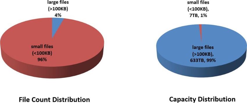
© 2021 Dell Inc. or its subsidiaries.Improvement of Runtimes for Concurrent Jobs For a semiconductor design workflow, PowerScale scale-out distributed architecture eliminates CPU bottlenecks and optimizes the performance of processing concurrent jobs. Because all the nodes work in parallel, OneFS automatically distributes jobs with SmartConnect to each node instead of running all the jobs against a single controller or requiring the manual distribution of jobs to controllers. With the right number of nodes, the cluster can process concurrent I/O requests from the compute grid with the optimal level of performance. The distributed, parallel architecture of cluster can reduce wall clock runtime for concurrent jobs after the time that other traditional storage systems hit a saturation point for the controller. For most workflows, the intensity of I/O operations necessitates solid-state drives (SSDs), write coalescing, coherent caching, and clustered RAM to efficiently serve requests for files and metadata. Isilon F-Series nodes deliver the performance that semiconductor design workflows and workloads demand. A single F800 All-Flash chassis, in 4U, can supply 250,000 SPECsfs2008 file operations per second with more than 15GB/s of aggregated throughput. A fully scaled cluster can supply up to 9 million NFS SPECsfs2008 file operations per second with more than 540 GB/s of aggregate throughput. The Isilon F800/F810 node combines SSDs with two 16-core Intel CPUs, and up to 36.8 TB of globally coherent cache. SSDs accelerate namespace-intensive metadata operations and access to latency-sensitive data sets. For smaller workloads, the nodes in the Isilon H-Series can also include SSDs to cost-effectively improve performance. PowerScale F200 provides the performance of flash storage in a cost-effective form factor to address the needs of a wide variety of workloads. With new NVMe drives, the PowerScale F600 provides larger capacity with massive performance in a cost-effective compact form factor to power the most demanding workloads. To help eliminate bottlenecks, OneFS includes several cache types, a prefetching option, and dual 40 gigabit Ethernet (40GbE) connections per node. The globally coherent cache provides rapid access to stored data by connecting to any node. You can easily scale the coherent cache to hold your working data set in memory as the data set grows by adding more nodes. The prefetching option can tune OneFS to address streaming, random, or concurrent access patterns. The dual 40 GbE connections to each node support the high levels of network utilization that take place during a semiconductor chip’s simulation and verification phases. Finding aa cluster’s optimal point—the point at which it scales in processing concurrent jobs and reduces wall clock runtimes in relation to other systems for the same workload—depends on the size of your compute grid, the number of jobs, the working data sets, and other factors. We recommend that you work with a Dell EMC Unstructured Data Solutions (UDS) representative to determine the number of nodes that will best serve your workflow. Storage Efficiency and Utilization A typical semiconductor design data set consists of about 90 percent or more small files and 10 percent or less large files stored in a file system of thousands of project directories. About 60 percent of the data is active; 40 percent is inactive. Snapshots usually back up the data for short-term retention combined with a long-term backup strategy, which typically includes disk-to-disk backups or tapes. With traditional filers, a semiconductor design workload utilizes disk space inefficiently. Capacity becomes unevenly distributed across volumes. Of the raw total storage capacity, about 65 percent is usable because of the overhead for parity, spares, snapshot reserve space, the uneven distribution of data, and padding for performance. In practice, overhead often consumes 50 percent of the total capacity because many of the file systems contain pockets of empty space. Our scale-out storage cluster eliminates much of the overhead that traditional semiconductor design storage systems require. By not having RAID groups, OneFS evenly distributes, or stripes, data among a cluster’s nodes with layout algorithms that maximize storage efficiency and performance. The system continuously reallocates data to conserve space. At the same time, OneFS protects data with forward error correction, or FEC—a highly efficient method of reliably protecting data. The capacity overhead for data protection is about 20 percent in aggregate, not per individual volume. In practice, a PowerScale cluster runs at between 70 and 80 percent efficiency for a semiconductor design data set because it is the large files that dominate utilization, saving as much as 20 to 30 percent of capacity over traditional storage systems. Even when small files make up more than 90 percent of a semiconductor design data set, they consume only 10 percent or less of the capacity. As such, any inefficiencies in storing small files are overshadowed by the efficiencies in storing large files. And as a semiconductor design data set increases in size, our cluster moves closer to 80 percent efficiency. © 2021 Dell Inc. or its subsidiaries.
Furthermore, in the file count vs. capacity distribution scenario shown in the following chart, the level of efficiency is
79 percent:

                                  Figure 2: Large Files vs Small Files by count and capacity

In addition, you can non-disruptively expand the capacity of the cluster by monitoring the used space on its single
volume and then adding nodes just in time to address requirements for more capacity. As a result, semiconductor design
system administrators can extract much higher utilization rates from the storage system without risking excessive
downtime and without imperiling performance.

Project directories that are spread across volumes—there can be anywhere from tens to hundreds of directories in a
volume and up to thousands of directories spread across multiple controllers—find a convenient home on our scale-out
cluster. OneFS automatically balances data across the entire cluster. As a result, a cluster can be oversubscribed for
semiconductor design storage, and you can expand the cluster non-disruptively to meet expanding storage
requirements just in time.

Automated tiering further increases storage efficiency. With other storage systems, moving inactive data to a lower tier can
require significant manual effort. With OneFS, a policy can automatically move inactive data to a lower storage tier. As
much as 40 percent of semiconductor design file sets can be inactive for 120 days. Automated tiering with OneFS can
save more than a third of the money spent on tier 1 storage. Snapshots can also reside on a lower tier; there is no need to
set aside snapshot reserve space.

Data Management

A PowerScale cluster simplifies data management to reduce operating expenses. PowerScale’s unique scale-out
approach ensures a high return on investment through efficient management while seamlessly scaling to match the
ever-increasing storage requirements for semiconductor design project data. Specifically, a PowerScale cluster
solves many common data management problems for semiconductor companies by providing capabilities that
traditional storage systems lack.

A Single Volume

A cluster presents all the nodes in a cluster as a single, global namespace with a central point of management.
Semiconductor compute clients access the same data by connecting to any node. No storage silos muddle data
management.

Seamless Scalability

PowerScale OneFS enables semiconductor companies to scale performance and capacity based on the requirements
of their business. With up to 252 nodes in a cluster, they can scale capacity to 10s of petabytes of storage and
scale performance up to 15.8 million file operations per second with up to 945 gigabytes per second of aggregate
throughput - non-disruptively.

© 2021 Dell Inc. or its subsidiaries.
Efficient Data Management Traditional scale-up architectures can result in costly, manual data migrations among components to balance performance for applications. A PowerScale cluster evenly distributes data among nodes or within storage pools without leaving hot spots. The hot spots are inherently eliminated by the file system’s scale-out, distributed architecture. There is no need to manually migrate data. With a single volume, a cluster requires no manual reconfiguration of client mount points. Service-level agreements become predictable. A cluster can combine nodes of different types into a single file system and then segment them into storage pools with different capacity-to-performance ratios. PowerScale SmartPools can, for example, implement file pools that maximize performance for working data sets while cost-effectively storing only active data on all flash tier and warm and cold data to hybrid and cold tiers. File pool policies can identify different data sets by age and then distribute them to a storage tier that matches their performance requirements. Technology Strategy By scaling multidimensionally to handle the exponential growth of semiconductor design data, a PowerScale cluster provides the best of both worlds: capacity and performance. The combination helps you adapt to fluid storage requirements, non-disruptively add capacity and performance in cost-effective increments, and improve wall-clock run times for concurrent jobs. For semiconductor design workloads, the ratio of CPU, RAM, and disk space depends on the workload - factors that make it difficult to size a storage system before you can measure a future project’s workload. Expanding data sets also makes upfront sizing decisions problematic. PowerScale scale-out NAS lends itself perfectly to this scenario: You can increase CPUs, RAM, and disk space by adding nodes to match storage capacity and performance with the demands of a dynamic and challenging semiconductor design workload. PowerScale gives you the agility to adapt to changing storage requirements. Instead of purchasing a new fully scaled controller, you can non-disruptively add nodes in cost-effective increments to expand performance, capacity, or both. As part of a technology strategy to shorten a chip’s time to market, a correctly sized PowerScale cluster can reduce the wall clock runtime for concurrent jobs after the time that other storage systems hit a saturation point for the controller. Being able to run more concurrent jobs without saturating the storage system shortens the time it takes to design and build a chip, which can in turn help improve revenue and profit margins. 4. Conclusion Powered by OneFS, Dell EMC PowerScale overcomes the problems that undermine traditional NAS systems by combining the three traditional layers of storage architecture - file system, volume manager, and data protection - into a scale-out NAS cluster with a distributed file system. For semiconductor companies, PowerScale eliminates controller bottlenecks to reduce wall-clock runtimes for concurrent jobs, accelerates metadata operations, improves storage efficiency to lower capital expenditures, centralizes management to reduce operating expenses, and delivers strategic advantages to reduce a chip’s time to market. © 2021 Dell Inc. or its subsidiaries. All Rights Reserved. Dell Technologies, Dell, EMC and other trademarks are trademarks of Dell Inc. or its subsidiaries. Other trademarks may be trademarks of their respective owners. Reference Number: H13233.3
You can also read