SysCLOCK PLL Design and Usage Guide for Nexus Platform Technical Note - FPGA-TN-02095-1.6
←
→
Page content transcription
If your browser does not render page correctly, please read the page content below
sysCLOCK PLL Design and Usage Guide for
Nexus Platform

Technical Note

FPGA-TN-02095-1.6

September 2021
sysCLOCK PLL Design and Usage Guide for Nexus Platform
Technical Note

Disclaimers
Lattice makes no warranty, representation, or guarantee regarding the accuracy of information contained in this document or the suitability of its
products for any particular purpose. All information herein is provided AS IS and with all faults, and all risk associated with such information is entirely
with Buyer. Buyer shall not rely on any data and performance specifications or parameters provided herein. Products sold by Lattice have been
subject to limited testing and it is the Buyer's responsibility to independently determine the suitability of any products and to test and verify the
same. No Lattice products should be used in conjunction with mission- or safety-critical or any other application in which the failure of Lattice’s
product could create a situation where personal injury, death, severe property or environmental damage may occur. The information provided in this
document is proprietary to Lattice Semiconductor, and Lattice reserves the right to make any changes to the information in this document or to any
products at any time without notice.

 © 2019-2021 Lattice Semiconductor Corp. All Lattice trademarks, registered trademarks, patents, and disclaimers are as listed at www.latticesemi.com/legal.
 All other brand or product names are trademarks or registered trademarks of their respective holders. The specifications and information herein are subject to change without notice.

2 FPGA-TN-02095-1.6
sysCLOCK PLL Design and Usage Guide for Nexus Platform
 Technical Note

Contents
Acronyms in This Document ................................................................................................................................................. 7
1. Introduction .................................................................................................................................................................. 8
2. Clock/Control Distribution Network ............................................................................................................................. 8
3. Nexus Top-Level View ................................................................................................................................................... 9
4. Clocking Architecture Overview ................................................................................................................................. 11
 4.1. Primary Clock Network...................................................................................................................................... 11
 4.2. Edge Clock Network .......................................................................................................................................... 11
5. Overview of Clocking Components ............................................................................................................................. 12
 5.1. Edge Clock Dividers (ECLKDIV) .......................................................................................................................... 12
 5.2. Primary Clock Divider (PCLKDIV) ....................................................................................................................... 12
 5.3. Dynamic Clock Select (DCS) ............................................................................................................................... 12
 5.4. Dynamic Clock Control (DCC) ............................................................................................................................ 12
 5.5. Edge Clock Sync (ECLKSYNC) ............................................................................................................................. 12
 5.6. Oscillator (OSC) ................................................................................................................................................. 12
6. Primary Clocks ............................................................................................................................................................ 13
 6.1. Primary Clock Sources ....................................................................................................................................... 13
 6.2. Primary Clock Routing ....................................................................................................................................... 13
 6.3. Dedicated Clock Inputs...................................................................................................................................... 14
7. Primary Clock Divider (PCLKDIV)................................................................................................................................. 15
 7.1. PCLKDIV Component Definition ........................................................................................................................ 15
 7.2. PCLKDIV Usage in VHDL..................................................................................................................................... 16
 7.3. PCLKDIV Usage in Verilog .................................................................................................................................. 16
8. Dynamic Clock Select (DCS) ........................................................................................................................................ 17
 8.1. DCS Timing Diagrams ........................................................................................................................................ 18
 8.1.1. Functionality – posedge SEL switch .............................................................................................................. 18
 8.1.2. Functionality – negedge SEL switch ............................................................................................................. 19
 8.1.3. Functionality – bypass .................................................................................................................................. 19
 8.2. DCS Component Definition ............................................................................................................................... 20
 8.3. DCS Usage in VHDL ............................................................................................................................................ 21
 8.4. DCS Usage in Verilog ......................................................................................................................................... 21
9. Dynamic Clock Control (DCC) ...................................................................................................................................... 23
 9.1. Component Definition ....................................................................................................................................... 24
 9.2. DCC Usage in VHDL ........................................................................................................................................... 24
 9.3. DCC Usage in Verilog ......................................................................................................................................... 25
10. Internal Oscillator (OSCA) ........................................................................................................................................... 26
 10.1. OSCA Component Definition ............................................................................................................................. 26
 10.2. OSCA Usage in VHDL ......................................................................................................................................... 27
 10.3. OSCA Usage in Verilog ....................................................................................................................................... 28
11. Edge Clocks ................................................................................................................................................................. 29
 11.1. Edge Clock Dividers (ECLKDIV) .......................................................................................................................... 29
 11.2. ECLKDIV Component Definition ........................................................................................................................ 29
 11.3. ECLKDIV Usage in VHDL ..................................................................................................................................... 30
 11.4. ECLKDIV Usage in Verilog .................................................................................................................................. 31
12. Edge Clock Synchronization (ECLKSYNC) .................................................................................................................... 32
 12.1. ECLKSYNC Component Definition ..................................................................................................................... 32
 12.2. ECLKSYNC Usage in VHDL .................................................................................................................................. 33
 12.3. ECLKSYNC Usage in Verilog ............................................................................................................................... 33
13. General Routing for Clocks ......................................................................................................................................... 34
14. sysCLOCK PLL .............................................................................................................................................................. 35
 14.1. sysCLOCK PLL Overview..................................................................................................................................... 35
 14.2. PLL Features ...................................................................................................................................................... 36
 14.2.1. Dedicated PLL Inputs .................................................................................................................................... 36

 © 2019-2021 Lattice Semiconductor Corp. All Lattice trademarks, registered trademarks, patents, and disclaimers are as listed at www.latticesemi.com/legal.
 All other brand or product names are trademarks or registered trademarks of their respective holders. The specifications and information herein are subject to change without notice.

FPGA-TN-02095-1.6 3
sysCLOCK PLL Design and Usage Guide for Nexus Platform
Technical Note

 14.2.2. Clock Injection Delay Removal .....................................................................................................................37
 14.2.3. Clock Phase Adjustment ...............................................................................................................................37
 14.2.4. Frequency Synthesis .....................................................................................................................................37
 14.2.5. Legacy Mode (Standby) ................................................................................................................................37
 14.3. sysCLOCK PLL Component Definition ................................................................................................................ 37
 14.4. Functional Description ...................................................................................................................................... 39
 14.4.1. Refclk (CLKI) Divider......................................................................................................................................39
 14.4.2. Feedback Loop (CLKFB) Divider ....................................................................................................................39
 14.4.3. Output Clock Dividers (CLKOP, CLKOS, CLKOS2, CLKOS3, CLKOS4, CLKOS5) ................................................40
 14.4.4. Phase Adjustment (Static Mode) ..................................................................................................................40
 14.4.5. Phase Adjustment (Dynamic Mode) .............................................................................................................40
 14.5. PLL Inputs and Outputs ..................................................................................................................................... 40
 14.5.1. CLKI Input .....................................................................................................................................................40
 14.5.2. CLKFB Input ..................................................................................................................................................40
 14.5.3. RST Input ......................................................................................................................................................40
 14.5.4. Dynamic Clock Enables .................................................................................................................................41
 14.5.5. PLLPD_EN_N Input .......................................................................................................................................41
 14.5.6. Dynamic Phase Shift Inputs ..........................................................................................................................41
 14.5.7. PHASESEL Input ............................................................................................................................................41
 14.5.8. PHASEDIR Input ............................................................................................................................................42
 14.5.9. PHASESTEP Input ..........................................................................................................................................42
 14.5.10. PHASELOADREG Input ..................................................................................................................................42
 14.5.11. PLL Clock Outputs .........................................................................................................................................43
 14.5.12. LOCK Output .................................................................................................................................................43
 14.6. Dynamic Phase Adjustment .............................................................................................................................. 43
 14.6.1. VCO Phase Shift ............................................................................................................................................43
 14.6.2. Divider Phase Shift ........................................................................................................................................44
 14.6.3. Total Phase Shift ...........................................................................................................................................45
 14.7. Fractional-N Synthesis Operation...................................................................................................................... 45
 14.8. Spread Spectrum Clock Generation .................................................................................................................. 45
 14.9. Low Power Features .......................................................................................................................................... 47
 14.9.1. Dynamic Clock Enable...................................................................................................................................47
 14.10. PLL Usage in IP Catalog ...................................................................................................................................... 47
 14.10.1. Configuration Tab .........................................................................................................................................48
 14.10.2. PLL Frequency and Phase Configuration ......................................................................................................48
Appendix A. Primary Clock Sources and Distribution ................................................................................................... 54
Appendix B. Pinout Rules for Clocking in Nexus Devices .............................................................................................. 58
Appendix C. PLL LMMI Operation ................................................................................................................................. 59
 PLL Architecture .............................................................................................................................................................. 59
 LMMI Register Map ........................................................................................................................................................ 59
Technical Support Assistance ............................................................................................................................................. 68
Revision History .................................................................................................................................................................. 69

 © 2019-2021 Lattice Semiconductor Corp. All Lattice trademarks, registered trademarks, patents, and disclaimers are as listed at www.latticesemi.com/legal.
 All other brand or product names are trademarks or registered trademarks of their respective holders. The specifications and information herein are subject to change without notice.

4 FPGA-TN-02095-1.6
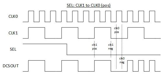
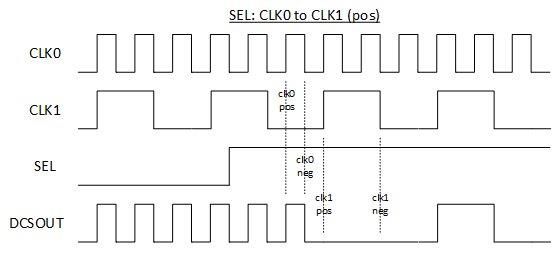
sysCLOCK PLL Design and Usage Guide for Nexus Platform
 Technical Note

Figures
Figure 3.1. CrossLink-NX and Certus-NX Clocking Structure ................................................................................................. 9
Figure 3.2. CertusPro-NX Clocking Structure ...................................................................................................................... 10
Figure 6.1. Primary Clock Routing Architecture for CrossLink-NX and Certus-NX .............................................................. 13
Figure 6.2. Primary Clock Routing Architecture for CertusPro-NX ..................................................................................... 14
Figure 7.1. PCLKDIV Component Symbol ............................................................................................................................ 15
Figure 8.1. DCS_CMUX Structure for CrossLink-NX and Certus-NX .................................................................................... 17
Figure 8.2. DCS_CMUX Structure for CertusPro-NX ........................................................................................................... 17
Figure 8.3. DCS Logic Structure ........................................................................................................................................... 18
Figure 8.4. Posedge DCS Switch from SEL: 0 => 1 ............................................................................................................... 18
Figure 8.5. Posedge DCS Switch from SEL: 1 => 0 ............................................................................................................... 19
Figure 8.6. Negedge DCS Switch from SEL: 0 => 1 .............................................................................................................. 19
Figure 8.7. SELFORCE = 1 DCS Clock Switch ........................................................................................................................ 20
Figure 8.8. DCS Component Symbol ................................................................................................................................... 20
Figure 9.1. Glitchless DCC Functional Waveform ............................................................................................................... 23
Figure 9.2. DCC Component Symbol ................................................................................................................................... 24
Figure 10.1. OSCA Component Symbol............................................................................................................................... 26
Figure 11.1. Edge Clock Sources Per Bank .......................................................................................................................... 29
Figure 11.2. ECLKDIV Component Symbol .......................................................................................................................... 30
Figure 12.1. ECLKSYNC Component Symbol ....................................................................................................................... 32
Figure 12.2. ECLKSYNC Functional Waveform .................................................................................................................... 33
Figure 13.1. Gated Clock to the Primary Clock Routing ...................................................................................................... 34
Figure 13.2. Gated Clock to Small Logic Domain ................................................................................................................ 34
Figure 14.1. Nexus PLL Block Diagram ................................................................................................................................ 35
Figure 14.2. PLL Input Pins for LIFCL-40 and LFD2NX-40 .................................................................................................... 36
Figure 14.3. PLL Input Pins for LIFCL-17 and LFD2NX-17 .................................................................................................... 36
Figure 14.4. PLL Input Pins for LFCPNX-50 .......................................................................................................................... 36
Figure 14.5. PLL Input Pins for LFCPNX-100 ........................................................................................................................ 36
Figure 14.6. PLL Component Instance ................................................................................................................................ 38
Figure 14.7. RST Input Timing Diagram .............................................................................................................................. 41
Figure 14.8. PLL Phase Shifting Using the PHASESTEP Signal ............................................................................................. 44
Figure 14.9. Divider Phase Shift Timing Diagram ................................................................................................................ 44
Figure 14.10. Center Spread Profile .................................................................................................................................... 46
Figure 14.11. Down Spread Profile ..................................................................................................................................... 46
Figure 14.12. Dynamic Clock Enable for PLL Outputs ......................................................................................................... 47
Figure 14.13. IP Catalog Main Window for PLL Module ..................................................................................................... 48
Figure 14.14. Nexus PLL Frequency Configuration in General Tab ..................................................................................... 49
Figure 14.15. Nexus PLL Optional Ports Configuration Tab ................................................................................................ 52
Figure A.1. Nexus Primary Clock Sources and Distribution, LIFCL-40 and LFD2NX-40 Devices .......................................... 54
Figure A.2. Nexus Primary Clock Sources and Distribution, LIFCL-17 and LFD2NX-17 Devices .......................................... 55
Figure A.3. Nexus Primary Clock Sources and Distribution, LFCPNX-50 Devices ................................................................ 56
Figure A.4. Nexus Primary Clock Sources and Distribution, LFCPNX-100 Devices .............................................................. 57

 © 2019-2021 Lattice Semiconductor Corp. All Lattice trademarks, registered trademarks, patents, and disclaimers are as listed at www.latticesemi.com/legal.
 All other brand or product names are trademarks or registered trademarks of their respective holders. The specifications and information herein are subject to change without notice.

FPGA-TN-02095-1.6 5
sysCLOCK PLL Design and Usage Guide for Nexus Platform
Technical Note

Tables
Table 1.1. Number of PLLs, Edge Clocks, and Clock Dividers ................................................................................................8
Table 7.1. PCLKDIV Component Port Definition .................................................................................................................15
Table 7.2. PCLKDIV Component Attribute Definition .........................................................................................................15
Table 8.1. DCS Component Port Definition .........................................................................................................................20
Table 8.2. DCS – DCSMODE Attribute .................................................................................................................................21
Table 9.1. DCC Component Port Definition ........................................................................................................................24
Table 10.1. OSCA Component Port Definition ....................................................................................................................26
Table 10.2. OSCA Component Attribute Definition ............................................................................................................27
Table 11.1. ECLKDIV Component Port Definition ...............................................................................................................30
Table 11.2. ECLKDIV Component Attribute Definition ........................................................................................................30
Table 12.1. ECLKSYNC Component Port Definition .............................................................................................................32
Table 12.2. ECLKSYNC Component Attribute Definition .....................................................................................................32
Table 14.1. PLL Component Port Definition........................................................................................................................39
Table 14.2. PLL Clock Output Enable Signal List ..................................................................................................................41
Table 14.3. PHASESEL Signal Settings Definition ................................................................................................................42
Table 14.4. PHASEDIR Signal Settings Definition ................................................................................................................42
Table 14.5. PLL Clock Outputs and ECLK Connectivity ........................................................................................................43
Table 14.6. Tab 1, General Settings, IP Catalog User Interface...........................................................................................50
Table 14.7. Tab 2, PLL Optional Ports, IP Catalog User Interface .......................................................................................52
Table B.1. Clock Input Selection Table ................................................................................................................................58
Table C.1. PLL Data Bus Port Definition ..............................................................................................................................59
Table C.2. LMMI Offset Address Locations for PLL Registers ..............................................................................................59
Table C.3. PLL Registers Descriptions .................................................................................................................................61

 © 2019-2021 Lattice Semiconductor Corp. All Lattice trademarks, registered trademarks, patents, and disclaimers are as listed at www.latticesemi.com/legal.
 All other brand or product names are trademarks or registered trademarks of their respective holders. The specifications and information herein are subject to change without notice.

6 FPGA-TN-02095-1.6
sysCLOCK PLL Design and Usage Guide for Nexus Platform
 Technical Note

Acronyms in This Document
A list of acronyms used in this document.
 Acronym Definition
 CIB Common Interface Block
 DCC Dynamic Clock Control
 DCS Dynamic Clock Select
 DDR Double Data Rate
 DLL Delay Locked Loop
 DTR Digital Temperature Readout
 GSR Global Set Reset
 LMMI Lattice Memory Mapped Interface
 MIB Memory Interface Block
 PLC Programmable Logic Cell
 PLL Phase Locked Loop
 SED Soft Error Detect

 © 2019-2021 Lattice Semiconductor Corp. All Lattice trademarks, registered trademarks, patents, and disclaimers are as listed at www.latticesemi.com/legal.
 All other brand or product names are trademarks or registered trademarks of their respective holders. The specifications and information herein are subject to change without notice.

FPGA-TN-02095-1.6 7
sysCLOCK PLL Design and Usage Guide for Nexus Platform
Technical Note

1. Introduction
This usage guide describes the clock resources available in the Lattice Nexus™ Platform architecture, which includes
CrossLink™-NX, Certus™-NX, and CertusPro™-NX product families.
The details are provided for Primary Clocks, Edge Clocks, PLLs, the Internal Oscillator, and clocking elements such as
Clock Dividers, Clock Multiplexers, and Clock Stop Blocks available in the Nexus device.
The number of PLLs, Edge Clocks, and Clock Dividers for each device is listed in Table 1.1.
Table 1.1. Number of PLLs, Edge Clocks, and Clock Dividers
 LIFCL-40 LIFCL-17
Parameter Description LFCPNX-50 LFCPNX-100
 LFD2NX-40 LFD2NX-17
Number of PLLs General purpose Phase Locked Loops. 3 2 3 4
Number of Edge
 Edge Clocks for high-speed interfaces. 12 12 12 12
Clocks
Number of Edge
 Edge Clock Dividers for high-speed interfaces. 12 12 12 12
Clock Dividers
Number of
 Programmable Primary Clock dividers for domain
Primary Clock 1 1 2 2
 crossing applications.
Dividers
Number of DDRDLL used for DDR memory and High Speed I/O
 2 2 2 2
DDRDLLs interfaces

It is very important to validate the device pinout using the Lattice Radiant™ tool to avoid implementation issues.

2. Clock/Control Distribution Network
Nexus devices provide global clock distribution in the form of global primary clocks. The device is organized into clock
regions; each clock region can accommodate 16 primary clocks. For CrossLink-NX and Certus-NX, there are two clock
regions and for CertusPro-NX there are four clock regions. There is a maximum of 64 unique clock input sources. The
Nexus primary clocking structure is Edge Clock rich and contains generous low-skew Primary clock resources.

 © 2019-2021 Lattice Semiconductor Corp. All Lattice trademarks, registered trademarks, patents, and disclaimers are as listed at www.latticesemi.com/legal.
 All other brand or product names are trademarks or registered trademarks of their respective holders. The specifications and information herein are subject to change without notice.

8 FPGA-TN-02095-1.6
sysCLOCK PLL Design and Usage Guide for Nexus Platform
 Technical Note

3. Nexus Top-Level View
A top-level view of the major clocking resources for the CrossLink-NX and Certus-NX devices is shown in Figure 3.1. The
shaded blocks (PCIe®, upper left PLL, and I/O Bank 2/Bank 6/Bank 7) are not available in the LIFCL-17 and LFD2NX-17
devices. The MIPI_DPHY0 and MIPI_DPHY1 on the top are only available for the CrossLink-NX family.

 PCIe

 PLL MIPI_DPHY0 MIPI_DPHY1 BANK 0 PCLK OSC

 6 2 2 2 2

 Top MIDMUX

 BANK 1 PCLK
 BANK 7 PCLK

 16 DCC
 3

 3
 16 Primary Sources
 Primary Clocks Primary Clocks
 For Left Clock Region For Right Clock Region
 16 Fabric Fabric 16
 Entry Entry

 Right MIDMUX
 Left MIDMUX

 12 12 Primary Sources 12 Primary Sources 12
 12 DCC DCS DCS 12 DCC
 MUX MUX

 Fabric Fabric
 Entry Entry

 BANK 2 PCLK
 BANK 6 PCLK

 18 Primary Sources
 3

 18 DCC

 3
 Bottom MIDMUX

 6 4 4 6
 4 4 4 4

 PLL BANK 5 PCLK ECLK BANK 4 PCLK ECLK BANK 3 PCLK ECLK PLL

 Figure 3.1. CrossLink-NX and Certus-NX Clocking Structure

A top-level view of the major clocking resources for the CertusPro-NX devices is shown in Figure 3.2. The Upper Right
PLL is only for LFCPNX-100.

 © 2019-2021 Lattice Semiconductor Corp. All Lattice trademarks, registered trademarks, patents, and disclaimers are as listed at www.latticesemi.com/legal.
 All other brand or product names are trademarks or registered trademarks of their respective holders. The specifications and information herein are subject to change without notice.

FPGA-TN-02095-1.6 9
sysCLOCK PLL Design and Usage Guide for Nexus Platform
Technical Note

 PLL SerDes BANK 0 PCLK OSC PLL

 TMID

 BANK 1 PCLK
 16 DCC

 RMID
 LMID

 12 DCC

 BANK 2 PCLK
 18 DCC

 BMID

 PLL BANK 5 PCLK ECLK BANK 4 PCLK ECLK BANK 3 PCLK ECLK PLL

 Figure 3.2. CertusPro-NX Clocking Structure

 © 2019-2021 Lattice Semiconductor Corp. All Lattice trademarks, registered trademarks, patents, and disclaimers are as listed at www.latticesemi.com/legal.
 All other brand or product names are trademarks or registered trademarks of their respective holders. The specifications and information herein are subject to change without notice.

10 FPGA-TN-02095-1.6
sysCLOCK PLL Design and Usage Guide for Nexus Platform
 Technical Note

4. Clocking Architecture Overview
Below is a brief overview of the clocking structure, elements, and PLL. Greater detail is provided starting with the
Appendix A. Primary Clock Sources and Distribution and Appendix B Pinout Rules for Clocking in Nexus Devices section.

4.1. Primary Clock Network
Up to 32 primary clocks (for CrossLink-NX and Certus-NX) or 64 primary clocks (for CertusPro-NX) can be selected from
up to 64 Primary Clock Sources (PLLs, External Inputs, SERDES, and others) and routed to the Primary Clock Network.
The Primary Clock Network provides low-skew, high fan-out clock distribution to all synchronous elements in the FPGA
fabric. The Primary Clock Network is divided into two clocking regions (for CrossLink-NX and Certus-NX) or four clocking
regions (for CertusPro-NX), each region associated with a DCS_CMUX. Each of these regions has 16 clocks that can be
distributed to the fabric in the region. Initially, the Lattice Radiant software automatically routes each clock region; up
to a maximum of 16 clocks. You can change how the clocks are routed by specifying a preference in the Lattice Radiant
project constraints file to locate the clock to specific region.

4.2. Edge Clock Network
Edge Clocks are low skew, high speed clock resources used to clock data into/out of the I/O logic of Nexus devices.
There are four Edge Clocks per bank located on the bottom side of the device.

 © 2019-2021 Lattice Semiconductor Corp. All Lattice trademarks, registered trademarks, patents, and disclaimers are as listed at www.latticesemi.com/legal.
 All other brand or product names are trademarks or registered trademarks of their respective holders. The specifications and information herein are subject to change without notice.

FPGA-TN-02095-1.6 11
sysCLOCK PLL Design and Usage Guide for Nexus Platform
Technical Note

5. Overview of Clocking Components

5.1. Edge Clock Dividers (ECLKDIV)
Edge Clock dividers are provided to create the divided down clocks used for the I/O Mux/DeMux gearing logic (SCLK
inputs of DDR I/O) and they drive the Primary Clock network. There are twelve Edge Clock Dividers on the Nexus
device.

5.2. Primary Clock Divider (PCLKDIV)
For CrossLink-NX and Certus-NX, one programmable Primary Clock Divider is provided to create the divided down
clocks. For CertusPro-NX, two programmable Primary Clock Dividers are available.

5.3. Dynamic Clock Select (DCS)
The dynamic clock select provides run-time selectable glitchless or non-glitchless operation between two independent
clock sources to the primary clock network. This clock select allows the selection of clock sources without leaving the
dedicated clock resources in the device. There is one dynamic clock select block on the CrossLink-NX and Certus-NX
devices, and there are two dynamic clock select blocks on the CertusPro-NX device.

5.4. Dynamic Clock Control (DCC)
Dynamic Clock Control allows dynamic clock enable and disables the MIDMUX Feed Line and the four special common
interface block (CIB) clocks from the core. When a Feed Line is disabled, all the logic and clock signals that are fed by
this Feed Line do not toggle. Hence, it reduces the overall dynamic power consumption of the device.

5.5. Edge Clock Sync (ECLKSYNC)
The Nexus devices have dynamic edge clock synchronization control (ECLKSYNC) which allows each edge clock to be
disabled or enabled glitchlessly from core logic if desired. This allows you to synchronize the edge clock to an event or
external signal, if desired. It also allows the design to dynamically disable a clock and its associated logic in the design
when it is not needed and thus save power.

5.6. Oscillator (OSC)
An internal programmable rate oscillator is provided. The oscillator can be used for FPGA configuration, Soft Error
Detect (SED), and as a user logic clock source that is available after FPGA configuration. There is one OSCA on the Nexus
device. The oscillator clock output is routed directly to primary clocking.
The oscillator output is not a high-accuracy clock, having a +/- 15% variation in its output frequency. It is mainly used
for circuits that do not require a high degree of clock accuracy. Examples of usage are asynchronous logic blocks such
as a timer or reset generator, or other logic that require a constantly running clock.

 © 2019-2021 Lattice Semiconductor Corp. All Lattice trademarks, registered trademarks, patents, and disclaimers are as listed at www.latticesemi.com/legal.
 All other brand or product names are trademarks or registered trademarks of their respective holders. The specifications and information herein are subject to change without notice.

12 FPGA-TN-02095-1.6
sysCLOCK PLL Design and Usage Guide for Nexus Platform
 Technical Note

6. Primary Clocks

6.1. Primary Clock Sources
The primary clock network has multiple inputs, called primary clock sources, which can be routed directly to the
primary clock routing to clock the FPGA fabric.
The primary clock sources that can connect to the primary clock routing are:
 Dedicated Clock Input Pins
 PLL Outputs
 PCLKDIV/ECLKDIV Outputs
 Internal FPGA Fabric Entries (with minimum general routing)
 SGMII-CDR, SERDES/PCS clocks
 OSC Clock
All potential primary clock sources are multiplexed prior to going to the primary clock routing by a MIDMUX. There are
58 MIDMUX connections and four FPGA fabric connections, 62 total, routed to a multiplexor in the center of the chip
called the centermux. From the centermux, primary clocks are selected and distributed to the FPGA fabric.
The maximum number of unique clock sources is:
18 bottom MIDMUX sources + 16 top MIDMUX sources + 12 left MIDMUX sources + 12 right MIDMUX sources + 4
direct FPGA fabric entry points (from general routing) = 62.
The basic clocking structure is shown in Figure 3.1 and Figure 3.2, elaborated in Appendix A. Primary Clock Sources and
Distribution.

6.2. Primary Clock Routing
The primary clock routing network is made up of low skew clock routing resources with connectivity to every
synchronous element of the device. Primary clock sources are selected at the MIDMUX, then selected in the centermux
and distributed on the primary clock routing to clock the synchronous elements in the FPGA fabric. For CrossLink-NX
and Certus-NX, the primary clock routing network is divided into left and right regions. Figure 6.1 is the simplified view
of Figure 3.1. For CertusPro-NX, the primary clock routing network is divided into four regions, up-left, up-right, low-
left, and low-right. Figure 6.2 is the simplified view of Figure 3.2.

 MID
 MUX

 MID MID
 MUX MUX

 MID
 MUX

 Figure 6.1. Primary Clock Routing Architecture for CrossLink-NX and Certus-NX

 © 2019-2021 Lattice Semiconductor Corp. All Lattice trademarks, registered trademarks, patents, and disclaimers are as listed at www.latticesemi.com/legal.
 All other brand or product names are trademarks or registered trademarks of their respective holders. The specifications and information herein are subject to change without notice.

FPGA-TN-02095-1.6 13
sysCLOCK PLL Design and Usage Guide for Nexus Platform
Technical Note

 MID
 MUX

 MID MID
 MUX MUX

 MID
 MUX

 Figure 6.2. Primary Clock Routing Architecture for CertusPro-NX

The centermux can source up to 16 independent primary clocks per region, which can clock the logic located in that
region. The centermux can also route each clock source to all regions. The Lattice Radiant software automatically
routes a primary clock to the regions in the FPGA.

6.3. Dedicated Clock Inputs
The Nexus device has dedicated pins, called PCLK pins, to bring an external clock source into the FPGA and allow them
to be used as FPGA primary clocks. These inputs route directly to the Primary clock network, and to Edge Clock routing
resources. A dedicated PCLK clock pin must always be used to route an external clock source to FPGA and I/O logic.
If an external input clock is being sourced to a PLL, then in most cases, the input clock should use a dedicated PLL input
pin as described in Dedicated PLL Inputs section. SERDES reference clocks also have dedicated SERDES reference clock
pins. The Nexus device allows a PLL reference clock or a SERDES reference clock to come from an external Primary
Clock (PCLK) pin and route through the Primary clock network to drive the reference clock to the SERDES or the input of
a PLL. See Appendix A for more details.

 © 2019-2021 Lattice Semiconductor Corp. All Lattice trademarks, registered trademarks, patents, and disclaimers are as listed at www.latticesemi.com/legal.
 All other brand or product names are trademarks or registered trademarks of their respective holders. The specifications and information herein are subject to change without notice.

14 FPGA-TN-02095-1.6
sysCLOCK PLL Design and Usage Guide for Nexus Platform
 Technical Note

7. Primary Clock Divider (PCLKDIV)
Inside the centermux, one (for CrossLink-NX and Certus-NX) or two (for CertusPro-NX) Primary Clock Dividers are
available. Each Primary Clock Divider provides the following functionalities:
 PCLK Divider supports ÷2, ÷4, ÷8, ÷16, ÷32, ÷64, and ÷128. When PCLK divider is bypassed, it is ÷1 mode.
 PCLK Divider can be reset by global Reset signals and sleep mode control signals. The global reset can be disabled
 by a configuration bit.
 PCLK Divider supports user Local Reset through CIB port.
 The reset is Asynchronous assert and synchronous de-assert. The divider output starts at the next cycle after the
 reset is synchronously released.
 Allow GSR activity to be ignored during device power up by gating this signal with internal DONE.
 When exiting from sleep mode, the retention registers are released from the asynchronous reset control.

7.1. PCLKDIV Component Definition
The PCLKDIV component can be instantiated in the source code of a design as defined in this section. Figure 7.1,
Table 7.1, and Table 7.2 define the PCLKDIV component. Verilog and VHDL instantiations are included.

 PCLKDIV

 CLKIN CLKOUT
 LSRPDIV

 Figure 7.1. PCLKDIV Component Symbol

Table 7.1. PCLKDIV Component Port Definition
 Port Name I/O Description
 CLKIN I Primary Clock Input
 Local Reset — Active High, asynchronously forces all outputs low.
 LSRPDIV I LSRPDIV = 0 Clock outputs are active
 LSRPDIV = 1 Clock outputs are OFF
 CLKOUT O Divide by 1, 2, 4, 8, 16, 32, 64, or 128 Output Port

Table 7.2. PCLKDIV Component Attribute Definition
 Name Value Default Description
 X1, X2, X4, X8, X16, X32, X64,
 DIV_PCLKDIV X1 Primary Clock Divide Ratio Selection
 X128
 ENABLE
 GSR ENABLED GSR ENABLE/DISABLE Selection
 DISABLE

 © 2019-2021 Lattice Semiconductor Corp. All Lattice trademarks, registered trademarks, patents, and disclaimers are as listed at www.latticesemi.com/legal.
 All other brand or product names are trademarks or registered trademarks of their respective holders. The specifications and information herein are subject to change without notice.

FPGA-TN-02095-1.6 15
sysCLOCK PLL Design and Usage Guide for Nexus Platform
Technical Note

7.2. PCLKDIV Usage in VHDL
Component Instantiation
Library lattice;
use lattice.components.all;

Component and Attribute Declaration
component PCLKDIV
Generic (DIV_PCLKDIV : string;
 GSR : string);
Port (CLKIN : in STD_LOGIC;
 LSRPDIV : in STD_LOGIC;
 CLKOUT : out STD_LOGIC);
end component;

PCLKDIV Instantiation
attribute DIV_PCLKDIV : string;
attribute DIV_PCLKDIV of I1 : label is “X1”;
attribute GSR : string;
attribute GSR of I1 : label is “DISABLED”;

I1: PCLKDIV
generic map (DIV_PCLKDIV => “2.0”,
 GSR => “DISABLED”)
port map (CLKIN => CLKIN,
 LSRPDIV => LSRPDIV,
 CLKOUT => CLKOUT);

7.3. PCLKDIV Usage in Verilog
Component and Attribute Declaration
module PCLKDIV (CLKIN, LSRPDIV, CLKOUT);

parameter DIV_PCLKDIV = “X2”; // “X1”, “X2”, “X4”, “X8”, “X16”, “X32”, “X64”, “X128”
parameter GSR = “DISABLED”; // “ENABLED”, “DISABLED”

input CLKIN, LSRPDIV;
output CLKOUT;
endmodule

PCLKDIV Instantiation
defparam I1.DIV_PCLKDIV = “X2”;
defparam I1.GSR = “DISABLED”;
PCLKDIV I1 (
 .CLKIN (CLKIN),
 .LSRPDIV (LSRPDIV),
 .CLKOUT (CLKOUT));

 © 2019-2021 Lattice Semiconductor Corp. All Lattice trademarks, registered trademarks, patents, and disclaimers are as listed at www.latticesemi.com/legal.
 All other brand or product names are trademarks or registered trademarks of their respective holders. The specifications and information herein are subject to change without notice.

16 FPGA-TN-02095-1.6
sysCLOCK PLL Design and Usage Guide for Nexus Platform
 Technical Note

8. Dynamic Clock Select (DCS)
One (for CrossLink-NX and Certus-NX) or two (for CertusPro-NX) dynamic clock select (DCS) blocks are located at the
center of the PLC array, which can drive to any or all the regions. The DCS_CMUX Structures are shown in Figure 8.1
and Figure 8.2.

 16 16
 VCCPG Domain

 16x (partial 16x (partial
 (16/64):1) (16/64):1)
 CMUX CMUX
 16 16

 DCS_CMUX dcs2cmux0
 DCS
 62 dcs1 dcs0

 PCLKDIV

 DCMUX DCMUX
 (62:1) (62:1)
 62 62
 62 62

 62

 Figure 8.1. DCS_CMUX Structure for CrossLink-NX and Certus-NX

 16 16 16 16

 16x (partial 16x (partial 16x (partial 16x (partial
 (16/64):1) (16/64):1) (16/64):1) (16/64):1)
 CMUX CMUX CMUX CMUX
 16 16 16 16

 dcs2cmux0 dcs2cmux1
 DCS_CMUX
 DCS DCS

 62 dcs1 dcs0 dcs3 dcs2

 PCLKDIV PCLKDIV

 DCSMUX DCSMUX DCSMUX DCSMUX
 (62:1) (62:1) (62:1) (62:1)
 62 62 62 62
 62 62 62 62

 62

 Figure 8.2. DCS_CMUX Structure for CertusPro-NX

 © 2019-2021 Lattice Semiconductor Corp. All Lattice trademarks, registered trademarks, patents, and disclaimers are as listed at www.latticesemi.com/legal.
 All other brand or product names are trademarks or registered trademarks of their respective holders. The specifications and information herein are subject to change without notice.

FPGA-TN-02095-1.6 17
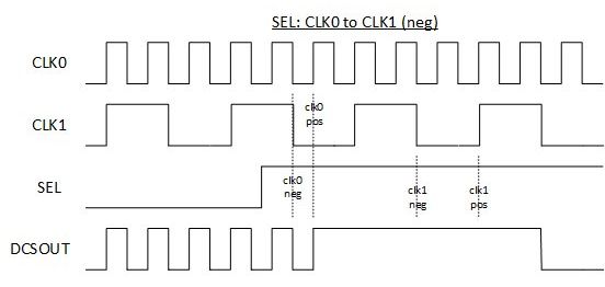
sysCLOCK PLL Design and Usage Guide for Nexus Platform
Technical Note

The DCS block allows dynamic and glitchless selection between two PCLK clock sources. The DCS block shares the same
clock resource as any PCLK CMUX. This way the DCS function can be performed on any two primary clock sources. The
inputs to the DCS block come from all the outputs of MIDMUXs and local routing that is located at the center of the PLC
array. The output of the DCS is connected to the inputs of Primary Clock Center MUXs. The DCS logic structure is shown
in Figure 8.3.

 mc1_dcs
 PCLK Feed 58
 DCS LOGIC

 PCLKDIV
 DCS MUX clk0
 (64:1)
 DCS
 CIBs 4 Logic

 0
 dcs
 1
 PCLK Feed 58
 0

 DCS MUX clk1 1
 (64:1) 0

 CIBs 4
 reset sel sel_force

 Figure 8.3. DCS Logic Structure

The DCSMODE attribute sets the behavior of the DCS output. The DCS attributes are described in Table 8.2.

8.1. DCS Timing Diagrams
The DCS block allows dynamic and glitchless selection between two PCLK clock sources. The DCS block shares the same
clock resource as any PCLK CMUX. Therefore, the DCS function can be performed on any two primary clock sources.
Figure 8.4, Figure 8.5, and Figure 8.6 show the DCS in glitchless operation in conjunction with the DCSMODE attribute.
Figure 8.7 shows the non-glitchless bypass operation scenario.

8.1.1. Functionality – posedge SEL switch
The selection switches from current clock to target clock. For posedge configuration, the latch state is low. Below is the
sequence of events once SEL toggles:
1. Current clock must see posedge then negedge, then is deactivated.
2. Target clock must see posedge then negedge, then output is successfully switched over.

 Figure 8.4. Posedge DCS Switch from SEL: 0 => 1

 © 2019-2021 Lattice Semiconductor Corp. All Lattice trademarks, registered trademarks, patents, and disclaimers are as listed at www.latticesemi.com/legal.
 All other brand or product names are trademarks or registered trademarks of their respective holders. The specifications and information herein are subject to change without notice.

18 FPGA-TN-02095-1.6
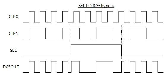
sysCLOCK PLL Design and Usage Guide for Nexus Platform
 Technical Note

 Figure 8.5. Posedge DCS Switch from SEL: 1 => 0

8.1.2. Functionality – negedge SEL switch
The selection switches from current clock to target clock. For negedge configuration, the latch state is high. Below is
the sequence of events once SEL toggles:
1. Current clock must see negedge then posedge, then is deactivated.
2. Target clock must see negedge then posedge, then output is successfully switched over.

 Figure 8.6. Negedge DCS Switch from SEL: 0 => 1

8.1.3. Functionality – bypass
When SELFORCE is high, the switch is in bypass mode. The output clock transitions immediately from the current clock
to the target clock and may have glitches.

 © 2019-2021 Lattice Semiconductor Corp. All Lattice trademarks, registered trademarks, patents, and disclaimers are as listed at www.latticesemi.com/legal.
 All other brand or product names are trademarks or registered trademarks of their respective holders. The specifications and information herein are subject to change without notice.

FPGA-TN-02095-1.6 19
sysCLOCK PLL Design and Usage Guide for Nexus Platform
Technical Note

 Figure 8.7. SELFORCE = 1 DCS Clock Switch

8.2. DCS Component Definition
The DCS component can be instantiated in the source code of a design as defined in this section.

 DCS

 CLK0 DCSOUT
 CLK1
 SEL
 SELFORCE

 Figure 8.8. DCS Component Symbol

Table 8.1. DCS Component Port Definition
 Port Name I/O Description
 CLK0 I Clock Input port 0 — Default
 CLK1 I Clock Input port 1
 SEL I Input Clock Select
 SELFORCE I Selects Glitchless (0) or Non-Glitchless (1) behavior
 DCSOUT O Clock Output Port

Table 8.2 provides the behavior of the DCS output based on the setting of the DCSMODE attribute and the SELFORCE
pin input. The SELFORCE pin is dynamic and can toggle during operation. The glitchless switching is only achievable
when SELFORCE = 0.

 © 2019-2021 Lattice Semiconductor Corp. All Lattice trademarks, registered trademarks, patents, and disclaimers are as listed at www.latticesemi.com/legal.
 All other brand or product names are trademarks or registered trademarks of their respective holders. The specifications and information herein are subject to change without notice.

20 FPGA-TN-02095-1.6
sysCLOCK PLL Design and Usage Guide for Nexus Platform
 Technical Note

Table 8.2. DCS – DCSMODE Attribute
 Output
 Attribute Name Attribute Value Description
 SEL = 0 SEL = 1
 VCC Clk0 Clk1 Rising edge triggered. Latched state is high.
 GND Clk0 Clk1 Falling edge triggered. Latched state is low.
 BUFGCECLK1_0 0 CLK1 SEL is active high. Disabled output is low
 DCSMODE BUFGCECLK1 1 CLK1 SEL is active high. Disabled output is high.
 (SELFORCE = 0) BUFGCECLK0 CLK0 0 SEL is active low. Disabled output is low.
 BUFGCECLK0_1 CLK0 1 SEL is active low. Disabled output is high.
 BUF0 Clk0 Clk0 Buffer for CLK0
 BUF1 Clk1 Clk1 Buffer for CLK1
 SELFORCE= 1 Non-Glitchless Clk0 Clk1 —

8.3. DCS Usage in VHDL
Component Instantiation
Library lattice;
use lattice.components.all;

Component and Attribute Declaration
COMPONENT DCS
GENERIC(DCSMODE : string := “VCC”);
PORT (CLK0 :IN STD_LOGIC;
 CLK1 :IN STD_LOGIC;
 SEL :IN STD_LOGIC;
 SELFORCE :IN STD_LOGIC;
 DCSOUT :OUT STD_LOGIC);
END COMPONENT;

DCS Instantiation
attribute DCSMODE : string;
attribute DCSMODE of DCSinst0 : label is "VCC";
I1: DCS
generic map(
 DCSMODE => “VCC”)
port map (
 CLK0 => CLK0
 ,CLK1 => CLK1
 ,SEL => SEL
 ,SELFORCE => SELFORCE
 ,DCSOUT => DCSOUT);

8.4. DCS Usage in Verilog
Component and Attribute Declaration
module DCS(CLK0,CLK1,SEL,SELFORCE,DCSOUT);
input CLK0;
input CLK1;
input SEL;
input SELFORCE;
output DCSOUT;
endmodule

 © 2019-2021 Lattice Semiconductor Corp. All Lattice trademarks, registered trademarks, patents, and disclaimers are as listed at www.latticesemi.com/legal.
 All other brand or product names are trademarks or registered trademarks of their respective holders. The specifications and information herein are subject to change without notice.

FPGA-TN-02095-1.6 21
You can also read