CNN Accelerator IP Core User Guide - FPGA-IPUG-02037-1.0 - Lattice Semiconductor
←
→
Page content transcription
If your browser does not render page correctly, please read the page content below
CNN Accelerator IP Core

User Guide

FPGA-IPUG-02037-1.0

May 2018
CNN Accelerator IP Core
User Guide

Contents
1.   Introduction .................................................................................................................................................................. 4
  1.1.     Quick Facts .......................................................................................................................................................... 4
  1.2.     Features............................................................................................................................................................... 4
2. Functional Descriptions ................................................................................................................................................ 5
  2.1.     Overview ............................................................................................................................................................. 5
  2.2.     Interface Descriptions ......................................................................................................................................... 5
     2.2.1. Control and Status Interface ..........................................................................................................................8
     2.2.2. Input Data Interface .......................................................................................................................................8
     2.2.3. Result Interface ..............................................................................................................................................9
     2.2.4. DRAM Interface ..............................................................................................................................................9
  2.3.     Clock Domain....................................................................................................................................................... 9
  2.4.     Reset Behavior ..................................................................................................................................................10
  2.5.     Register Description ..........................................................................................................................................11
  2.6.     Operation Sequence ..........................................................................................................................................11
     2.6.1. Command Format.........................................................................................................................................11
     2.6.2. Input Data Format ........................................................................................................................................11
     2.6.3. Output Data Format .....................................................................................................................................12
  2.7.     Supported Commands.......................................................................................................................................12
3. Parameter Settings .....................................................................................................................................................13
4. IP Generation and Evaluation .....................................................................................................................................15
  4.1.     Licensing the IP ..................................................................................................................................................15
  4.2.     Generation and Synthesis .................................................................................................................................15
     4.2.1. Getting Started .............................................................................................................................................15
     4.2.2. Configuring the IP Core in Clarity .................................................................................................................16
     4.2.3. Instantiating the IP Core ...............................................................................................................................16
  4.3.     Running Functional Simulation .........................................................................................................................16
  4.4.     Hardware Evaluation .........................................................................................................................................17
5. Ordering Part Number ................................................................................................................................................18
References ..........................................................................................................................................................................19
Technical Support Assistance .............................................................................................................................................19
Appendix A. Resource Utilization .......................................................................................................................................20
Revision History ..................................................................................................................................................................21

     © 2018 Lattice Semiconductor Corp. All Lattice trademarks, registered trademarks, patents, and disclaimers are as listed at www.latticesemi.com/legal. All other brand or product names are
                          trademarks or registered trademarks of their respective holders. The specifications and information herein are subject to change without notice.

2                                                                                                                                                                   FPGA-IPUG-02037-1.0
CNN Accelerator IP Core
User Guide
Figures
Figure 2.1. Functional Block Diagram ................................................................................................................................... 5
Figure 2.2. CNN Accelerator IP Core Interface Diagram ....................................................................................................... 6
Figure 2.3. Control and Status Interface Timing Diagram .................................................................................................... 8
Figure 2.4. Input Data Interface Timing Diagram ................................................................................................................. 9
Figure 2.5. Result Interface Timing Diagram ........................................................................................................................ 9
Figure 2.6. Reset Timing Diagram ....................................................................................................................................... 10
Figure 2.7. Reset Timing Diagram ....................................................................................................................................... 10
Figure 2.8. Command format ............................................................................................................................................. 11
Figure 3.1. CNN Accelerator IP Core Configuration GUI ..................................................................................................... 13
Figure 4.1. CNN Accelerator IP Core in Clarity Designer Catalog Tab ................................................................................. 15
Tables
Table 1.1. Quick Facts ........................................................................................................................................................... 4
Table 2.1. CNN Accelerator IP Core Signal Descriptions ....................................................................................................... 6
Table 3.1. Attributes Table ................................................................................................................................................. 13
Table 3.2. Attributes Descriptions ...................................................................................................................................... 14
Table 4.1. File List ............................................................................................................................................................... 16
Table A-1. Performance and Resource Utilization .............................................................................................................. 20
© 2018 Lattice Semiconductor Corp. All Lattice trademarks, registered trademarks, patents, and disclaimers are as listed at www.latticesemi.com/legal. All other brand or product names are
trademarks or registered trademarks of their respective holders. The specifications and information herein are subject to change without notice.
FPGA-IPUG-02037-1.0 3CNN Accelerator IP Core
User Guide
1. Introduction
The Lattice Semiconductor CNN Accelerator IP Core is a calculation engine for Deep Neural Network with fixed point
weight or binarized weight. It calculates full layers of Neural Network including convolution layer, pooling layer, batch
normalization layer and full connect layer by executing sequence code with weight value which is generated by Lattice
Neural Network Compiler. Engine is optimized for convolutional neural network, so it can be used for vision-based
application such as classification or object detection and tracking. The IP Core does not require an extra processor; it
can perform all required calculations by itself.
The design is implemented in Verilog HDL. It can be targeted to ECP5 and ECP5-5G FPGA devices, and implemented
using the Lattice Diamond® Software Place and Route tool integrated with the Synplify Pro® synthesis tool.
1.1. Quick Facts
Table 1.1 presents a summary of the CNN Accelerator IP Core.
Table 1.1. Quick Facts
IP Requirements FPGA Families Supported ECP5, ECP5-5G
Full configuration: 85k devices in ECP5 families
Targeted Device
Reduced configuration: All devices in ECP5 families
Resource Utilization AXI3, Native interfaces as described in Interface Descriptions
Supported User Interface
section .
Resources See Table A-1. Performance and Resource Utilization.
Lattice Implementation Lattice Diamond Design Suite 3.10
Lattice Synthesis Engine
Synthesis
Design Tool Support Synopsys® Synplify Pro®, M-2017.03LR-SP1-1
For a list of supported simulators, see the Lattice Diamond User
Simulation
Guide.
1.2. Features
The key features of the CNN Accelerator IP Core include:
Support convolution layer, max pooling layer, batch normalization layer, and full connect layer
Configurable bit width of weight (16-bit, 1-bit)
Configurable bit width of activation (16/8-bit, 1-bit)
Dynamically support 16-bit and 8-bit width of activation
Configurable number of memory blocks for tradeoff between resource and performance
Configurable number of convolution engines for tradeoff between resource and performance
Optimized for 3x3 2D convolution calculation
Dynamically support various 1D convolution from 1 to 72 taps
Support max pooling with overlap (ex, kernel 3, stride 2)
© 2018 Lattice Semiconductor Corp. All Lattice trademarks, registered trademarks, patents, and disclaimers are as listed at www.latticesemi.com/legal. All other brand or product names are
trademarks or registered trademarks of their respective holders. The specifications and information herein are subject to change without notice.
4 FPGA-IPUG-02037-1.0CNN Accelerator IP Core
User Guide
2. Functional Descriptions
2.1. Overview
CNN Accelerator IP Core performs a series of calculations per command sequence that is generated by the Lattice
Neural Network Compiler tool. Commands must be written at DRAM address specified by i_code_base_addr signal
which is accessible through AXI BUS. Input data may be read from DRAM at pre-defined address or directly written
through input data write port. After command code and input data are available, CNN Accelerator IP Core starts
calculation at the rising edge of start signal. During calculation, intermediate data and final result may be transferred to
DRAM or fed out through result write port. All operations are fully programmable by command code.
Control
Memory Pool
Control Unit
AXI Rd CMD State Sequence Seq
program MEM0
master queue Machine Gen 0
DRAM I/F (AXI3 Bus) Seq
Parameter program MEM1
Gen 1
Engine Pool
CONV FC Pooling
CONV
EU EU EU
EU
AXI Seq
MEM15
master Gen 15
Save/Load
input/output/intermediate data
Input Data
Result
Figure 2.1. Functional Block Diagram
2.2. Interface Descriptions
Figure 2.2 shows the interface diagram for the CNN Accelerator IP Core. The diagram shows all of the available ports
for the IP core.
© 2018 Lattice Semiconductor Corp. All Lattice trademarks, registered trademarks, patents, and disclaimers are as listed at www.latticesemi.com/legal. All other brand or product names are
trademarks or registered trademarks of their respective holders. The specifications and information herein are subject to change without notice.
FPGA-IPUG-02037-1.0 5CNN Accelerator IP Core
User Guide
clk
Clk/Reset resetn
AXI3 Bus
DRAM I/F
i_start
Control o_rd_rdy
i_code_base_addr
CNN o_we
Accelerator o_dout Result
i_we
IP Core
i_mem_sel
Input Data i_waddr
o_status
Status
i_din
Figure 2.2. CNN Accelerator IP Core Interface Diagram
Table 2.1. CNN Accelerator IP Core Signal Descriptions
Pin Name Direction Function Description
Clock/Reset
System clock
clk Input
Frequency can be chosen by trade-off between power and performance.
Active low system reset that is synchronous to clk signal and is asynchronous to aclk
signal.
resetn Input
[0]: Resets all ports and sets internal registers to their default values.
[1]: Reset is NOT active
Control and Status
This signal specifies the base/start address that is read by CNN Accelerator IP Core to
i_code_base_addr[31:0] Input get the command code. External logic should write the command code to this address.
This signal must be set before start of operation.
i_start Input Start execution signal. Level sensitive. Must deassert after o_rd_rdy going ‘0’
Ready signal.
[0]: Engine is busy/running.
o_rd_rdy Output
[1]: Engine is idle and ready to get input.
External logic should write input data to internal memory only during o_rd_rdy is high.
Debug information
[0]: Indicates activity of engines except full connect engine
o_status Output [1]: Indicates activity of full connect engine
[2]: Indicates activity of AXI bus
[3~7]: 0 (for future usage)
Input Data
Memory select signal for routing the write access to one of the 16 internal memories
from Memory Pool.
[0]: MEM0 is selected for write
i_mem_sel[3:0] Input
[1]: MEM1 is selected for write
…
[15]: MEM15 is selected for write
© 2018 Lattice Semiconductor Corp. All Lattice trademarks, registered trademarks, patents, and disclaimers are as listed at www.latticesemi.com/legal. All other brand or product names are
trademarks or registered trademarks of their respective holders. The specifications and information herein are subject to change without notice.
6 FPGA-IPUG-02037-1.0CNN Accelerator IP Core
User Guide
Pin Name Direction Function Description
Write enable signal for internal memory
i_we Input [0]: No write transaction
[1]: Write transaction is enabled, i_din and i_waddr are valid
i_waddr[12:0] Input Write address signal for internal memory
i_din[15:0] Input Input data signal for internal memory
Result
Write enable of result, indicates result data is valid
o_we Output [0]: Result data is NOT valid
[1]: Result data is valid
o_dout[15:0] Output Result data
DRAM I/F (AXI3 Bus)
aclk Input AXI3 clock signal. Fully asynchronous from clk. Recommend to use DRAM system clock.
A2M_AWID[7:0] Output AXI3 write address channel, write address ID signal
Constant output: 0x10
A2M_AWADDR[31:0] Output AXI3 write address channel, write address signal
A2M_AWLEN[7:0] Output AXI3 write address channel, burst length signal
A2M_AWSIZE[2:0] Output AXI3 write address channel, burst size signal
Constant output: 3'b011 (8 bytes per beat)
A2M_AWBURST[1:0] Output AXI3 write address channel, burst type signal
Constant output: 3'b01 (INCR)
A2M_AWLOCK[1:0] Output AXI3 write address channel, lock type signal
Constant output: 3'b00 (Normal Access)
A2M_AWCACHE[3:0] Output AXI3 write address channel, memory type signal
Constant output: 0x00 (Device Non-bufferable)
A2M_AWPROT[2:0] Output AXI3 write address channel, protection type signal
Constant output: 3’b000 (Secure Access)
A2M_AWVALID Output AXI3 write address channel, write address valid signal
A2M_AWREADY Input AXI3 write address channel, write address ready signal
A2M_WID[7:0] Output AXI3 write data channel, write ID tag signal
Constant output: 0x10
A2M_WDATA[ 63:0] Output AXI3 write data channel, write data signal
A2M_WSTRB[ 7:0] Output AXI3 write data channel, write strobe signal
Constant output: 0xFF
A2M_WLAST Output AXI3 write data channel, write last signal
A2M_WVALID Output AXI3 write data channel, write valid signal
A2M_WREADY Input AXI3 write data channel, write ready signal
A2M_BID[7:0] Input AXI3 write response channel, response ID tag signal
A2M_BRESP[1:0] Input AXI3 write response channel, write response signal
A2M_BVALID Input AXI3 write response channel, write response valid signal
A2M_BREADY Output AXI3 write response channel, response ready signal
Constant output: 1’b1 (AXI3 write response channel is ignored)
A2M_ARID[7:0] Output AXI3 read address channel, read address ID signal
0x00: AXI Master for Memory Pool
0x10: AXI Rd Master in Control Unit
Refer to Figure 2.1 for the AXI Masters
A2M_ARADDR[31:0] Output AXI3 read address channel, read address signal
A2M_ARLEN[7:0] Output AXI3 read address channel, burst length signal
A2M_ARSIZE[2:0] Output AXI3 read address channel, burst size signal
Constant output: 3'b011 (8 bytes per beat)
A2M_ARBURST[1:0] Output AXI3 read address channel, burst type signal
© 2018 Lattice Semiconductor Corp. All Lattice trademarks, registered trademarks, patents, and disclaimers are as listed at www.latticesemi.com/legal. All other brand or product names are
trademarks or registered trademarks of their respective holders. The specifications and information herein are subject to change without notice.
FPGA-IPUG-02037-1.0 7CNN Accelerator IP Core
User Guide
Pin Name Direction Function Description
Constant output: 3'b01 (INCR)
A2M_ARLOCK[1:0] Output AXI3 read address channel, lock type signal
Constant output: 3'b00 (Normal Access)
A2M_ARCACHE[3:0] Output AXI3 read address channel, memory type signal
Constant output: 0x01 (Device Bufferable)
A2M_ARPROT[2:0] Output AXI3 read address channel, protection type signal
Constant output: 3'b010 (Non-secure Access)
A2M_ARVALID Output AXI3 read address channel, read address valid signal
A2M_ARREADY Input AXI3 read address channel, read address ready signal
A2M_RID[7:0] Input AXI3 Read data channel, read ID tag signal
A2M_RDATA[ 63:0] Input AXI3 Read data channel, read data signal
A2M_RRESP[1:0] Input AXI3 Read data channel, read response signal
A2M_RLAST Input AXI3 Read data channel, read last signal
A2M_RVALID Input AXI3 Read data channel, read valid signal
A2M_RREADY Output AXI3 Read data channel, read ready signal
2.2.1. Control and Status Interface
After reset or when engine is idle, o_rd_rdy is high. During this state, external logic may perform the following:
1. Write input data through Input Data interface
2. Set the start address of command code to i_code_base_addr signal
After the above steps, external logic must assert i_start signal. Engine will start execution when it gets i_start = 1 and
o_rd_rdy goes 0. During execution, each bit of o_status indicates activity of sub calculation engine or AXI BUS. After
finishing execution, that is, by getting finish command, CNN Accelerator IP Core asserts o_rd_rdy and waits for the next
execution. Repeat from asserting i_start. This is shown in Figure 2.3.
Figure 2.3. Control and Status Interface Timing Diagram
2.2.2. Input Data Interface
Input data can be written to DRAM by external logic. In this case, loading from DRAM for input data must be in
command codes. Also, if input data is small enough to hold internal memory, writing to DRAM and reading back to CNN
Accelerator IP Core may be waste of cycle time and energy. In that case, external logic can write input data to internal
memory of CNN Accelerator IP Core during idle state (o_rd_rdy is high). Interface is based on simple SRAM interface
with memory ID as shown in Figure 2.4. Memory ID and address must be matched to command code. Because it is
SRAM interface, there is no required order or rule; any random access including memory ID. Overwriting of same
address is also accepted.
© 2018 Lattice Semiconductor Corp. All Lattice trademarks, registered trademarks, patents, and disclaimers are as listed at www.latticesemi.com/legal. All other brand or product names are
trademarks or registered trademarks of their respective holders. The specifications and information herein are subject to change without notice.
8 FPGA-IPUG-02037-1.0CNN Accelerator IP Core
User Guide
Figure 2.4. Input Data Interface Timing Diagram
2.2.3. Result Interface
Result, that is, final Blob data of neural network can be written to DRAM per command code. In this case, external logic
should read result data from DRAM. However, command code can also simply feed result data to external logic through
this interface. Interface consists o_we as valid indicator and o_dout as 16-bit data as shown in Figure 2.5. Usually, it is a
single burst series of 16-bit data. Also, it is fully programmable by command code.
Figure 2.5. Result Interface Timing Diagram
2.2.4. DRAM Interface
Command code must be written in DRAM before execution of CNN Accelerator IP Core. Input data may be written in
DRAM too. During execution of CNN Accelerator IP Core, it reads command code from DRAM and does calculation with
internal sub execution engine per command code. Intermediate data may be transferred from/to DRAM per command
code.
Please refer to AXI3 Protocol Specification for the timing diagram of DRAM Interface.
2.3. Clock Domain
The clk and aclk domains are shown Figure 2.6. The difference in clock is absorbed by Lattice Dual Clocked FIFO IP
(FIFO_DC) and is implemented in AXI Rd Master and AXI Master sub-blocks.
© 2018 Lattice Semiconductor Corp. All Lattice trademarks, registered trademarks, patents, and disclaimers are as listed at www.latticesemi.com/legal. All other brand or product names are
trademarks or registered trademarks of their respective holders. The specifications and information herein are subject to change without notice.
FPGA-IPUG-02037-1.0 9CNN Accelerator IP Core
User Guide
Control
Memory Pool
aclk Domain Control Unit
AXI Rd CMD State Sequence Seq
program MEM0
Master queue Machine Gen 0
DRAM I/F (AXI3 Bus) Parameter program Seq MEM1
Gen 1
Engine Pool
CONV FC Pooling
CONV
EU EU EU
EU
AXI Seq
MEM15
Master Gen 15
Save/Load
input/output/intermediate data
Input Data
Result
Figure 2.6. Reset Timing Diagram
2.4. Reset Behavior
When resetn signal asserts, output ports return to logic 0 in the next cycle. When resetn deasserts, output ready signals
assert in the next cycle. A timing diagram of reset during AXI3 access is shown as an example in Figure 2.7. Not all AXI3
output signals are shown in this figure. The clk and aclk signals are 50% out-of-phase to show asynchronous
relationship. The minimum resetn assert period is 1 cycle of the slower clock between clk and aclk.
Figure 2.7. Reset Timing Diagram
Some AXI3 output signals are constant outputs; these are not affected by reset. Please refer to Table 2.1 for the AXI3
output signals that are constant.
© 2018 Lattice Semiconductor Corp. All Lattice trademarks, registered trademarks, patents, and disclaimers are as listed at www.latticesemi.com/legal. All other brand or product names are
trademarks or registered trademarks of their respective holders. The specifications and information herein are subject to change without notice.
10 FPGA-IPUG-02037-1.0CNN Accelerator IP Core
User Guide
2.5. Register Description
CNN Accelerator IP Core has no user-configurable register.
2.6. Operation Sequence
Operation sequence must be executed in the following steps:
1. Assert Reset.
2. Deassert Reset, i_start must be deasserted.
3. Write command sequence code which is generated by the Lattice Neural Network tool into DRAM starting at the
address specified by i_code_base_addr signal.
4. Check whether o_rd_rdy is high or not. o_rd_rdy must be high. Otherwise, go back to step 1.
5. Write input data into DRAM at proper address which is decided by command sequence or directly write into
internal memory block of CNN Accelerator IP Core through input data ports.
6. Assert i_start and check o_rd_rdy. o_rd_rdy signal should be 0 after asserting i_start.
7. Deassert i_start.
8. Check o_we if code has direct output commands. Collect o_dout while o_we == 1.
9. Check o_rd_rdy and read result from DRAM if command code has storing result to DRAM code after o_rd_rdy going
high.
10. Repeat from step 5.
2.6.1. Command Format
Command is a sequence of 32-bit data with or without additional parameters or weights as shown in Figure 2.8. It
should be loaded at DRAM address specified by i_code_base_addr signal before execution. Command is generated by
the Lattice Neural Network Compiler tool. For more information, refer to Lattice Neural Network Compiler Software
User Guide (FPGA-UG-02052).
Figure 2.8. Command format
2.6.2. Input Data Format
Input data is a sequence of 8-bit or 16-bit data. Memory index and address are decided by Neural Network. Therefore,
the external block should process input raw data and write input data to Lattice CNN Accelerator IP Core through input
data write interface. Since CNN Accelerator IP Core has only 16-bit width interface, external block should pack two of 8-
bit data if 8-bit width is used for input data layer.
For example, face detection neural network may take 32x32 of R, G, B planes at memory index 0 with address 0x0000
for Red plane, 0x0400 for Green plane and 0x0800 for Blue plane. Another example is object detection neural network
may take 90x90 of R, G, B planes which are assigned to memory index 0, 1 and 2, respectively. Because memory
assignment is defined by neural network, external block should handle input raw data and write it to proper position of
internal memory of CNN Accelerator IP Core.
© 2018 Lattice Semiconductor Corp. All Lattice trademarks, registered trademarks, patents, and disclaimers are as listed at www.latticesemi.com/legal. All other brand or product names are
trademarks or registered trademarks of their respective holders. The specifications and information herein are subject to change without notice.
FPGA-IPUG-02037-1.0 11CNN Accelerator IP Core
User Guide
Writing input data to DRAM and using Load command to fetch input data are also possible in the case of large input
data. The IP core expects data in little-endian order.
2.6.3. Output Data Format
Output data is a sequence of 16-bit data which is controlled by commands. Amount of data is also decided by Neural
Network, that is, by output blobs. External block should interpret output sequence and generate usable information.
For example, face detection outputs 2-beat burst (two consecutive) of 16-bit data, the first is confidence of non-face
while the second one is confidence of face. Whenever the latter is larger than the former, conclusion is Face. The IP
core outputs data in little-endian order.
2.7. Supported Commands
Command sequences are generated by Lattice Neural Network Compiler Software User Guide (FPGA-UG-02052).
© 2018 Lattice Semiconductor Corp. All Lattice trademarks, registered trademarks, patents, and disclaimers are as listed at www.latticesemi.com/legal. All other brand or product names are
trademarks or registered trademarks of their respective holders. The specifications and information herein are subject to change without notice.
12 FPGA-IPUG-02037-1.0CNN Accelerator IP Core
User Guide
3. Parameter Settings
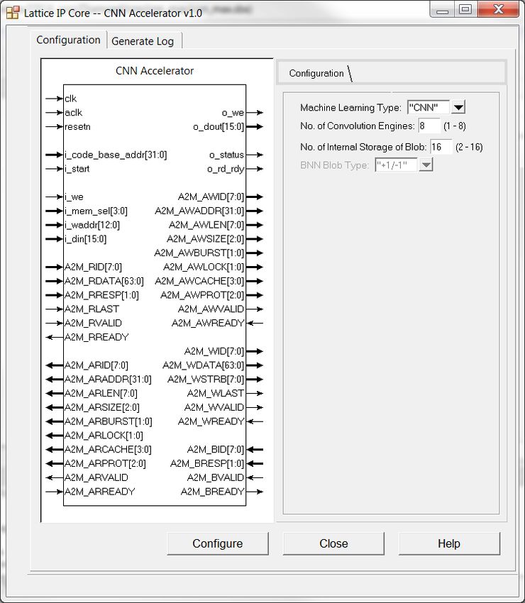
The Clarity Designer tool is used to create IP and architectural modules in the Diamond software. You may refer to the
IP Generation and Evaluation section on how to generate the IP.
Table 3.1 provides the list of user configurable attributes for the CNN Accelerator IP Core. The attribute values are
specified using the IP core Configuration GUI in Clarity Designer as shown in Figure 3.1.
Table 3.1. Attributes Table
Attribute Selectable Values Default Dependency on Other Attributes
Machine Learning Type "CNN", "BNN" "CNN" —
No. of Convolution Engines 1-8 8 —
No. of Internal Storage of Blob 2 - 16 16 —
BNN Blob Type "+1/-1", "+1/0" "+1/-1" Valid only when
Machine Learning Type = "BNN"
Figure 3.1. CNN Accelerator IP Core Configuration GUI
© 2018 Lattice Semiconductor Corp. All Lattice trademarks, registered trademarks, patents, and disclaimers are as listed at www.latticesemi.com/legal. All other brand or product names are
trademarks or registered trademarks of their respective holders. The specifications and information herein are subject to change without notice.
FPGA-IPUG-02037-1.0 13CNN Accelerator IP Core
User Guide
Table 3.2. Attributes Descriptions
Attribute Description
Machine Learning Type This option allows you to choose between CNN engine and BNN engine.
CNN engine always uses 16-bit fixed point weight, while BNN only uses 1-bit weight.
Based on required performance, accuracy and available capacity, you should select
Machine Learning Type.
No. of Convolution Engines This option allows you to specify the number of convolution engines.
For 1D convolution:
1-9 taps can be performed for each engine
Up to 72 taps by chaining 8 engines
For 2D Convolution:
3x3 convolution per cycle per engine
You should trade-off between required size and performance.
No. of Internal Storage of Blob Each storage can store up to 16Kbytes. You should trade-off between required size and
performance. In order to fully utilize convolution engines, number of storage must be
larger than number of convolution engines. Recommend set 2x of number of
convolution engines.
BNN Blob Type Selects the type of binary blob data, either +1/-1 or +1/0. This setting should be
matched to the Lattice Neural Network Compiler.
© 2018 Lattice Semiconductor Corp. All Lattice trademarks, registered trademarks, patents, and disclaimers are as listed at www.latticesemi.com/legal. All other brand or product names are
trademarks or registered trademarks of their respective holders. The specifications and information herein are subject to change without notice.
14 FPGA-IPUG-02037-1.0CNN Accelerator IP Core
User Guide
4. IP Generation and Evaluation
This section provides information on how to generate the IP using the Lattice Diamond software, and how to run
simulation, synthesis and hardware evaluation. For more details on the Lattice Diamond software, you may refer to the
Lattice Diamond User Guide and Lattice Diamond Tutorial.
4.1. Licensing the IP
An IP core-specific device-specific license string is required to enable full, unrestricted use of the Lattice CNN
Accelerator IP Core in a complete, top-level design. You may refer to the instructions on how to obtain licenses for
Lattice IP cores at http://www.latticesemi.com/Products/DesignSoftwareAndIP.aspx.
You may download and generate the CNN Accelerator IP Core and fully evaluate the core through functional simulation
and implementation (synthesis, map, place and route) without an IP license string. The CNN Accelerator IP Core
supports Lattice’s IP hardware evaluation capability, which makes it possible to create versions of the IP core which
operate in hardware for a limited time (approximately four hours) without requiring an IP license string. See Hardware
Evaluation section for further details. However, a license string is required to enable timing simulation to open the
design in the Diamond software, and to generate bitstream file that does not include the hardware evaluation timeout
limitation.
Note: All IP has a license whether in eval mode or full mode. Difference is license string.
4.2. Generation and Synthesis
4.2.1. Getting Started
The CNN Accelerator IP Core is available for download in the Lattice IP Server using the Diamond Clarity Designer tool.
The IP files can be automatically installed using InstallShield® technology in any customer-specified directory. After the
IP core is installed, the IP core is listed in the Catalog tab of the Clarity Designer GUI, under DSP category as shown in
Figure 4.1.
Figure 4.1. CNN Accelerator IP Core in Clarity Designer Catalog Tab
© 2018 Lattice Semiconductor Corp. All Lattice trademarks, registered trademarks, patents, and disclaimers are as listed at www.latticesemi.com/legal. All other brand or product names are
trademarks or registered trademarks of their respective holders. The specifications and information herein are subject to change without notice.
FPGA-IPUG-02037-1.0 15CNN Accelerator IP Core
User Guide
4.2.2. Configuring the IP Core in Clarity
The CNN Accelerator IP Core should be configured and generated before it can be used in the Diamond project. This is
done via CNN Accelerator IP Core configuration GUI (Figure 3.1), it provides an interface for setting the desired
parameters and invoking the IP core generator. This configuration GUI is launch by performing the following:
1. Double-click the CNN Accelerator IP Core in Catalog tab of Diamond Clarity tool.
2. Specify the following in the pop-up window:
Instance Path
Instance Name
Note: All generated files are placed under the directory /.
3. Enter configuration parameters.
4. Click Customize – this step will close the pop-up window and launch the CNN Accelerator IP Core configuration GUI.
Desired parameters are entered in the CNN Accelerator IP Core configuration GUI. Ensure that same parameters are
used in the Lattice Neural Network Compiler to be able to generate compatible command sequence code.
Click the Generate button, and close the GUI to generate the IP core and supporting files.
Table 4.1 provides a list of key files and directories created by the IPexpress tool and how they are used.
Table 4.1. File List
Attribute Description
.lpc This file contains the tool options used to recreate or modify the core in the Clarity tool.
.ngo This file provides the synthesized IP core.
_bb.v This file provides the synthesis black box for the user’s synthesis.
_inst.v This file provides an instance template for the IP core.
_top.v This file provides an example RTL top file that instantiates the IP core.
beh_rtl.v* This file provides cycle-accurate simulation model for the IP core.
The top level module name in this file is .
generate_core.tcl This file is created when the GUI Generate button is pushed.
This file may be run from command line.
_generate.log This is the synthesis and map log file.
_gen.log This is the IP Core generation log file.
*Note: This file is located in the following path:
//ml_engine_ecp5_eval//src/beh_rtl/
4.2.3. Instantiating the IP Core
The generated CNN Accelerator IP Core package includes black-box (_bb.v) and instance (_inst.v) templates that can be used to instantiate the core in a top-level design. A sample of RTL top-level
reference source file (_top.v) that can be used as an instantiation template for the IP core is also
provided. You may also use this top-level reference as the starting template for the top-level for their complete design.
4.3. Running Functional Simulation
The CNN Accelerator IP Core does NOT contain a sample test bench for performing simple simulation test. However, a
cycle-accurate simulation model (beh_rtl.v) is provided as shown in Table 4.1. This may be instantiated in a test bench.
Please note that the following must be performed to be able to successfully elaborate the simulation model:
1. Instantiate GSR and PUR in testbench top RTL file.
The following codes may be copied and paste to testbench top RTL file:
PUR PUR_INST();
GSR GSR_INST();
2. Compile the simulation primitives of selected device. These are located in the following path:
/cae_library/simulation/verilog/
© 2018 Lattice Semiconductor Corp. All Lattice trademarks, registered trademarks, patents, and disclaimers are as listed at www.latticesemi.com/legal. All other brand or product names are
trademarks or registered trademarks of their respective holders. The specifications and information herein are subject to change without notice.
16 FPGA-IPUG-02037-1.0CNN Accelerator IP Core
User Guide
4.4. Hardware Evaluation
The CNN Accelerator IP Core supports Lattice’s IP hardware evaluation capability, which makes it possible to create
versions of the IP core that operate in hardware for a limited period of time (approximately four hours) without
requiring the purchase of an IP license. It may also be used to evaluate the core in hardware in user-defined designs.
Choose Project > Active Strategy > Translate Design Settings. The hardware evaluation capability may be
enabled/disabled in the Strategy dialog box. It is enabled by default.
© 2018 Lattice Semiconductor Corp. All Lattice trademarks, registered trademarks, patents, and disclaimers are as listed at www.latticesemi.com/legal. All other brand or product names are
trademarks or registered trademarks of their respective holders. The specifications and information herein are subject to change without notice.
FPGA-IPUG-02037-1.0 17CNN Accelerator IP Core
User Guide
5. Ordering Part Number
The Ordering Part Numbers (OPN) for CNN Accelerator IP Core targeting ECP5 and ECP5-5G FPGA devices are the
following:
CNN-ACCEL-E5-U – Project License
CNN-ACCEL-E5-UT – Site License
© 2018 Lattice Semiconductor Corp. All Lattice trademarks, registered trademarks, patents, and disclaimers are as listed at www.latticesemi.com/legal. All other brand or product names are
trademarks or registered trademarks of their respective holders. The specifications and information herein are subject to change without notice.
18 FPGA-IPUG-02037-1.0CNN Accelerator IP Core
User Guide
References
For more info on the FPGA device, visit: http://www.latticesemi.com/Products/FPGAandCPLD/ECP5
For complete information on Lattice Diamond Project-Based Environment, Design Flow, Implementation Flow and
Tasks, as well as on the Simulation Flow, see the Lattice Diamond User Guide.
Technical Support Assistance
Submit a technical support case through www.latticesemi.com/techsupport.
© 2018 Lattice Semiconductor Corp. All Lattice trademarks, registered trademarks, patents, and disclaimers are as listed at www.latticesemi.com/legal. All other brand or product names are
trademarks or registered trademarks of their respective holders. The specifications and information herein are subject to change without notice.
FPGA-IPUG-02037-1.0 19CNN Accelerator IP Core
User Guide
Appendix A. Resource Utilization
Table A-1. Performance and Resource Utilizationshows configuration and resource utilization for the ECP5UM using
Lattice Diamond 3.10.0.111.0. The following settings are used in generating this data:
Synthesis Tool: Synplify Pro
Device Part No.: LFE5UM-85F-8BG756I
BNN Blob Type: +1/0 (For Machine Learning Type: BNN)
Table A-1. Performance and Resource Utilization*1
No. of Convolution No. of Internal Register LUTs Slices Block RAMs clk Fmax3
Engines Storage of Blob*2 (MHz)
Machine Learning Type: CNN
1 2 3332 4353 3246 25 120.525
4 8 8745 13137 9665 76 115.101
8 16 15914 24891 18065 144 107.654
Machine Learning Type: BNN
1 2 3304 4592 3301 25 116.782
4 8 9379 14442 10206 76 112.740
8 16 17411 27555 19187 144 110.509
Notes:
1. Performance may vary when using a different software version or targeting a different device density or speed grade.
2. It is recommended to use No. of Internal Storage of Blob = 2 * No. of Convolution Engines.
3. Fmax is generated when the FPGA design only contains CNN Accelerator IP Core, these values may be reduced when
user logic is added to the FPGA design.
For more information on Lattice Diamond Software, visit the Lattice web site at
www.latticesemi.com/Products/DesignSoftwareAndIP.
© 2018 Lattice Semiconductor Corp. All Lattice trademarks, registered trademarks, patents, and disclaimers are as listed at www.latticesemi.com/legal. All other brand or product names are
trademarks or registered trademarks of their respective holders. The specifications and information herein are subject to change without notice.
20 FPGA-IPUG-02037-1.0CNN Accelerator IP Core
User Guide
Revision History
Date Version Change Summary
May 2018 1.0 Initial release.
© 2018 Lattice Semiconductor Corp. All Lattice trademarks, registered trademarks, patents, and disclaimers are as listed at www.latticesemi.com/legal. All other brand or product names are
trademarks or registered trademarks of their respective holders. The specifications and information herein are subject to change without notice.
FPGA-IPUG-02037-1.0 217th Floor, 111 SW 5th Avenue
Portland, OR 97204, USA
T 503.268.8000
www.latticesemi.comYou can also read