APPLICATION NOTE UNIVERSAL CLASS D (UCD) POWER AMPLIFIER USING HV PAK
←
→
Page content transcription
If your browser does not render page correctly, please read the page content below
Application Note
    Universal Class D (UcD) Power
       Amplifier Using HV PAK
                                      AN-CM-322

Abstract
This application note describes how to design and build a stereo full-bridge Universal Class D (UcD)
audio power amplifier using the SLG47105 IC.
The application note comes complete with a design file that can be found in the Reference section.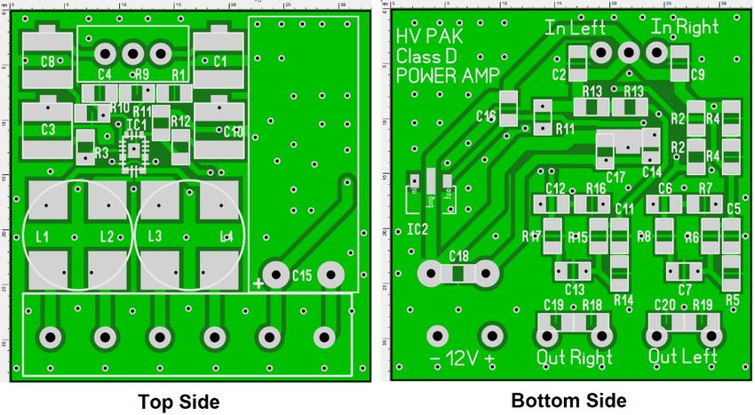
AN-CM-322
Universal Class D (UcD) Power Amplifier Using HV PAK

Contents
Abstract .............................................................................................................................1
Contents ............................................................................................................................2
Figures ..............................................................................................................................2
Tables................................................................................................................................2
1    Terms and Definitions....................................................................................................3
2    Introduction ..................................................................................................................4
     2.1 Basic Class D Topology ..........................................................................................4
     2.2 Phase-shift Control Using the Reconstruction Filter Topology .......................................5
3    Design Operation. .........................................................................................................6
     3.1 Schematic Design ..................................................................................................6
     3.2 Typical Operating Characteristics .............................................................................8
     3.3 Macrocell Configuration...........................................................................................9
     3.4 PCB Layout Consideration..................................................................................... 10
4    Conclusions................................................................................................................ 11
Revision History............................................................................................................... 12

Figures
Figure 1: Half-Bridge Class D Amplif ier, Basic Topology .............................................................4
Figure 2: The Output-Signal Pulse Widths Vary Proportionally With the Input-Signal.......................5
Figure 3: Phase-Shift Control Using the Reconstruction Filter Topology ........................................5
Figure 4: Phase-Shift ............................................................................................................6
Figure 5: Stereo Full-bridge UcD Audio Power Amplifier Project ..................................................7
Figure 6: Simplified Circuit of the Amplif ier. One Channel ...........................................................7
Figure 7: THD vs Output Power, Rl = 8 Ohm, Gain = 22.5 dB, f = 1kHz ........................................8
Figure 8: THD vs Frequency, Rl = 8 Ohm, Gain = 22.5 dB, Pout = 1 W .........................................9
Figure 9: Frequency response, VDD = 12V, Rl = 8 ,Gain = 22.5 dB..............................................9
Figure 10: Test PCB Design................................................................................................. 11
Figure 11: Test PCB Photo .................................................................................................. 11

Tables
Table 1: PIN settings.............................................................................................................9
Table 2: ACMP Settings ...................................................................................................... 10
Table 3: HV Output Settings................................................................................................. 10

Application Note                                        Revision 1.0                                                15-Sept-2021

CFR0014                                                       2 of 13                                    © 2021 Dialog Semiconductor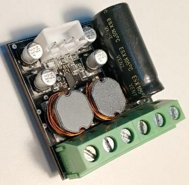
AN-CM-322
Universal Class D (UcD) Power Amplifier Using HV PAK

1     Terms and Definitions
ACMP               Analog Comparator
GPO                General Purpose Output
HV                 High Voltage
IC                 Integrated Circuit
I/O                Input / Output
LDO                Low Drop-out
MOSFET             Metal–oxide–semiconductor Field-effect TransistorReferences
PWM                Pulse Width Modulation
THD + N            Total Harmonic Distortion Plus Noise
UcD                Universal Class D

For related documents and software, please visit:
https://www.dialog-semiconductor.com/configurable-mixed-signal

Download our free GreenPAK Designer software [1] to open the .gp file [2] and use the GreenPAK
development tools [3] to freeze the design into your own customized IC in a matter of minutes.
Dialog Semiconductor provides a complete library of application notes [4] featuring design examples
as well as explanations of features and blocks within the Dialog IC.

[1] GreenPAK Designer Software, Software Download, and User Guide, Dialog Semiconductor
[2] AN-CM-322 Universal Class D (UcD) Power Amplifier Using HV PAK.gp, GreePAK Design File,
     Dialog Semiconductor
[3] GreenPAK Development Tools, GreenPAK Development Tools Webpage, Dialog Semiconductor
[4] GreenPAK Application Notes, GreenPAK Application Notes Webpage, Dialog Semiconductor
[5] SLG47105 Datasheet, Dialog Semiconductor
[6] AN-CM-321 Class D Power Amplifier Using HV PAK
[7] Simple Self-Oscillating Class D Amplifier with Full Output Filter Control by Bruno Putzeys, May
     2010
[8] A Universal Grammar of Class D Amplification by Bruno Putzeys, Hypex Electronics, The
     Netherlands, May 2007
[9] UM10155, Discrete Class D High Power Audio Amplifier, Rev. 02 — 5 September 2006
[10]    WO 2003/090343 A3, Rev. 02 — 5 September. International application published under the
   patent cooperation treaty (PCT)

Author: Nazar Sliunchenko

Application Note                          Revision 1.0                                 15-Sept-2021

CFR0014                                       3 of 13                        © 2021 Dialog Semiconductor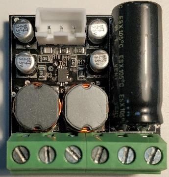
AN-CM-322
Universal Class D (UcD) Power Amplifier Using HV PAK

2         Introduction
This application note describes how to design and build a stereo f ull-bridge Universal Class D (UcD)
audio power amplifier using the SLG47105 IC.
A class D amplif ier operates by deriving a two -state signal f rom a continuous control signal and
amplifying it using power switches. At the core of every class D amplifier is at least one comparator
and one switching power stage. In all but the low-cost power amplifiers, a passive LC f ilter is added.
Here’s a summary of the benef its and disadvantages of the Class -D amplifier versus the traditional
Class-AB amplifier.
     •     Class AB
Benef it: Lowest distortion—total harmonic distortion plus noise (THD + N) is less than 0.1% f or high
f idelity.
Disadvantages: Inefficient—maximum possible efficiency is about 60%. High power consumption and
significant heat generation. It’s also larger in size.
     •     Class D
Benef its: High efficiency—greater than 90%. Less power consumption and lower heat generation.
Smaller size. Very high-power potential (400 to 500 W) in a small package.
Disadvantages: High-frequency noise generation.

    2.1     Basic Class D Topology
The most basic topology utilizes pulse-width modulation (PWM) with a triangle-wave (or sawtooth)
oscillator. Figure 1 shows a simplified block diagram of a PWM-based, half-bridge Class D amplifier. It
consists of a pulse-width modulator, two output MOSFETs, and an external lowpass f ilter (L F and CF)
to recover the amplified audio signal. As shown in the f igure, both MOSFETs operate as current-
steering switches by alternately connecting the output node to V DD and ground, thus the resulting output
of a Class D amplifier is a high-f requency square wave. The output square wave is pulse-width
modulated by the input audio signal. PWM is accomplished by comparing the input audio signal to an
internally generated triangle-wave (or sawtooth) oscillator. The resulting duty cycle of the square wave
is proportional to the level of the input signal. When no input signal is present, the duty cycle of the
output waveform is equal to 50%. Figure 2 illustrates the resulting PWM output waveform due to the
varying input-signal level.
This basic topology has a few downsides. Very low power supply rejection ratio. High THD. The quality
of the output signal is highly dependent on the linearity and stability of the tri angle wave, which
significantly complicates the circuit.

                      Figure 1: Half-Bridge Class D Amplifier, Basic Topology

Application Note                            Revision 1.0                                   15-Sept-2021

CFR0014                                         4 of 13                          © 2021 Dialog Semiconductor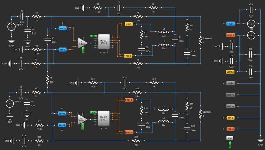
AN-CM-322
Universal Class D (UcD) Power Amplifier Using HV PAK

     Figure 2: The Output-Signal Pulse Widths Vary Proportionally With the Input-Signal

One of the most commonly used topologies of class D audio amplifiers is known as self -oscillation.
Self -oscillating class D audio amplifiers are characterized by having an open-loop bandwidth equal to
the switching frequency as opposed to traditional PWM amplifiers, where the loop bandwidth typically
will be limited to one-tenth of the switching frequency. This increased loop bandwidth provides valuable
loop gain at low frequency, which is beneficial with respect to the reduction of Total Harmonic Distortion
(THD).
There are several ways of designing a self -oscillating class D power amp, but in this document, only
Phase-shift control using the reconstruction filter topology (UcD) will be considered, as this
topology provides the best audio performance and ensures the highest sound quality.

  2.2     Phase-shift Control Using the Reconstruction Filter Topology
The phase shift of the reconstruction filter is usually seen as a burden, rarely as an advantage.
Second-order filters turn out to be very interesting for building phaseshift controlled amplifiers. One is
reminded that the switching frequency is set well beyond the corner frequency of the filter. At any
suf ficiently high frequency, a second-order low pass filter produces a phase shift close to 180
degrees. Varying load conditions only affect this to the order of a few degrees.
Closing a negative feedback loop around such a f ilter is not enough though. The oscillation occurs at
a phase shift of exactly 180 degrees (the other 180 degrees are f urnished by the polarity inversion),
which only happens at infinity. An additional network is in order that holds the phase shift well away
f rom 180 degrees below the desired switching frequency, and another one that pushes it well beyond
it above this frequency. Any practical circuit will already have the latter for free. The combined
propagation delays of the comparator and the power stage constitute a phase shift directly
proportional to frequency. The f ormer can be as simple as a phase lead network in the feedback
path. See Figure 3.

                 Figure 3: Phase-Shift Control Using the Reconstruction Filter Topology

Application Note                            Revision 1.0                                    15-Sept-2021

CFR0014                                          5 of 13                          © 2021 Dialog Semiconductor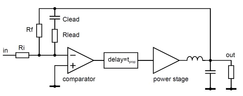
AN-CM-322
Universal Class D (UcD) Power Amplifier Using HV PAK

Since at any useful oscillation frequency the phase shift of the output filter is 180 degrees, oscillation
will occur at the frequency where the propagation delay and the phase lead cancel out. Care should
be taken to ensure that under any realistic load condition there is not a second point with 180
degrees phase shift, because this point will be most certainly be the physical resonance frequency
f ilter. Failing this usually leads to the undoing of the amplifier the first time it is overdriven with no
load attached. See Figure 4.

             Where Hlpf is the transfer function of the LC filter and Hfbn that of the feedback network
                 Delay(s) is a linear phase shift function representing the propagation delay.
                                             Figure 4: Phase-Shift

The phase-shift control using the reconstruction filter topology has a big advantage over other
topologies. The negative feedback loop is encompassing the reconstruction filter, this allows to
completely compensate for any non-linearity. The amplifier designed using this topology is capable of
producing extremely low THD+N and can compete with class AB while having all advantages of
class D.

3         Design Operation.
    3.1     Schematic Design
Designing a class D power amp using the SLG47105 IC has its advantages. The chip has two full -
bridge high-speed power outputs which allow building a stereo full-bridge UcD audio power amplifier
using a minimum of internal and external components. See Figure 5 for a complete schematic
diagram in the GreenPAK Designer project. The amplifier operates exactly as described in
Section 2.2. The only difference is a f ull-bridge output. Also, the output (reconstruction) filter is
designed to use a single ferrite core for both L1 and L2 (L3 and L4). It should be noted that the
windings of the coils should be connected in accordance with the sc hematics. The beginning of each
winding is marked with a dot near the coil symbol, see Figure 5.

Application Note                             Revision 1.0                                    15-Sept-2021

CFR0014                                          6 of 13                           © 2021 Dialog Semiconductor
AN-CM-322
Universal Class D (UcD) Power Amplifier Using HV PAK
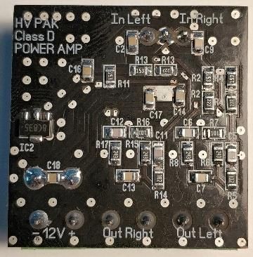
Figure 5: Stereo Full-bridge UcD Audio Power Amplifier Project
It is also possible to use a separate LC f ilter for each output, four in total in this design. But this will
only increase the quantity of the external components leading to a larger PCB size and higher overall
cost.
Since this design is a stereo amp, it means both channels will oscillate with very close frequencies.
That may cause an extra high-frequency interference. To overcome this issue both channels must be
synchronized, it is done by C4 and R9. These components must be selected so the phase shift
between oscillations is as minimal as possible, down to nanoseconds.
The oscillating frequency doesn’t depend much on factors such as parasitic RCL parameters of the
PCB and the IC itself. The main components that set up the frequency are the output filter and R5 C5
chain (R15 C11 f or another channel). Using the values shown on the schematic diagram the
f requency is close to 300kHz.
The amp is powered by a 12 V power supply for VDD2A and VDD2B, also a 5 V LDO IC is used to
power VDD. Since the ACMPs inside the HV PAK are powered from 5 V and the output s tages are
powered from 12 V, the additional voltage divider is required to prevent damaging ACMPs via the
f eedback loop. Figure 6 shows a simplified circuit where the additional voltage dividing resistors are
marked red. Also marked R2, R4, R11, and R13 in Figure 5.
Figure 6: Simplified Circuit of the Amplifier. One Channel
Application Note Revision 1.0 15-Sept-2021
CFR0014 7 of 13 © 2021 Dialog SemiconductorAN-CM-322
Universal Class D (UcD) Power Amplifier Using HV PAK
3.2 Typical Operating Characteristics
Note that connecting speakers of less than 8 Ohm is not recommended unless an additional heat
dissipation is considered.
The amplifier has the following characteristics:
• Power supply voltage – 7.5 V to 12 V
• Current consumption (no input signal) – 40 mA
• Output power per channel (supply – 12V, load – 8 Ohm) – 9 W (max)
• Gain – 22.5 dB
• Input resistance – 2 kOhm
• THD (1 W, 1 kHz) – 0.02%
• THD (9 W, 1 kHz) – 1%
• Frequency response – 20 Hz to 20 kHz (-3 dB)
T HD V S O U T P U T P O WER
1.20%
1.00%
0.80%
0.60%
0.40%
0.20%
0.00%
0.1 0.3 0.5 1.0 2.0 4.0 6.0 8.0 9.0
Figure 7: THD vs Output Power, Rl = 8 Ohm, Gain = 22.5 dB, f = 1kHz
Application Note Revision 1.0 15-Sept-2021
CFR0014 8 of 13 © 2021 Dialog SemiconductorAN-CM-322
Universal Class D (UcD) Power Amplifier Using HV PAK
TH D V S F REQUENCY
0.35%
0.30%
0.25%
0.20%
0.15%
0.10%
0.05%
0.00%
15,000
10,000
20,000
50
20
2,000
8,000
1,000
4,000
200
500
100
300
750
Figure 8: THD vs Frequency, Rl = 8 Ohm, Gain = 22.5 dB, Pout = 1 W
Figure 9: Frequency Response, VDD = 12V, Rl = 8 ,Gain = 22.5 dB
3.3 Macrocell Configuration
Table 1: PIN settings
Properties PIN 7, 8, 9, and 10 PIN 3, 17, 19, and 20
I/O selection Digital output Analog input/output
Input mode OE=0 None Analog input/output
Application Note Revision 1.0 15-Sept-2021
CFR0014 9 of 13 © 2021 Dialog SemiconductorAN-CM-322
Universal Class D (UcD) Power Amplifier Using HV PAK
Output mode OE=1 HIGH and LOW side Analog input/output
Resistor -- Floating
Resistor value -- Floating
Table 2: ACMP Settings
Properties ACMP0H ACMP1H
Hysteresis Disable Disable
IN+ gain Disable Disable
Connections
IN+ source PIN 19 (GPIO5) PIN 20 (GPIO6)
IN- source Ext. Vref (PIN 3 (GPI)) Ext. Vref (PIN 17 (GPIO4))
Table 3: HV Output Settings
Properties HV OUT CTRL0 HV OUT CTRL1
Slew rate Fast for pre-driver mode Fast for pre-driver mode
HV OUT mode Full bridge Half-bridge
Mode control PH-EN IN-IN
Thermal shutdown Enable None
OCP deglitch time enable Without deglitch time Without deglitch time
Control delay of OCP0 retry Delay 492 us Delay 492 us
Control delay of OCP1 retry Delay 492 us Delay 492 us
VDD2A UVLO Desable Desable
3.4 PCB Layout Consideration
PCB should have enough ground plane to dissipate heat. SLG47105 has two additional pads which
provide enhanced thermal dissipation. Thermal vias are used to transfer heat from the chip to other
layers of the PCB. When using loading less than 8 Ohm please attach an ad ditional radiator to
dissipate heat generated by the chip.
The power capacitors should be placed as close as possible to the chip for reducing parasitic
parameters. Also, both the input signal ground and the power ground should be separated and
connected together on the large capacitor, C15 in this project. See test PCB designed for this
application in Figure 10 and Figure 11. The size of the board is 33 x 34 mm.
Application Note Revision 1.0 15-Sept-2021
CFR0014 10 of 13 © 2021 Dialog SemiconductorAN-CM-322
Universal Class D (UcD) Power Amplifier Using HV PAK
Figure 10: Test PCB Design
Figure 11: Test PCB Photo
4 Conclusions
As can be seen, designing and building a stereo full-bridge Universal Class D (UcD) audio power
amplifier using the HV PAK is very easy. The design shown in this document is the simplest version
of the device that can be built based on the SLG47105. There are plenty of unused macrocells that
can be used to design additional functions such as Mute, Enable, Stand By, Overcurrent , and
Overtemperature protection with indication, etc.
Application Note Revision 1.0 15-Sept-2021
CFR0014 11 of 13 © 2021 Dialog SemiconductorAN-CM-322 Universal Class D (UcD) Power Amplifier Using HV PAK Revision History Revision Date Description 1.0 15-Sept-2021 Initial Version Application Note Revision 1.0 15-Sept-2021 CFR0014 12 of 13 © 2021 Dialog Semiconductor
AN-CM-322
Universal Class D (UcD) Power Amplifier Using HV PAK

Status Definitions
 Status                 Definition

                        The content of this document is under review and subject to formal approval, which may result in modifications or
 DRAFT
                        additions.
 APPROVED
                        The content of this document has been approved for publication.
 or unmarked

Disclaimer
Unless otherwise agreed in writing, the Dialog Semiconductor products (and any associated software) referred to in this document are not
designed, authorized, or warranted to be suitable for use in life support, life-critical or safety-critical systems or equipment, nor in applications
where failure or malfunction of a Dialog Semiconductor product (or associated software) can reasonably be expected to result in personal injury,
death or severe property or environmental damage. Dialog Semiconductor and its suppliers accept no liability f or the inclusion and/or use of
Dialog Semiconductor products (and any associated software) in such equipment or applications and therefore such inclusion and/or use is at
the customer’s own risk.
Information in this document is believed to be accurate and reliable. However, Dialog Semiconductor does not give any representations or
warranties, express or implied, as to the accuracy or completeness of such information. Dialog Semiconductor furthermore takes no
responsibility whatsoever for the content in this document if provided by any information source outside of Dialog Semiconductor.
Dialog Semiconductor reserves the right to change without notice the information published in this document, including, without limitation, the
specification and the design of the related semiconductor products, software, and applications. Notwithstanding the foregoing, for any
automotive-grade version of the device, Dialog Semiconductor reserves the right to change the information published in this document,
including, without limitation, the specification and the design of the related semiconductor products, software, and applications, in accordance
with its standard automotive change notification process.
Applications, software, and semiconductor products described in this document are for illustrative purposes only. Dialog Semiconductor makes
no representation or warranty that such applications, software, and semiconductor products will be suitable for the specified use without further
testing or modification. Unless otherwise agreed in writing, such testing or modification is the sole responsibility of the customer and Dialog
Semiconductor excludes all liability in this respect.
Nothing in this document may be construed as a license for the customer to use the Dialog Semiconductor products, software, and applications
referred to in this document. Such license must be separately sought by the customer with Dialog Semiconductor.
All use of Dialog Semiconductor products, software, and applications referred to in this document is subject to Dialog Semiconductor’s Standard
Terms and Conditions of Sale, available on the company website (www.dialog-semiconductor.com) unless otherwise stated.
Dialog, Dialog Semiconductor, and the Dialog logo are trademarks of Dialog Semiconductor Plc or its subsidiaries. All other product or service
names and marks are the property of their respective owners.

© 2021 Dialog Semiconductor. All rights reserved.

Contacting Dialog Semiconductor
United Kingdom (Headquarters)        North America                        Hong Kong                                China (Shenzhen)
Dialog Semiconductor (UK) LTD        Dialog Semiconductor Inc.            Dialog Semiconductor Hong Kong           Dialog Semiconductor China
Phone: +44 1793 757700               Phone: +1 408 845 8500               Phone: +852 2607 4271                    Phone: +86 755 2981 3669
Germany                              Japan                                Korea                                    China (Shanghai)
Dialog Semiconductor GmbH            Dialog Semiconductor K. K.           Dialog Semiconductor Korea               Dialog Semiconductor China
Phone: +49 7021 805-0                Phone: +81 3 5769 5100               Phone: +82 2 3469 8200                   Phone: +86 21 5424 9058
The Netherlands                      Taiwan
Dialog Semiconductor B.V.            Dialog Semiconductor Taiwan
Phone: +31 73 640 8822               Phone: +886 281 786 222
Email:                               Web site:
enquiry@diasemi.com                  www.dialog-semiconductor.com

Application Note                                              Revision 1.0                                                      15-Sept-2021

CFR0014                                                             13 of 13                                        © 2021 Dialog Semiconductor
You can also read