7 SERIES FPGAS AND ZYNQ-7000 SOC XADC DUAL 12-BIT 1 MSPS ANALOG-TO-DIGITAL CONVERTER - USER GUIDE - XILINX
←
→
Page content transcription
If your browser does not render page correctly, please read the page content below
7 Series FPGAs and
Zynq-7000 SoC XADC Dual
12-Bit 1 MSPS
Analog-to-Digital Converter
User Guide

UG480 (v1.10.1) July 23, 2018
Notice of Disclaimer
The information disclosed to you hereunder (the “Materials”) is provided solely for the selection and use of Xilinx products. To the maximum
extent permitted by applicable law: (1) Materials are made available “AS IS” and with all faults, Xilinx hereby DISCLAIMS ALL
WARRANTIES AND CONDITIONS, EXPRESS, IMPLIED, OR STATUTORY, INCLUDING BUT NOT LIMITED TO WARRANTIES OF
MERCHANTABILITY, NON-INFRINGEMENT, OR FITNESS FOR ANY PARTICULAR PURPOSE; and (2) Xilinx shall not be liable (whether
in contract or tort, including negligence, or under any other theory of liability) for any loss or damage of any kind or nature related to, arising
under, or in connection with, the Materials (including your use of the Materials), including for any direct, indirect, special, incidental, or
consequential loss or damage (including loss of data, profits, goodwill, or any type of loss or damage suffered as a result of any action
brought by a third party) even if such damage or loss was reasonably foreseeable or Xilinx had been advised of the possibility of the same.
Xilinx assumes no obligation to correct any errors contained in the Materials or to notify you of updates to the Materials or to product
specifications. You may not reproduce, modify, distribute, or publicly display the Materials without prior written consent. Certain products are
subject to the terms and conditions of Xilinx’s limited warranty, please refer to Xilinx’s Terms of Sale which can be viewed at
www.xilinx.com/legal.htm#tos; IP cores may be subject to warranty and support terms contained in a license issued to you by Xilinx. Xilinx
products are not designed or intended to be fail-safe or for use in any application requiring fail-safe performance; you assume sole risk and
liability for use of Xilinx products in such critical applications, please refer to Xilinx’s Terms of Sale which can be viewed at
www.xilinx.com/legal.htm#tos.
AUTOMOTIVE APPLICATIONS DISCLAIMER
AUTOMOTIVE PRODUCTS (IDENTIFIED AS “XA” IN THE PART NUMBER) ARE NOT WARRANTED FOR USE IN THE DEPLOYMENT
OF AIRBAGS OR FOR USE IN APPLICATIONS THAT AFFECT CONTROL OF A VEHICLE (“SAFETY APPLICATION”) UNLESS THERE
IS A SAFETY CONCEPT OR REDUNDANCY FEATURE CONSISTENT WITH THE ISO 26262 AUTOMOTIVE SAFETY STANDARD
(“SAFETY DESIGN”). CUSTOMER SHALL, PRIOR TO USING OR DISTRIBUTING ANY SYSTEMS THAT INCORPORATE PRODUCTS,
THOROUGHLY TEST SUCH SYSTEMS FOR SAFETY PURPOSES. USE OF PRODUCTS IN A SAFETY APPLICATION WITHOUT A
SAFETY DESIGN IS FULLY AT THE RISK OF CUSTOMER, SUBJECT ONLY TO APPLICABLE LAWS AND REGULATIONS GOVERNING
LIMITATIONS ON PRODUCT LIABILITY.
© Copyright 2011–2018 Xilinx, Inc. Xilinx, the Xilinx logo, Artix, ISE, Kintex, Spartan, Virtex, Vivado, Zynq, and other designated brands
included herein are trademarks of Xilinx in the United States and other countries. All other trademarks are the property of their respective
owners.

XADC User Guide                                                 www.xilinx.com                                 UG480 (v1.10.1) July 23, 2018
Revision History
The following table shows the revision history for this document.

     Date          Version                                                 Revision
 03/01/2011          1.0        Initial Xilinx release.
 03/28/2011          1.1        Added “Dual 12-Bit MSPS Analog-to-Digital Converter” to document title. Modified
                                first paragraph and added second paragraph in Chapter 1, Introduction and Quick Start.
                                Added Table 1-1. Removed the Thermal Diode (DXP and DXN) section from Chapter 4.
 10/25/2012          1.2        This version was updated to include information for the Zynq-7000 SoC devices: Added
                                “Zynq-7000 SoC” to document title.
                                In Figure 1-1 Zynq-7000 SoC information was added and the control and status registers
                                changed from 32 x 16 bits to 64 x 16 bits. The System Monitor Support section changed to
                                Differences between Virtex-5 and Virtex-6 System Monitors. Functionality for the XADC
                                block in 7 series FPGAs is now defined for previously undefined status registers in
                                subsequent chapters. Capacitor values in Figure 1-2 changed, and a note was added
                                about the placement of 100 nF decoupling capacitors. In Table 1-1, for VREFP_0, GND
                                changed to GNDADC, accurate reference source changed to accurate reference IC, and
                                VP_0 and VN_0 types were changed to dedicated analog inputs. Footnotes were added to
                                support 7 series and Zynq device pin packages. A note about application guidelines was
                                added after Table 1-1. Information about auxiliary analog channels was added to the
                                External Analog Inputs section. In Table 1-2, ports ALM[0] through [ALM[3] have XADC
                                removed from the description. Alarms specific to Zynq-7000 SoC devices (ALM[4],
                                ALM[5], and ALM[6]) were added. The example in Example Instantiation was updated.
                                In ADC and Sensors, information about an analog input signal of 200 mV was modified,
                                and Equation 1-1 was added. A new Zynq-7000 SoC subsection was added to the end of
                                the chapter.
                                In ADC Transfer Functions MSBs are defined as left-most bits. In Auxiliary Analog
                                Inputs in the instantiation was changed to on the primitive, and information that
                                configuration is automatic when analog inputs are connected was added. The Note on
                                page 29 was expanded to clarify device support of auxiliary analog channels.
                                Equation 2-2 was added (unipolar mode), Equation 2-1, Equation 2-3, and Equation 2-4
                                were modified (“10”was changed to “9”), and the paragraph following Equation 2-4 was
                                added. Information about additional external resistance was added to Unipolar Input
                                Signals. In Temperature Sensor this sentence was deleted: “The on-chip temperature
                                sensor has a maximum measurement error of ±4°C over a range of –40°C to +125°C.”
                                Information was added to the Power Supply Sensor section about which supplies are
                                monitored and where measurements are stored for Zynq-7000 SoC devices.

UG480 (v1.10.1) July 23, 2018                             www.xilinx.com                               XADC User Guide
Date          Version                                           Revision
 10/25/2012         1.2      Min/max register lists were updated for Zynq-7000 SoC devices in Figure 3-1. In
                  (Cont’d)   Table 3-1 the VREFN description was updated, new Zynq-7000 device channels VCCPINT,
                             VCCPAUX, and VCCO_DDR were added. Zynq-7000 SoC status registers were added to
                             Figure 3-1. Flag registers for DI5 through DI8 in Figure 3-2 changed and DIS was
                             removed from Table 3-2. XADC Calibration Coefficients were added. Configuration
                             registers ALM[4], ALM[5], and ALM[6] were added to Figure 3-4. In Table 3-3, a new
                             row was added for bits DI19 to DI11. In Table 3-7, rows for ADC channels 13, 14, and 15
                             were added. Zynq-7000 SoC alarm threshold register information was added to Alarm
                             Registers (50h to 5Fh). A note in the section DRP JTAG Interface mentions conditions in
                             which the external JTAG access is disabled for Zynq devices. Section Zynq-7000 SoC
                             Processing System (PS) to XADC Dedicated Interface was added to the end of the
                             chapter.
                             In XADC Operating Modes, operate both ADCs in parallel in the first paragraph changed
                             to operate both ADCs in lock step. In Single Channel Mode, the first sentence was deleted
                             (“Single channel mode is the most basic way users can modify the operation of the
                             XADC.”) Sequence numbers and descriptions in Table 4-1 and Table 4-2 changed and
                             were added for Zynq-7000 SoC devices. In Sequencer Modes, default mode sequences
                             were changed in Table 4-3 and added for Zynq-7000 SoC devices. The sentence before
                             Table 4-4 was deleted. The footnote in Table 4-4 and Table 4-6 was enhanced to mention
                             auxiliary analog channel support. Table 4-7 was updated to include Zynq-7000 SoC
                             channels. Alarm threshold registers for the Zynq-7000 SoC were added to Table 4-8. A
                             new section XADC Enhanced Linearity Mode and Figure 4-5 were added to the end of
                             the chapter.
                             The Dynamic Reconfiguration Port (DRP) Timing section was added. Removed
                             Table 5-1: XADC Timing Information.
                             In Reference Inputs (VREFP and VREFN), added “Noise on the reference voltage also adds
                             noise to the ADC conversion and results in more code transition noise or poorer than
                             expected SNR” to the end of the first paragraph. Capacitor values were changed, a new
                             10 µF capacitor was added, and notes were added to Figure 6-1. Notes were added to
                             Figure 6-5. XADC Software Support was completely replaced. In that section, the Verilog
                             instantiation was replaced. Figure 6-6: Analog Stimulus File and Figure 6-7: XADC
                             Simulation Output were deleted. In the new section, Figure 6-5 through Figure 6-8 were
                             added.
 03/10/2014         1.3      Updated the disclaimer and copyright. Changes to Figure 1-2 in XADC Pinout
                             Requirements. In External Analog Inputs, clarified how auxiliary analog inputs are
                             handled in Vivado tools. Improved description of RESET signal in Table 1-2. In
                             Adjusting the Acquisition Settling Time, added to description of ACQ bit. In Analog
                             Input Description, added note to Equation 2-1. Added Table 3-3, Calibration Coefficients
                             in Status Register. Added to description of DI4 and DI5 in Table 3-5. Added to important
                             note in DRP JTAG Interface. Added clarification to Table 4-1 and Table 4-2 in ADC
                             Channel Selection Registers (48h and 49h) section. Modified Figure 4-3. Added note to
                             Table 4-8, Alarm Threshold Registers. Changes to description of Thermal Management.
                             Modified Figure 5-1. Updated Conversion Phase and Event-Driven Sampling. Added to
                             description of Acquisition Phase. Updated External Analog Inputs. Modified Figure 6-3.
                             Modified Example Design Instantiation and Example Design Test Bench. Updated Using
                             XADC Instantiation Wizard. Updated Figure 6-7.
  04/9/2014        1.3.1     Updated link to UG585 in References.
 05/31/2014         1.4      Updated Figure 1-2, Figure 2-10, and Figure 3-3. Updated VREFP_0 package pin
                             description in Table 1-1. Updated Gain Coefficients and Single Pass Mode. Added
                             second paragraph to Chapter 4, XADC Operating Modes introduction.

XADC User Guide                                   www.xilinx.com                         UG480 (v1.10.1) July 23, 2018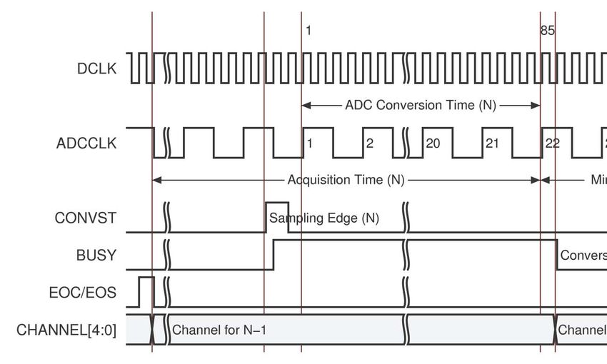
Date          Version                                            Revision
 10/21/2014          1.5        Clarified 7 series terminology throughout. Updated Preface to include Zynq-7000 SoC
                                description, and added link to design files. Modified location of ferrite beads in
                                Figure 1-2 and Figure 6-1. Added equation and explanation to XADC DRP JTAG Write
                                Operation in Chapter 3. Modified Thermal Management in Chapter 4, including adding
                                three equations and Figure 4-4. Added Vivado design tools information to XADC
                                Enhanced Linearity Mode. Added settling period information to Event-Driven
                                Sampling. Updated Figure 5-2 and removed timing information from Figure 5-3.
                                Updated Figure 6-7.
 01/30/2015          1.6        Updated Over and Under Voltages.
 02/04/2015         1.6.1       Made typographical edits.
 05/19/2015          1.7        Updated Reference Inputs (VREFP and VREFN) and External Analog Inputs.
 05/24/2016          1.8        Updated External Analog Inputs and Auxiliary Analog Inputs. Changed INIT_53 in
                                examples to 125°C with automatic shutdown. Updated VCCO_DDR address in Table 4-3.
                                Updated Equation 4-1 and Equation 4-3. Standardized figure format.
 09/27/2016          1.9        Added Spartan-7 devices throughout.
                                Updated introductory paragraph in About This Guide. Added DS180 to References.
 12/23/2017          1.10       Added a second note to Table 3-12. Standardized figure format.
 07/23/2018         1.10.1      Typographical updates.

UG480 (v1.10.1) July 23, 2018                       www.xilinx.com                                 XADC User Guide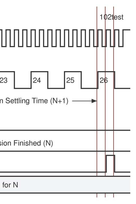
XADC User Guide www.xilinx.com UG480 (v1.10.1) July 23, 2018
Table of Contents

                Revision History . . . . . . . . . . . . . . . . . . . . . . . . . . . . . . . . . . . . . . . . . . . . . . . . . . . . . . . . . . . . . 3

        Preface: About This Guide
                Guide Contents . . . . . . . . . . . . . . . . . . . . . . . . . . . . . . . . . . . . . . . . . . . . . . . . . . . . . . . . . . . . . 11
                Additional Resources . . . . . . . . . . . . . . . . . . . . . . . . . . . . . . . . . . . . . . . . . . . . . . . . . . . . . . . 11
                References . . . . . . . . . . . . . . . . . . . . . . . . . . . . . . . . . . . . . . . . . . . . . . . . . . . . . . . . . . . . . . . . . . 12

        Chapter 1: Introduction and Quick Start
                XADC Overview . . . . . . . . . . . . . . . . . . . . . . . . . . . . . . . . . . . . . . . . . . . . . . . . . . . . . . . . . . . . 13
                       Differences between Virtex-5 and Virtex-6 System Monitors . . . . . . . . . . . . . . . . . . . . 14
                XADC Pinout Requirements. . . . . . . . . . . . . . . . . . . . . . . . . . . . . . . . . . . . . . . . . . . . . . . . . 15
                       Dedicated Package Pins . . . . . . . . . . . . . . . . . . . . . . . . . . . . . . . . . . . . . . . . . . . . . . . . . . . 15
                       External Analog Inputs . . . . . . . . . . . . . . . . . . . . . . . . . . . . . . . . . . . . . . . . . . . . . . . . . . . . 17
                Instantiating the XADC . . . . . . . . . . . . . . . . . . . . . . . . . . . . . . . . . . . . . . . . . . . . . . . . . . . . . 18
                       XADC Ports . . . . . . . . . . . . . . . . . . . . . . . . . . . . . . . . . . . . . . . . . . . . . . . . . . . . . . . . . . . . . .   18
                       XADC Attributes . . . . . . . . . . . . . . . . . . . . . . . . . . . . . . . . . . . . . . . . . . . . . . . . . . . . . . . . .        21
                       Example Instantiation . . . . . . . . . . . . . . . . . . . . . . . . . . . . . . . . . . . . . . . . . . . . . . . . . . . . .          21
                       ADC and Sensors . . . . . . . . . . . . . . . . . . . . . . . . . . . . . . . . . . . . . . . . . . . . . . . . . . . . . . . . .        23
                           Analog-to-Digital Converter . . . . . . . . . . . . . . . . . . . . . . . . . . . . . . . . . . . . . . . . . . . . . .              23
                           Temperature Sensor . . . . . . . . . . . . . . . . . . . . . . . . . . . . . . . . . . . . . . . . . . . . . . . . . . . .           23
                           Power Supply Sensors . . . . . . . . . . . . . . . . . . . . . . . . . . . . . . . . . . . . . . . . . . . . . . . . . .             23

        Chapter 2: Analog-to-Digital Converter
                ADC Transfer Functions . . . . . . . . . . . . . . . . . . . . . . . . . . . . . . . . . . . . . . . . . . . . . . . . . . . . 25
                       Unipolar Mode . . . . . . . . . . . . . . . . . . . . . . . . . . . . . . . . . . . . . . . . . . . . . . . . . . . . . . . . . . . 26
                       Bipolar Mode . . . . . . . . . . . . . . . . . . . . . . . . . . . . . . . . . . . . . . . . . . . . . . . . . . . . . . . . . . . . 27
                Analog Inputs . . . . . . . . . . . . . . . . . . . . . . . . . . . . . . . . . . . . . . . . . . . . . . . . . . . . . . . . . . . . . . . 28
                       Auxiliary Analog Inputs . . . . . . . . . . . . . . . . . . . . . . . . . . . . . . . . . . . . . . . . . . . . . . . . . . .            29
                       Adjusting the Acquisition Settling Time . . . . . . . . . . . . . . . . . . . . . . . . . . . . . . . . . . . . .                        29
                       Analog Input Description . . . . . . . . . . . . . . . . . . . . . . . . . . . . . . . . . . . . . . . . . . . . . . . . . .             30
                       Unipolar Input Signals . . . . . . . . . . . . . . . . . . . . . . . . . . . . . . . . . . . . . . . . . . . . . . . . . . . .           31
                       Bipolar Input Signals . . . . . . . . . . . . . . . . . . . . . . . . . . . . . . . . . . . . . . . . . . . . . . . . . . . . . .        31
                       Temperature Sensor . . . . . . . . . . . . . . . . . . . . . . . . . . . . . . . . . . . . . . . . . . . . . . . . . . . . . . .         32
                       Power Supply Sensor . . . . . . . . . . . . . . . . . . . . . . . . . . . . . . . . . . . . . . . . . . . . . . . . . . . . . .          33

        Chapter 3: XADC Register Interface
                Status Registers . . . . . . . . . . . . . . . . . . . . . . . . . . . . . . . . . . . . . . . . . . . . . . . . . . . . . . . . . . . . . 37
                       Flag Register . . . . . . . . . . . . . . . . . . . . . . . . . . . . . . . . . . . . . . . . . . . . . . . . . . . . . . . . . . . . . 40
                       XADC Calibration Coefficients . . . . . . . . . . . . . . . . . . . . . . . . . . . . . . . . . . . . . . . . . . . . . 40
                            Calibration Coefficients Definition . . . . . . . . . . . . . . . . . . . . . . . . . . . . . . . . . . . . . . . . . 41
                Control Registers . . . . . . . . . . . . . . . . . . . . . . . . . . . . . . . . . . . . . . . . . . . . . . . . . . . . . . . . . . . . 42
                       Configuration Registers (40h to 42h) . . . . . . . . . . . . . . . . . . . . . . . . . . . . . . . . . . . . . . . . 43
                       Test Registers (43h to 47h) . . . . . . . . . . . . . . . . . . . . . . . . . . . . . . . . . . . . . . . . . . . . . . . . 47

XADC User Guide                                                        www.xilinx.com                                                                                7
                                                                                                                                      Send Feedback
UG480 (v1.10.1) July 23, 2018
Channel Sequencer Registers (48h to 4Fh) . . . . . . . . . . . . . . . . . . . . . . . . . . . . . . . . . . . 47
Alarm Registers (50h to 5Fh) . . . . . . . . . . . . . . . . . . . . . . . . . . . . . . . . . . . . . . . . . . . . . . 47
DRP JTAG Interface . . . . . . . . . . . . . . . . . . . . . . . . . . . . . . . . . . . . . . . . . . . . . . . . . . . . . . . . 47
XADC DRP JTAG Write Operation . . . . . . . . . . . . . . . . . . . . . . . . . . . . . . . . . . . . . . . . . . 48
XADC DRP JTAG Read Operation . . . . . . . . . . . . . . . . . . . . . . . . . . . . . . . . . . . . . . . . . . 49
JTAG DRP Commands . . . . . . . . . . . . . . . . . . . . . . . . . . . . . . . . . . . . . . . . . . . . . . . . . . . . 50
DRP Arbitration . . . . . . . . . . . . . . . . . . . . . . . . . . . . . . . . . . . . . . . . . . . . . . . . . . . . . . . . . . 51
JTAGBUSY . . . . . . . . . . . . . . . . . . . . . . . . . . . . . . . . . . . . . . . . . . . . . . . . . . . . . . . . . . . . . . 51
JTAGMODIFIED . . . . . . . . . . . . . . . . . . . . . . . . . . . . . . . . . . . . . . . . . . . . . . . . . . . . . . . . . 51
JTAGLOCKED . . . . . . . . . . . . . . . . . . . . . . . . . . . . . . . . . . . . . . . . . . . . . . . . . . . . . . . . . . . 51
XADC JTAG Reset . . . . . . . . . . . . . . . . . . . . . . . . . . . . . . . . . . . . . . . . . . . . . . . . . . . . . . . . 52
Zynq-7000 SoC Processing System (PS) to XADC Dedicated Interface . . . . . . . . 52
Chapter 4: XADC Operating Modes
Single Channel Mode . . . . . . . . . . . . . . . . . . . . . . . . . . . . . . . . . . . . . . . . . . . . . . . . . . . . . . . 55
Automatic Channel Sequencer . . . . . . . . . . . . . . . . . . . . . . . . . . . . . . . . . . . . . . . . . . . . . . 55
ADC Channel Selection Registers (48h and 49h) . . . . . . . . . . . . . . . . . . . . . . . . . . . . . . 56
ADC Channel Averaging (4Ah and 4Bh) . . . . . . . . . . . . . . . . . . . . . . . . . . . . . . . . . . . . . 57
ADC Channel Analog-Input Mode (4Ch and 4Dh) . . . . . . . . . . . . . . . . . . . . . . . . . . . . 58
ADC Channel Settling Time (4Eh and 4Fh) . . . . . . . . . . . . . . . . . . . . . . . . . . . . . . . . . . 58
Sequencer Modes . . . . . . . . . . . . . . . . . . . . . . . . . . . . . . . . . . . . . . . . . . . . . . . . . . . . . . . . . . . 58
Default Mode . . . . . . . . . . . . . . . . . . . . . . . . . . . . . . . . . . . . . . . . . . . . . . . . . . . . . . . . . . . . 58
Single Pass Mode . . . . . . . . . . . . . . . . . . . . . . . . . . . . . . . . . . . . . . . . . . . . . . . . . . . . . . . . . 59
Continuous Sequence Mode . . . . . . . . . . . . . . . . . . . . . . . . . . . . . . . . . . . . . . . . . . . . . . . . 59
Simultaneous Sampling Mode . . . . . . . . . . . . . . . . . . . . . . . . . . . . . . . . . . . . . . . . . . . . . . 59
Timing . . . . . . . . . . . . . . . . . . . . . . . . . . . . . . . . . . . . . . . . . . . . . . . . . . . . . . . . . . . . . . 60
Independent ADC Mode . . . . . . . . . . . . . . . . . . . . . . . . . . . . . . . . . . . . . . . . . . . . . . . . . . 61
Sequencer Operation. . . . . . . . . . . . . . . . . . . . . . . . . . . . . . . . . . . . . . . . . . . . . . . . . . . . 61
Timing . . . . . . . . . . . . . . . . . . . . . . . . . . . . . . . . . . . . . . . . . . . . . . . . . . . . . . . . . . . . . . 62
External Multiplexer Mode . . . . . . . . . . . . . . . . . . . . . . . . . . . . . . . . . . . . . . . . . . . . . . . . . . 63
External Multiplexer Operation . . . . . . . . . . . . . . . . . . . . . . . . . . . . . . . . . . . . . . . . . . . . . 63
Maximum and Minimum Status Registers . . . . . . . . . . . . . . . . . . . . . . . . . . . . . . . . . . . 65
Automatic Alarms . . . . . . . . . . . . . . . . . . . . . . . . . . . . . . . . . . . . . . . . . . . . . . . . . . . . . . . . . . . 65
Supply Sensor Alarms . . . . . . . . . . . . . . . . . . . . . . . . . . . . . . . . . . . . . . . . . . . . . . . . . . . . . 66
Thermal Management . . . . . . . . . . . . . . . . . . . . . . . . . . . . . . . . . . . . . . . . . . . . . . . . . . . . . 67
XADC Enhanced Linearity Mode . . . . . . . . . . . . . . . . . . . . . . . . . . . . . . . . . . . . . . . . . . . 68
Changes to Offset and Gain Calibration Operation . . . . . . . . . . . . . . . . . . . . . . . . . . . . 69
Chapter 5: XADC Timing
Continuous Sampling . . . . . . . . . . . . . . . . . . . . . . . . . . . . . . . . . . . . . . . . . . . . . . . . . . . . . . . 71
Acquisition Phase . . . . . . . . . . . . . . . . . . . . . . . . . . . . . . . . . . . . . . . . . . . . . . . . . . . . . . . . . 72
Conversion Phase . . . . . . . . . . . . . . . . . . . . . . . . . . . . . . . . . . . . . . . . . . . . . . . . . . . . . . . . . 72
Event-Driven Sampling . . . . . . . . . . . . . . . . . . . . . . . . . . . . . . . . . . . . . . . . . . . . . . . . . . . . . 73
Dynamic Reconfiguration Port (DRP) Timing. . . . . . . . . . . . . . . . . . . . . . . . . . . . . . . . 74
Chapter 6: Application Guidelines
Reference Inputs (VREFP and VREFN) . . . . . . . . . . . . . . . . . . . . . . . . . . . . . . . . . . . . . . . . 77
Analog Power Supply and Ground (VCCADC and GNDADC) . . . . . . . . . . . . . . . . 77
8 www.xilinx.com XADC User Guide
Send Feedback
UG480 (v1.10.1) July 23, 2018External Analog Inputs . . . . . . . . . . . . . . . . . . . . . . . . . . . . . . . . . . . . . . . . . . . . . . . . . . . . . . 79
Anti-Alias Filters . . . . . . . . . . . . . . . . . . . . . . . . . . . . . . . . . . . . . . . . . . . . . . . . . . . . . . . . . 80
Over and Under Voltages . . . . . . . . . . . . . . . . . . . . . . . . . . . . . . . . . . . . . . . . . . . . . . . . . . 80
PC Board Design Guidelines . . . . . . . . . . . . . . . . . . . . . . . . . . . . . . . . . . . . . . . . . . . . . . . . 80
XADC Software Support . . . . . . . . . . . . . . . . . . . . . . . . . . . . . . . . . . . . . . . . . . . . . . . . . . . 82
Using XADC Instantiation Wizard . . . . . . . . . . . . . . . . . . . . . . . . . . . . . . . . . . . . . . . . . 83
Example Design Instantiation . . . . . . . . . . . . . . . . . . . . . . . . . . . . . . . . . . . . . . . . . . . . . 83
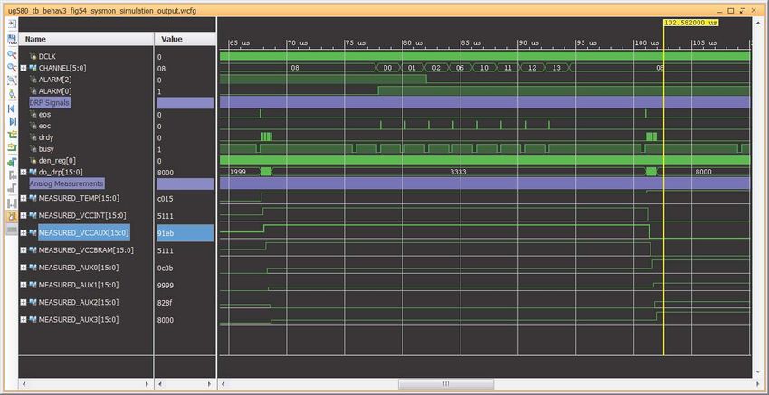
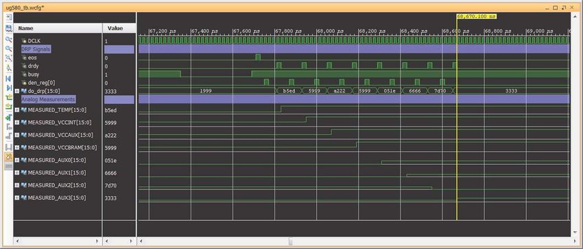
Example Design Test Bench . . . . . . . . . . . . . . . . . . . . . . . . . . . . . . . . . . . . . . . . . . . . . . 88
Simulation Output . . . . . . . . . . . . . . . . . . . . . . . . . . . . . . . . . . . . . . . . . . . . . . . . . . . . . 89
XADC User Guide www.xilinx.com 9
Send Feedback
UG480 (v1.10.1) July 23, 201810 www.xilinx.com XADC User Guide
Send Feedback
UG480 (v1.10.1) July 23, 2018Preface
About This Guide
Xilinx® 7 series FPGAs include four FPGA families that are all designed for lowest power
to enable a common design to scale across families for optimal power, performance, and
cost. The Spartan®-7 family is the lowest density with the lowest cost entry point into the
7 series portfolio. The Artix®-7 family is optimized for highest performance-per-watt and
bandwidth-per-watt for cost-sensitive, high volume applications. The Kintex®-7 family is
an innovative class of FPGAs optimized for the best price-performance. The Virtex®-7
family is optimized for highest system performance and capacity. The Zynq®-7000 SoC
device integrates a feature-rich dual-core Arm® Cortex™-A9 based processing system (PS)
and 28 nm Xilinx programmable logic (PL) in a single device.
This guide serves as a technical reference describing the 7 series FPGAs and Zynq-7000
SoC XADC, a dual 12-bit, 1 MSPS analog-to-digital converter with on-chip sensors. This
user guide is part of an overall set of documentation on the 7 series FPGAs and Zynq-7000
SoC devices, which is available on the Xilinx website at
www.xilinx.com/documentation.
Guide Contents
This manual contains these chapters:
• Chapter 1, Introduction and Quick Start
• Chapter 2, Analog-to-Digital Converter
• Chapter 3, XADC Register Interface
• Chapter 4, XADC Operating Modes
• Chapter 5, XADC Timing
• Chapter 6, Application Guidelines
Additional Resources
To find additional Xilinx documentation, see the Xilinx website at:
www.xilinx.com/support/documentation/index
To search the Answer Database of silicon, software, and IP questions and answers, see the
Xilinx website at:
www.xilinx.com/support
To find Xilinx Analog Mixed Signal (AMS) information, see the Xilinx website at:
www.xilinx.com/ams
XADC User Guide www.xilinx.com 11
Send Feedback
UG480 (v1.10.1) July 23, 2018Preface: About This Guide
Example design files and Tcl console examples for the Vivado® Hardware Manager can be
found in the ZIP file that accompanies this user guide:
References
Additional material useful to this document can be found here:
1. (PG019), LogiCORE IP AXI XADC (v1.0) Product Guide
2. (UG475), 7 Series FPGAs Packaging and Pinout Product Specifications User Guide
3. (UG470), 7 Series FPGAs Configuration User Guide
4. (UG585), Zynq-7000 SoC Technical Reference Manual
5. (PG091), XADC Wizard LogiCORE IP Product Guide for Vivado Design Suite
6. (XAPP554), XADC Layout Guidelines Application Note
7. (XAPP795), Driving the Xilinx Analog-to-Digital Converter Application Note
8. (UG908), Vivado Design Suite User Guide: Programming and Debugging
9. (WP442), Efficient Implementation of Analog Signal Processing Functions in Xilinx Devices
10. (UG865), Zynq-7000 SoC Packaging and Pinout Product Specification User Guide
11. (DS180), 7 Series FPGAs Overview
12 www.xilinx.com XADC User Guide
Send Feedback
UG480 (v1.10.1) July 23, 2018Chapter 1
Introduction and Quick Start
This chapter provides a brief overview of the Xilinx 7 series FPGAs XADC functionality.
The XADC is available in all Artix®-7, Kintex®-7, Virtex®-7, and Zynq®-7000 SoC devices.
The XADC is also available in many, but not all Spartan®-7 devices. To identify specific
devices that support the XADC block, consult the Spartan-7 family overview in DS180,
7 Series FPGAs Overview [Ref 11].
The XADC is the basic building block that enables analog mixed signal (AMS)
functionality which is new to 7 series FPGAs. By combining high quality analog blocks
with the flexibility of programmable logic, it is possible to craft customized analog
interfaces for a wide range of applications. See www.xilinx.com/ams for more
information.
This chapter contains only key information to allow a basic understanding of the XADC
block. With this introduction, you can learn the pinout requirements and determine how to
instantiate basic functionality in their designs. Subsequent chapters provide more detailed
descriptions of the XADC functionality.
XADC Overview
The XADC includes a dual 12-bit, 1 Mega sample per second (MSPS) ADC and on-chip
sensors. The ADCs and sensors are fully tested and specified (see the respective 7 series
FPGAs data sheet). The ADCs provide a general-purpose, high-precision analog interface
for a range of applications. Figure 1-1 shows a block diagram of the XADC. The dual ADCs
support a range of operating modes, for example, externally triggered and simultaneous
sampling on both ADCs (see Chapter 4, XADC Operating Modes) and various analog
input signal types, for example, unipolar and differential (see Chapter 2, Analog-to-Digital
Converter). The ADCs can access up to 17 external analog input channels.
XADC User Guide www.xilinx.com 13
Send Feedback
UG480 (v1.10.1) July 23, 2018Chapter 1: Introduction and Quick Start
X-Ref Target - Figure 1-1
VREP_0 VREFN_0
Temperature Supply
VCCINT
Sensor Sensors VCCAUX
VCCBRAM
Die VCCPINT(1)
°C On-Chip Ref
Temperature VCCPAUX(1)
VCCO_DDR(1) 1.25V
Control Status
VP_0 12-bit, Registers Registers
VN_0 Mux 1 MSPS
VAUXP[0] ADC A
VAUXN[0]
64 x 16 bits 64 x 16 bits
Read/Write Read Only
VAUXP[12]
VAUXN[12] Mux
VAUXP[13] 12-bit,
External
VAUXN[13] 1 MSPS
Analog
VAUXP[14] ADC B
Inputs
VAUXN[14]
VAUXP[15]
VAUXN[15]
DRP
FPGA
JTAG
Interconnect
X17015-110817
Figure 1-1: XADC Block Diagram
Notes relevant to Figure 1-1:
1. Zynq-7000 SoC devices only.
The XADC also includes several on-chip sensors that support measurement of the on-chip
power supply voltages and die temperature. The ADC conversion data is stored in
dedicated registers called status registers. These registers are accessible through the FPGA
interconnect using a 16-bit synchronous read and write port called the dynamic
reconfiguration port (DRP). ADC conversion data is also accessible through the JTAG TAP,
either before (pre-configuration) or after configuration. For JTAG TAP, users are not
required to instantiate the XADC because it is a dedicated interface that uses the existing
FPGA JTAG infrastructure. As discussed later, if the XADC is not instantiated in a design,
the device operates in a predefined mode (called default mode) that monitors on-chip
temperature and supply voltages.
XADC operation is user defined by writing to the control registers using either the DRP or
JTAG interface. It is also possible to initialize these register contents when the XADC is
instantiated in a design using the block attributes.
Differences between Virtex-5 and Virtex-6 System Monitors
For Virtex®-5 and Virtex®-6 FPGA System Monitor users, the XADC functionality is fully
backward compatible with legacy System Monitor designs. The XADC functionality and
interface are familiar to those who have previously designed with the System Monitor.
System Monitor designs are automatically retargeted to the XADC site by the software
tools.
However, the XADC block in 7 series FPGAs contains a large number of new features and
enhancements detailed in subsequent chapters. The new functionality is enabled by
14 www.xilinx.com XADC User Guide
Send Feedback
UG480 (v1.10.1) July 23, 2018XADC Pinout Requirements
initializing previously undefined status registers and bit locations. Old System Monitor
designs that did not initialize these new registers or bit locations behave exactly the same
way as before.
XADC Pinout Requirements
Dedicated Package Pins
All XADC dedicated pins are located in bank 0 and thus have the _0 suffix in the package
file names. Figure 1-2 shows the basic pinout requirements for the XADC. There are two
recommended configurations. On the left, the XADC is powered from VCCAUX (1.8V) and
uses an external 1.25V reference source. The external reference delivers the best
performance in terms of accuracy and thermal drift. A ferrite bead is used to isolate the
ground reference for the analog circuits and system ground. An additional low-pass filter
for VCCAUX supply will similarly improve the ADC performance. See Chapter 6,
Application Guidelines for more information. Shared or common ground impedance is the
most common way to introduce unwanted noise into analog circuits.
X-Ref Target - Figure 1-2
Use External Reference IC Enable On-Chip Reference
VCCAUX (1.8V ± 5%) VCCAUX (1.8V ± 5%)
1.8V – 5V Filter VCCAUX Supply Filter VCCAUX Supply
1.25V + 0.2%
50 ppm/°C 100 nF
VREFP VCCADC VREFP VCCADC
VP VP
100 nF 470 nF 100 nF 470 nF
ADC ADC
10 μF VN VN
VREFN GNDADC VREFN GNDADC
Ferrite bead for high frequency Ferrite bead for high frequency
GND GND
noise isolation noise isolation
Package Pins
X17016-072318
Figure 1-2: XADC Pinout Requirements
It is also possible to use an on-chip reference for the ADCs. To enable the on-chip reference
source, the VREFP pin must be connected to ground as shown on the right of Figure 1-2.
Where only basic on-chip thermal and supply monitoring is required, using the on-chip
reference provides good performance. Users should consult the respective data sheet to see
the accuracy specifications when using the external and on-chip reference sources.
Table 1-1 lists the pins associated with the XADC and the recommended connectivity.
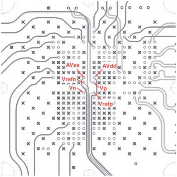
Note: It is also important to place the 100 nF decoupling capacitors as close as possible to the
package balls to minimize inductance between the decoupling and package balls.
XADC User Guide www.xilinx.com 15
Send Feedback
UG480 (v1.10.1) July 23, 2018Chapter 1: Introduction and Quick Start
Table 1-1: XADC Package Pins
Package Pin Type Description
This is the analog supply pin for the ADCs and other analog circuits in the
XADC. It can be tied to the 1.8V VCCAUX supply; however, in a mixed-signal
system, the supply should be connected to a separate 1.8V analog, if available.
VCCADC_0 Power supply
See Analog Power Supply and Ground (VCCADC and GNDADC), page 77 for
more information. This pin should never be tied to GND. The pin should be
tied to VCCAUX even if the XADC is not being used.
This is the ground reference pin for the ADCs and other analog circuits in the
XADC. It can be tied to the system ground through an isolating ferrite bead as
shown in Figure 1-2. In a mixed-signal system this pin should be tied to an
GNDADC_0 Power supply analog ground plane if available, in which case the ferrite bean is not required.
See Analog Power Supply and Ground (VCCADC and GNDADC), page 77 for
more information. This pin should always be tied to GND even if the XADC is
not being used.
This pin can be tied to an external 1.25V accurate reference IC (±0.2% or
±9 LSBs at 12 bits) for best performance of the ADCs. It should be treated as an
analog signal that together with the VREFN signal provides a differential 1.25V
Reference voltage
VREFP_0 voltage. By connecting this pin to GNDADC (see Figure 1-2), an on-chip
input
reference source (±1% or ±41 LSBs at 12 bits) is activated. This pin should
always be connected to GNDADC if an external reference is not supplied. See
Reference Inputs (VREFP and VREFN), page 77 for more information.
This pin should be tied to the GND pin of an external 1.25V accurate reference
IC (±0.2%) for best performance of the ADCs. It should be treated as an analog
Reference voltage signal that together with the VREFP signal provides a differential 1.25V
VREFN_0
input voltage. This pin should always be connected to GND even if an external
reference is not supplied. See Reference Inputs (VREFP and VREFN), page 77 for
more information.
This is the positive input terminal of the dedicated differential analog input
Dedicated analog channel (VP/VN). The analog input channels are very flexible and support
VP_0
input multiple analog input signal types. For more information, see Analog Inputs,
page 28. This pin should be connected to GND if not used.
This is the negative input terminal of the dedicated differential analog input
Dedicated analog channel (VP/VN). The analog input channels are very flexible and support
VN_0
input multiple analog input signal types. For more information, see Analog Inputs,
page 28. This pin should be connected to GND if not used.
These are multi-function pins that can support analog inputs or can be used as
regular digital I/O (see Figure 1-1). These pins support up to 16 positive input
Auxiliary analog terminals of the differential auxiliary analog input channels (VAUXP/VAUXN).
_AD0P_ to
inputs/digital The analog input channels are very flexible and support multiple analog input
_AD15P_(1)(2)
I/O signal types. For more information, see Analog Inputs, page 28. When not
being used as analog inputs, these pins can be treated like any other digital
I/O.
16 www.xilinx.com XADC User Guide
Send Feedback
UG480 (v1.10.1) July 23, 2018XADC Pinout Requirements
Table 1-1: XADC Package Pins (Cont’d)
Package Pin Type Description
These are multi-function pins that can support analog inputs or can be used
as regular digital I/O (see Figure 1-1). These pins support up to 16 negative
Auxiliary analog input terminals of the differential auxiliary analog input channels
_AD0N_ to
inputs/digital (VAUXP/VAUXN). The analog input channels are very flexible and support
_AD15N_(1) (2)
I/O multiple analog input signal types. For more information, see Analog Inputs,
page 28. When not being used as analog inputs, these pins can be treated like
any other digital I/O.
Notes:
1. FPGA I/Os that are analog input-enabled contain the _ADxP_ and _ADxN_ designation in the package file name, for example,
IO_L1P_T0_AD0P_35 is the input pin for analog auxiliary channel VAUXP[0]. IO_L1N_T0_AD0N_35 is the input pin for analog
auxiliary channel VAUXN[0]. For more information, see UG475, 7 Series FPGAs Packaging and Pinout Product Specifications User Guide
[Ref 2].
2. Auxiliary channels 6, 7, 13, 14, and 15 are not supported in Kintex-7 devices. Some auxiliary analog channels might also not be
supported in certain Virtex-7, Artix-7, Spartan-7, and Zynq-7000 SoC device package options. You should consult the package file for
the device.
Note: Chapter 6, Application Guidelines, should be consulted before commencing any PC board
layout. Board layout and external component choices can greatly impact the performance of the
ADCs.
External Analog Inputs
Apart from a single dedicated analog input pair (VP/VN), the external analog inputs use
dual-purpose I/O. These FPGA digital I/Os are individually nominated as analog inputs
when the XADC is instantiated in a design. This document refers to these analog inputs as
auxiliary analog inputs. A maximum of 16 auxiliary analog inputs are available. The
auxiliary analog inputs are enabled by connecting the analog inputs on the XADC
primitive to the top level of the design. When enabled as analog inputs, these package balls
are unavailable as digital I/Os. It is also possible to enable the auxiliary analog inputs
preconfiguration (for example, for PCB diagnostics) through the JTAG TAP (see JTAG DRP
Commands for more information.)
All analog input channels are differential and require two package balls. Typically, the
auxiliary analog inputs are allocated evenly over banks 15 and 35. However, users should
consult the pinout information in UG475, 7 Series FPGAs Packaging and Pinout Product
Specifications User Guide [Ref 2] for a particular device and package combination.
Analog-capable I/O have the ADxP or ADxN suffix on the I/O name in the package files.
For example, auxiliary analog input channel 8 has associated package ball names ending
with AD8P and AD8N. See UG475, 7 Series FPGAs Packaging and Pinout Product
Specifications User Guide [Ref 2] for more information. The auxiliary analog inputs have a
fixed package ball assignment and cannot be moved.
Auxiliary analog inputs are supported differently in Vivado® tools when compared to ISE
tools. The auxiliary analog inputs do not require any user-specified constraints or pin
locations in ISE tools. ISE external auxiliary inputs do not need an I/O standard setting to
be added to your constraints file (UCF) or in the PlanAhead™ design tool. In Vivado
design tools, the auxiliary analog inputs must be assigned to the associated pin location.
XADC User Guide www.xilinx.com 17
Send Feedback
UG480 (v1.10.1) July 23, 2018Chapter 1: Introduction and Quick Start
Auxiliary analog inputs must be connected to the top level of the design.
Note: Auxiliary channels 6, 7, 13, 14, and 15 are not supported on Kintex-7 devices. Some auxiliary
analog channels might also not be supported in certain Virtex-7, Artix-7, Spartan-7, and Zynq-7000
SoC device package options. Users should consult the package file for the device.
Instantiating the XADC
As mentioned previously, it is not necessary to instantiate the XADC in a design to access
the on-chip monitoring capability. However, if the XADC is not instantiated in a design,
the only way to access this information is through the JTAG test access port (TAP). To allow
access to the status registers (measurement results) from the FPGA logic, the XADC must
be instantiated. These subsections give a brief overview of the XADC primitive (ports and
attributes).
XADC Ports
Figure 1-3 shows the ports on the XADC primitive, and Table 1-2 describes the
functionality of the ports.
X-Ref Target - Figure 1-3
XADC
DO[15:0]
DI[15:0]
Dynamic DADDR[6:0]
Reconfiguration Port DEN
(DRP)
DWE
ALM[7:0]
DCLK ALARMS
OT
DRDY
RESET MUXADDR[4:0]
CONTROL
and CLOCK CONVST CHANNEL[4:0]
CONVSTCLK EOC
EOS
STATUS
BUSY
VP JTAGLOCKED
VN JTAGMODIFIED
External
Analog VAUXP[15:0] JTAGBUSY
Inputs
VAUXN[15:0]
X17017-110817
Figure 1-3: XADC Primitive Ports
18 www.xilinx.com XADC User Guide
Send Feedback
UG480 (v1.10.1) July 23, 2018Instantiating the XADC
Table 1-2: XADC Port Descriptions
Port I/O Description
DI[15:0] Inputs Input data bus for the DRP.(1)
DO[15:0] Outputs Output data bus for the DRP.(1)
DADDR[6:0] Input Address bus for the DRP.(1)
DEN(2) Input Enable signal for the DRP.(1)
DWE(2) Input Write enable for the DRP.(1)
DCLK Input Clock input for the DRP.(1)
DRDY(2) Output Data ready signal for the DRP.(1)
Asynchronous reset signal for the XADC control logic.
RESET(2) Input RESET will be deasserted synchronously to DCLK or the
internal configuration clock when DCLK is stopped.
Convert start input. This input controls the sampling
instant on the ADC(s) inputs and is only used in event
CONVST(3) Input mode timing (see Event-Driven Sampling, page 73). This
input comes from the general-purpose interconnect in the
FPGA logic.
Convert start clock input. This input is connected to a clock
net. Like CONVST, this input controls the sampling instant
on the ADC(s) inputs and is only used in event mode
CONVSTCLK(3) Input timing. This input comes from the local clock distribution
network in the FPGA logic. Thus, for the best control over
the sampling instant (delay and jitter), a global clock input
can be used as the CONVST source.
One dedicated analog input pair. The XADC has one pair of
dedicated analog input pins that provide a differential
VP , VN Input analog input. When designing with the XADC feature but
not using the dedicated external channel of VP and VN, you
should connect both VP and VN to analog ground.
Sixteen auxiliary analog input pairs. In addition to the
dedicated differential analog input, the XADC can access
VAUXP[15:0], 16 differential analog inputs by configuring digital I/O as
Inputs
VAUXN[15:0] analog inputs. These inputs can also be enabled
pre-configuration through the JTAG port (see DRP JTAG
Interface, page 47).
ALM[0](2) Output Temperature sensor alarm output.
(2)
ALM[1] Output VCCINT sensor alarm output.
ALM[2](2) Output VCCAUX sensor alarm output.
ALM[3](2) Output VCCBRAM sensor alarm output.
ALM[4](4) Output VCCPINT sensor alarm output.
ALM[5](4) Output VCCPAUX sensor alarm output.
(4)
ALM[6] Output VCCO_DDR sensor alarm output.
XADC User Guide www.xilinx.com 19
Send Feedback
UG480 (v1.10.1) July 23, 2018Chapter 1: Introduction and Quick Start
Table 1-2: XADC Port Descriptions (Cont’d)
Port I/O Description
Logic OR of bus ALM[6:0]. Can be used to flag the
ALM[7](2) Output
occurrence of any alarm.
OT(2) Output Over-Temperature alarm output.
These outputs are used in external multiplexer mode. They
indicate the address of the next channel in a sequence to be
MUXADDR[4:0] Outputs converted. They provide the channel address for an
external multiplexer (see External Multiplexer Mode,
page 63).
Channel selection outputs. The ADC input MUX channel
CHANNEL[4:0] Outputs selection for the current ADC conversion is placed on these
outputs at the end of an ADC conversion.
End of conversion signal. This signal transitions to
(2) active-High at the end of an ADC conversion when the
EOC Output
measurement is written to the status registers (see
Chapter 5, XADC Timing).
End of sequence. This signal transitions to active-High
(2) when the measurement data from the last channel in an
EOS Output
automatic channel sequence is written to the status
registers (see Chapter 5, XADC Timing).
ADC busy signal. This signal transitions High during an
BUSY(2) Output ADC conversion. This signal also transitions High for an
extended period during an ADC or sensor calibration.
Indicates that a DRP port lock request has been made by the
(2) JTAG interface (see DRP JTAG Interface, page 47). This
JTAGLOCKED Output
signal is also used to indicate that the DRP is ready for
access (when Low).
JTAGMODIFIED(2) Output Used to indicate that a JTAG write to the DRP has occurred.
JTAGBUSY(2) Output Used to indicate that a JTAG DRP transaction is in progress.
Notes:
1. The DRP is the interface between the XADC and FPGA. All XADC registers can be accessed from the
FPGA logic using this interface. For more details on the timing for these DRP signals, see Figure 5-3,
page 75.
2. Active-High signal.
3. Rising edge triggered signal.
4. Only available on Zynq-7000 SoC devices.
20 www.xilinx.com XADC User Guide
Send Feedback
UG480 (v1.10.1) July 23, 2018Instantiating the XADC
XADC Attributes
The block diagram in Figure 1-1 shows the control registers that define the operation of the
XADC. The control registers are a set of 32 16-bit registers. As mentioned, these registers
can be read and written through the DRP or JTAG ports. It is also possible to initialize the
contents of these registers during the configuration of the FPGA. This enables the XADC to
start operating in a user-defined mode after configuration is complete. There are
32 attributes associated with the XADC primitive that allow users to initialize these
registers. Table 1-3 lists these attributes. The attributes are called INIT_xx, where xx
corresponds to the hexadecimal address of the register on the DRP. For example, INIT_40
corresponds to the first control register at address 40h on the DRP.
Table 1-3: XADC Primitive Attributes
Control Register
Attribute Name Description
Address
Configuration XADC configuration registers (see
INIT_40 40h
register 0 Control Registers, page 42).
Configuration
INIT_41 41h
register 1
Configuration
INIT_42 42h
register 2
XADC Test registers for factory use
INIT_43 to
Test registers 43h to 47h only. The default initialization is
INIT_47
0000h.
Sequence registers used to program
INIT_48 to Sequence the XADC Channel Sequencer
48h to 4Fh
INIT_4F registers function (see Automatic Channel
Sequencer, page 55).
Alarm threshold registers for the
INIT_50 to Alarm limit
50h to 5Fh XADC alarm function (see
INIT_5F registers
Automatic Alarms, page 65).
The XADC primitive also has an attribute called SIM_MONITOR_FILE that points to the
analog stimulus file. This attribute is required to support simulation. This attribute points
to the path and file name of a text file that contains analog information (for example,
temperature and voltage). UNISIM and SIMPRIM models use this text file during
simulation. This is the only way analog signals can be introduced into a simulation of the
XADC. For more information see XADC Software Support, page 82.
Example Instantiation
Instantiating the XADC involves connecting the required I/O (including analog inputs) to
the design and optionally initializing the control registers to define the XADC operation
after configuration. Alternatively, users can write to the control registers through the DRP
after device configuration. The timing diagram for DRP read and write operations is
shown in Figure 5-3.
Note: The read/write operation is not valid or complete until the DRDY signal goes active.
This subsection provides a brief example of an XADC instantiation using Verilog. First, the
control registers are initialized, and then the required XADC I/Os are connected to the
design. The software correctly ties off unconnected I/Os on the primitive.
XADC User Guide www.xilinx.com 21
Send Feedback
UG480 (v1.10.1) July 23, 2018Chapter 1: Introduction and Quick Start
This design assumes an external 50 MHz clock is used for DCLK, and the XADC is
configured to monitor temperature, supply voltages, and activate alarms if safe limits are
exceeded. This example is explained in detail in XADC Software Support, page 82.
XADC #(
// Initializing the XADC Control Registers
.INIT_40(16'h9000),// Calibration coefficient averaging disabled
// averaging of 16 selected for external channels
.INIT_41(16'h2ef0),// Continuous Sequencer Mode, Disable unused ALMs,
// Enable calibration
.INIT_42(16'h0400),// Set DCLK divider to 4, ADC = 500Ksps, DCLK = 50MHz
.INIT_48(16'h4701),// Sequencer channel - enable Temp sensor, VCCINT, VCCAUX,
// VCCBRAM, and calibration
.INIT_49(16'h000f),// Sequencer channel - enable aux analog channels 0 - 3
.INIT_4A(16'h4700),// Averaging enabled for Temp sensor, VCCINT, VCCAUX,
// VCCBRAM
.INIT_4B(16'h0000),// No averaging on external channels
.INIT_4C(16'h0000),// Sequencer Bipolar selection
.INIT_4D(16'h0000),// Sequencer Bipolar selection
.INIT_4E(16'h0000),// Sequencer Acq time selection
.INIT_4F(16'h0000),// Sequencer Acq time selection
.INIT_50(16'hb5ed),// Temp upper alarm trigger 85°C
.INIT_51(16'h5999),// Vccint upper alarm limit 1.05V
.INIT_52(16'hA147),// Vccaux upper alarm limit 1.89V
.INIT_53(16'h0000),// OT upper alarm limit 125°C using automatic shutdown
.INIT_54(16'ha93a),// Temp lower alarm reset 60°C
.INIT_55(16'h5111),// Vccint lower alarm limit 0.95V
.INIT_56(16'h91Eb),// Vccaux lower alarm limit 1.71V
.INIT_57(16'hae4e),// OT lower alarm reset 70°C
.INIT_58(16'h5999),// VCCBRAM upper alarm limit 1.05V
.INIT_5C(16'h5111),// VCCBRAM lower alarm limit 0.95V
.SIM_MONITOR_FILE("sensor_input.txt")
// Analog Stimulus file. Analog input values for simulation
)
XADC_INST ( // Connect up instance IO. See UG480 for port descriptions
.CONVST(GND_BIT), // not used
.CONVSTCLK(GND_BIT), // not used
.DADDR(DADDR_IN[6:0]),
.DCLK(DCLK_IN),
.DEN(DEN_IN),
.DI(DI_IN[15:0]),
.DWE(DWE_IN),
.RESET(RESET_IN),
.VAUXN(aux_channel_n[15:0]),
.VAUXP(aux_channel_p[15:0]),
.ALM(alm_int),
.BUSY(BUSY_OUT),
.CHANNEL(CHANNEL_OUT[4:0]),
.DO(DO_OUT[15:0]),
.DRDY(DRDY_OUT),
.EOC(EOC_OUT),
.EOS(EOS_OUT),
.JTAGBUSY(),// not used
.JTAGLOCKED(),// not used
.JTAGMODIFIED(),// not used
.OT(OT_OUT),
.MUXADDR(),// not used
.VP(VP_IN),
.VN(VN_IN)
);
22 www.xilinx.com XADC User Guide
Send Feedback
UG480 (v1.10.1) July 23, 2018Instantiating the XADC
ADC and Sensors
More comprehensive information regarding the operation of the ADCs and on-chip
sensors can be found in Chapter 2, Analog-to-Digital Converter. This section provides a
brief overview to help users to quickly interpret data read from the status registers and
verify the operation of the XADC.
Analog-to-Digital Converter
The ADCs have a nominal analog input range from 0V to 1V. In unipolar mode (default),
the analog inputs of the ADCs produce a full scale code of FFFh (12 bits) when the input is
1V. Thus, an analog input signal of 200 mV in unipolar mode produces and outputs code of
Equation 1-1.
( ( 0.2 ⁄ 1.0 ) × FFFh ) = 819 or 333h Equation 1-1
In bipolar mode, the ADCs use two’s complement coding and produces a full scale code of
7FFh with +0.5V input and 800h with –0.5V input.
Temperature Sensor
The temperature sensor has a transfer function given by Equation 1-2.
ADC Code × 503.975
Temp ( °C ) = ------------------------------------------------------ – 273.15 Equation 1-2
4096
For example, ADC Code 2423 (977h) = 25°C.
The temperature sensor result can be found in status register 00h.
Power Supply Sensors
The XADC power supply sensors have a transfer function that generates a full scale ADC
output code of FFFh with a 3V input voltage. This voltage is outside the allowed supply
range, but the FPGA supply measurements map into this measurement range. Thus,
VCCINT = 1V generates an output code of 1/3 x 4096 = 1365 = 555h. The XADC monitors
VCCINT, VCCAUX, and VCCBRAM. The measurement results are stored in status registers
01h, 02h, and 06h, respectively.
Zynq-7000 SoC
The XADC monitors three additional power supplies on the Zynq-7000 SoC devices. The
supplies are VCCPINT, VCCPAUX, and VCCO_DDR. These measurements are stored in status
registers 0Dh, 0Eh, and 0Fh, respectively.
XADC User Guide www.xilinx.com 23
Send Feedback
UG480 (v1.10.1) July 23, 2018Chapter 1: Introduction and Quick Start
24 www.xilinx.com XADC User Guide
Send Feedback
UG480 (v1.10.1) July 23, 2018Chapter 2
Analog-to-Digital Converter
The XADC block contains two 12-bit, 1 MSPS ADCs. These ADCs are available for use
with both external analog inputs and on-chip sensors. Several predefined operating modes
are available that cover the most typical use cases for these ADCs. The various operating
modes are covered in Chapter 4, XADC Operating Modes. This chapter focuses on the
detailed operation of the ADC and the on-chip sensors. The various input configurations
for the external analog inputs are also covered. All operating modes of the ADC, sensors,
and analog inputs are configured using the XADC control registers. A detailed description
of the control registers is covered in Chapter 3, XADC Register Interface.
ADC Transfer Functions
The ADCs have transfer functions as shown in Figure 2-2 and Figure 2-3. These transfer
functions reflect unipolar and bipolar operating modes, respectively. All on-chip sensors
use the unipolar mode of operation for the ADC. Users can optionally configure the
external analog input channels to operate in unipolar or bipolar modes (see Analog Inputs,
page 28).
For the ADCs to function as specified, the power supplies and reference options must be
configured correctly. The required package ball connections are shown in Figure 1-2. Other
important aspects to ensure optimal ADC performance are the PCB layout and external
component selection. These issues are covered in Chapter 6, Application Guidelines. It is
recommended that you read this chapter is before the board design is started.
X-Ref Target - Figure 2-1
DI15 DI14 DI13 DI12 DI11 DI10 DI9 DI8 DI7 DI6 DI5 DI4 DI3 DI2 DI1 DI0
Status Registers
DATA[11:0] Note DADDR[6:0] = (00h-07h, 10h-2Fh)
X17018-110817
Figure 2-1: Status Registers
Note: The ADCs always produce a 16-bit conversion result. The 12-bit data correspond to the 12
MSBs (most significant) in the 16-bit status registers. The unreferenced LSBs can be used to
minimize quantization effects or improve resolution through averaging or filtering. See Figure 2-1.
XADC User Guide www.xilinx.com 25
Send Feedback
UG480 (v1.10.1) July 23, 2018Chapter 2: Analog-to-Digital Converter
Unipolar Mode
Figure 2-2 shows the 12-bit unipolar transfer function for the ADCs. The nominal analog
input range to the ADCs is 0V to 1V in this mode. The ADC produces a zero code (000h)
when 0V is present on the ADC input and a full scale code of all 1s (FFFh) when 1V is
present on the input.
The ADC output coding in unipolar mode is straight binary. The designed code transitions
occur at successive integer LSB values such as one LSB, two LSBs, and three LSBs, etc. The
LSB size in volts is equal to 1V/212 or 1V/4096 = 244 µV. The analog input channels are
differential in nature and require both the positive (VP) and negative (VN) inputs of the
differential input to be driven. More details on the analog inputs and the kinds of inputs
signals that can be accommodated are covered in the Analog Inputs section.
X-Ref Target - Figure 2-2
Output Code Full Scale
Transition
FFF
FFE Full Scale Input = 1V1
LSB = 1V / 4096 = 244 μV
FFD
12-Bit Output Code (Hex)
004
003
002
001
000
44
+0 8
32
5
8
.7
.2
.4
.7
99
+0
+0
+9
Input Voltage (mV)
X17064-110817
Figure 2-2: Unipolar Transfer Function
26 www.xilinx.com XADC User Guide
Send Feedback
UG480 (v1.10.1) July 23, 2018ADC Transfer Functions
Bipolar Mode
When the external analog input channels of the ADCs are configured as bipolar, they can
accommodate true differential and bipolar analog signal types (see the Analog Inputs
section). When dealing with differential signal types, it is useful to have both sign and
magnitude information about the analog input signal. Figure 2-3 shows the ideal transfer
function for bipolar mode operation. The output coding of the ADC in bipolar mode is
two’s complement and is intended to indicate the sign of the input signal on VP relative to
VN. The designed code transitions occur at successive integer LSB values, that is, one LSB,
two LSBs, three LSBs, etc. The LSB size in volts is equal to 1V/212 or 1V/4096 = 244 µV.
X-Ref Target - Figure 2-3
Output Code
(Two’s Complement Coding)
7FFh Full Scale Input = 1V
7FEh 1 LSB = 1V / 4096 = 244 μV
002h
12-Bit Output Code (Hex)
001h
000h
FFFh
FFEh
FFDh
801h
800h
5
44
+0 4
88
88
00
.7
4
0
.2
.2
.4
99
.4
-5
-0
+0
-0
+4
Input Voltage (mV)
X17019-110817
Figure 2-3: Bipolar Transfer Function
XADC User Guide www.xilinx.com 27
Send Feedback
UG480 (v1.10.1) July 23, 2018Chapter 2: Analog-to-Digital Converter
Analog Inputs
The analog inputs of the ADC use a differential sampling scheme to reduce the effects of
common-mode noise signals. This common-mode rejection improves the ADC
performance in noisy digital environments. Figure 2-4 shows the benefits of a differential
sampling scheme. Common ground impedances (RG) couple noise voltages (switching
digital currents) into other parts of a system. These noise signals can be 100 mV or more.
For the ADCs, this noise voltage is equivalent to hundreds of LSBs, thus inducing large
measurement errors. The differential sampling scheme samples both the signal and any
common mode noise voltages at both analog inputs (VP and VN). The common mode
signal is effectively subtracted because the Track-and-Hold amplifier captures the
difference between VP and VN or VP minus VN. To take advantage of the high common
mode rejection, users need only connect VP and VN in a differential configuration.
X-Ref Target - Figure 2-4
Differential
Sampling
VP
+
Noise
T/H
Current –
VN
Noise
Voltage
R G (1)
Common Noise Common Mode
on VP and VN Rejection removes
1V 1V
noise VP – VN
VP
VN
0V 0V
Note 1: RG is Common Ground Impedance. X17020-110817
Figure 2-4: Common Mode Noise Rejection
28 www.xilinx.com XADC User Guide
Send Feedback
UG480 (v1.10.1) July 23, 2018Analog Inputs
Auxiliary Analog Inputs
The auxiliary analog inputs (VAUXP[15:0] and VAUXN[15:0]) are analog inputs that are
shared with regular digital I/O package balls. The auxiliary analog inputs are
automatically enabled when the XADC is instantiated in a design, and these inputs are
connected on the top level of the design. The auxiliary analog inputs do not require any
user-specified constraints or pin locations. They do not require an I/O standard setting to
be added to the UCF or in the PlanAhead pinout tool. In the Vivado design tools, an
IOSTANDARD must be selected that is compatible for the bank even though the
IOSTANDARD does not affect the input programming. All configuration is automatic
when the analog inputs are connected to the top level of the design. Only those auxiliary
inputs connected in a design are enabled as analog inputs. The XADC auxiliary inputs pins
are labeled in UG475, 7 Series FPGAs Packaging and Pinout Product Specifications User Guide
[Ref 2] by appending _ADxP_ and _ADxN_ to the I/O name, where x is the auxiliary pair
number. For example, the auxiliary input VAUXP[15] could be designated
IO_LxxP_xx_AD15P_xx in the pinout specification.
When designated as analog inputs, these inputs are unavailable for use as digital I/Os. If
the I/O is used as a digital I/O, it is subject to the specifications of the configured I/O
standard. If the I/O is used as an analog input, the input voltage must adhere to the
specifications given in the “Analog-to-Digital Converter” section of the respective data
sheet.
It is possible to enable any number of auxiliary analog inputs in an I/O bank and use the
remaining as digital I/Os. If there is a mixture of analog and digital I/Os in a bank, the I/O
bank must be powered by a supply required to meet the specifications of the digital I/O
standard in used. The analog input signal should not exceed the I/O bank supply voltage
(VCCO) in this case.
Note: Auxiliary channels 6, 7, 13, 14, and 15 are not supported on Kintex-7 devices. Some auxiliary
analog channels might also not be supported in certain Virtex-7, Artix-7, Spartan-7, and Zynq-7000
SoC device package options. Users should consult the package file for the device.
Adjusting the Acquisition Settling Time
The maximum conversion rate specified for the ADC is 1 MSPS or a conversion time of
1 µs. In continuous sampling mode (see Chapter 5, XADC Timing), 26 ADCCLK cycles are
required to acquire an analog signal and perform a conversion. This implies a maximum
ADCCLK frequency of 26 MHz. If the ACQ bit has not been set, four ADCCLKs or 150 ns
is allowed for the final stages of the acquisition. When using single channel mode, the ACQ
bit in configuration register 0[40h] (see Control Registers, page 42), or when using the
sequencer, the appropriate ACQ bit in the sequencer registers should be set (see ADC
Channel Settling Time (4Eh and 4Fh), page 58). This “settling” time ensures that the
analog input voltage is acquired to a 12-bit accuracy. The settling time can be increased by
reducing the ADCCLK frequency or setting the ACQ bit. In the latter case, assuming the 26
MHz maximum clock frequency, the settling time is increased to 380 ns (10 ADCCLK
cycles), and the conversion rate would be reduced to 812 kSPS for the same ADCCLK
frequency. In event timing mode (see Chapter 5, XADC Timing), you can initiate the
conversion cycle by using CONVST or CONVSTCLK, allowing more control over the
acquisition time, if required.
XADC User Guide www.xilinx.com 29
Send Feedback
UG480 (v1.10.1) July 23, 2018You can also read