AXI4-Stream Infrastructure IP Suite v2.2 - LogiCORE IP Product Guide Vivado Design Suite - Xilinx
←
→
Page content transcription
If your browser does not render page correctly, please read the page content below
AXI4-Stream
Infrastructure IP Suite
v2.2
LogiCORE IP Product Guide

Vivado Design Suite
PG085 April 4, 2018
Table of Contents
        IP Facts

        Chapter 1: Overview
           Overview of Features. . . . . . . . . . . . . . . . . . . . . . . . . . . . . . . . . . . . . . . . . . . . . . . . . . . . . . . . . . . . . . . 7
           System Requirements . . . . . . . . . . . . . . . . . . . . . . . . . . . . . . . . . . . . . . . . . . . . . . . . . . . . . . . . . . . . . . 9
           Licensing and Ordering Information . . . . . . . . . . . . . . . . . . . . . . . . . . . . . . . . . . . . . . . . . . . . . . . . . . . 9

        Chapter 2: Product Specification
           AXI4-Stream Infrastructure IP Suite Modules . . . . . . . . . . . . . . . . . . . . . . . . . . . . . . . . . . . . . . . . . .                           10
           Standards . . . . . . . . . . . . . . . . . . . . . . . . . . . . . . . . . . . . . . . . . . . . . . . . . . . . . . . . . . . . . . . . . . . . . . .   16
           Performance. . . . . . . . . . . . . . . . . . . . . . . . . . . . . . . . . . . . . . . . . . . . . . . . . . . . . . . . . . . . . . . . . . . . .      17
           Resource Utilization. . . . . . . . . . . . . . . . . . . . . . . . . . . . . . . . . . . . . . . . . . . . . . . . . . . . . . . . . . . . . . .         19
           Port Descriptions . . . . . . . . . . . . . . . . . . . . . . . . . . . . . . . . . . . . . . . . . . . . . . . . . . . . . . . . . . . . . . . . .       21
           Register Space . . . . . . . . . . . . . . . . . . . . . . . . . . . . . . . . . . . . . . . . . . . . . . . . . . . . . . . . . . . . . . . . . . .      26

        Chapter 3: Designing with the Core
           General Design Guidelines . . . . . . . . . . . . . . . . . . . . . . . . . . . . . . . . . . . . . . . . . . . . . . . . . . . . . . . . . 28
           Clocking. . . . . . . . . . . . . . . . . . . . . . . . . . . . . . . . . . . . . . . . . . . . . . . . . . . . . . . . . . . . . . . . . . . . . . . . . 29
           Resets . . . . . . . . . . . . . . . . . . . . . . . . . . . . . . . . . . . . . . . . . . . . . . . . . . . . . . . . . . . . . . . . . . . . . . . . . . 30

        Chapter 4: Design Flow Steps
           Customizing and Generating the Core . . . . . . . . . . . . . . . . . . . . . . . . . . . . . . . . . . . . . . . . . . . . . . . .                       31
           Constraining the Core . . . . . . . . . . . . . . . . . . . . . . . . . . . . . . . . . . . . . . . . . . . . . . . . . . . . . . . . . . . . .           65
           Simulation . . . . . . . . . . . . . . . . . . . . . . . . . . . . . . . . . . . . . . . . . . . . . . . . . . . . . . . . . . . . . . . . . . . . . .    67
           Synthesis and Implementation . . . . . . . . . . . . . . . . . . . . . . . . . . . . . . . . . . . . . . . . . . . . . . . . . . . . . .                  67

        Chapter 5: Example Design
           Functionality. . . . . . . . . . . . . . . . . . . . . . . . . . . . . . . . . . . . . . . . . . . . . . . . . . . . . . . . . . . . . . . . . . . . . 69

        Chapter 6: Test Bench

        Appendix A: Migrating and Upgrading
           Device Migration . . . . . . . . . . . . . . . . . . . . . . . . . . . . . . . . . . . . . . . . . . . . . . . . . . . . . . . . . . . . . . . . . 71

AXI4-Stream Infrastructure IP Suite v2.2                           www.xilinx.com                                                Send Feedback
                                                                                                                                                                     2
PG085 April 4, 2018
Migrating to the Vivado Design Suite. . . . . . . . . . . . . . . . . . . . . . . . . . . . . . . . . . . . . . . . . . . . . . . . . 71
Upgrading in the Vivado Design Suite . . . . . . . . . . . . . . . . . . . . . . . . . . . . . . . . . . . . . . . . . . . . . . . . 71
Appendix B: Debugging
Finding Help on Xilinx.com . . . . . . . . . . . . . . . . . . . . . . . . . . . . . . . . . . . . . . . . . . . . . . . . . . . . . . . . . 73
Debug Tools . . . . . . . . . . . . . . . . . . . . . . . . . . . . . . . . . . . . . . . . . . . . . . . . . . . . . . . . . . . . . . . . . . . . . 74
Hardware Debug . . . . . . . . . . . . . . . . . . . . . . . . . . . . . . . . . . . . . . . . . . . . . . . . . . . . . . . . . . . . . . . . . 75
Interface Debug . . . . . . . . . . . . . . . . . . . . . . . . . . . . . . . . . . . . . . . . . . . . . . . . . . . . . . . . . . . . . . . . . . 76
Appendix C: Additional Resources and Legal Notices
Xilinx Resources . . . . . . . . . . . . . . . . . . . . . . . . . . . . . . . . . . . . . . . . . . . . . . . . . . . . . . . . . . . . . . . . . . 77
Documentation Navigator and Design Hubs . . . . . . . . . . . . . . . . . . . . . . . . . . . . . . . . . . . . . . . . . . . 77
References . . . . . . . . . . . . . . . . . . . . . . . . . . . . . . . . . . . . . . . . . . . . . . . . . . . . . . . . . . . . . . . . . . . . . . 78
Revision History . . . . . . . . . . . . . . . . . . . . . . . . . . . . . . . . . . . . . . . . . . . . . . . . . . . . . . . . . . . . . . . . . . 78
Please Read: Important Legal Notices . . . . . . . . . . . . . . . . . . . . . . . . . . . . . . . . . . . . . . . . . . . . . . . . 79
AXI4-Stream Infrastructure IP Suite v2.2 www.xilinx.com Send Feedback
3
PG085 April 4, 2018IP Facts
Introduction LogiCORE IP Facts Table
The AXI4-Stream Infrastructure IP Suite is a Core Specifics
collection of modular IP cores that can be used Supported UltraScale™ Architecture, 7 Series
Device Family(1)
to rapidly connect AXI4-Stream master/slave IP
systems in an efficient manner. All modules Supported User
AXI4-Stream, AXI4-Lite
Interfaces
have AXI4-Stream master and slave interfaces
Resources See Table 2-1.
that allow them to be daisy-chained
AXI4-Stream connections. The suite provides a Provided with Core
common set of functions including buffering, Design Files Verilog RTL
transforms, and routing. Together, these Example Design Verilog
modules provide the base-level functions to
Test Bench Verilog
create complex AXI4-Stream systems, allowing
Constraints File Xilinx Design Constraints (XDC)
system designers to create complex
AXI4-Stream systems in a timely manner. Simulation
Behavioral Verilog
Model
Supported
Features S/W Driver
N/A
Buffering Modules Tested Design Flows(2)
Design Entry Vivado Design Suite
• AXI4-Stream Clock Converter
For supported simulators, see the Xilinx Design
Provides clock crossing logic to bridge two Simulation
Tools: Release Notes Guide.
clock domains. Synthesis Vivado Synthesis
• AXI4-Stream Data FIFO Support
Configurable depth buffering with BRAM/ Provided by Xilinx @ www.xilinx.com/support
LUTRAM implementations based on FIFO Notes:
Generator. 1. For a complete listing of supported devices, see the Vivado IP
Catalog.
• AXI4-Stream Register Slice 2. For the supported versions of the tools, see the Xilinx Design
Creates timing isolation and pipelining Tools: Release Notes Guide.
master and slave using a two-deep register
Features (continued)
buffer.
• AXI4-Stream Data Width Converter
Transform Modules
° Increases the width of the TDATA signal
• AXI4-Stream Combiner
by combining a series of AXI4-Stream
° Aggregates multiple narrow transfers into one larger transfer.
AXI4-Stream transfers in parallel into
one master by splicing the TDATA bits ° Decreases the width of a TDATA signal
by splitting an AXI4-Stream transfer into
together in to create an AXI4-Stream
a series of smaller transfers.
transfer with a wider output.
• AXI4-Stream Subset Converter
Routing Modules
• AXI4-Stream Broadcaster
° Duplicates an AXI4-Stream transfer to
multiple slaves
AXI4-Stream Infrastructure IP Suite v2.2 www.xilinx.com Send Feedback 4
PG085 April 4, 2018 Product SpecificationIP Facts
• AXI4-Stream Switch
° Allows multiple masters and slave to be connected by using the TDEST signal to route
transfers to different slaves.
° Optional control register routing mode that uses an AXI4-Lite interface to specify routing.
• AXI4-Stream Interconnect (Requires Vivado).
° Allows masters and slaves with differing AXI4-Stream characteristics to exchange
AXI4-Stream transfers.
AXI4-Stream Infrastructure IP Suite v2.2 www.xilinx.com Send Feedback
5
PG085 April 4, 2018 Product SpecificationChapter 1
Overview
The ARM® AMBA® 4 Specification builds on the AMBA 3 specifications by adding new
interface protocols to provide greater interface flexibility in designs with open standards.
Among the new interface protocols is the AXI4-Stream interface which is designed to
support low resource, high bandwidth unidirectional data transfers. It is well-suited for
FPGA implementation because the transfer protocol allows for high frequency versus clock
latency trade-offs to help meet design goals.
The AXI4-Stream protocol is derived from the single AXI3 write channel. It has no
corresponding address or response channel and is capable of non-deterministic burst
transactions (undefined length). The protocol interface signal set adds optional signals to
support data routing, end-of-transaction indicators, and null-beat modifiers to facilitate
management and movement of data across a system. These characteristics are suitable for
transferring large amounts of data efficiently while keeping gate count low.
The protocol interface consists of a master interface and a slave interface. The two
interfaces are symmetric and point-to-point, such that master interface output signals can
connect directly to the slave interface input signals. Utilizing this concept, it is possible to
design AXI4-Stream modules that have a slave interface input channel and a master
interface output channel. Because the master and slave interfaces are symmetric, any
number of these modules can be daisy-chained together by connecting the master
interface output channel of one module to the slave interface input channel of another
module and so on. The function of the modules can be a multitude of different options such
as buffering, data transforming or routing.
The AXI4-Stream Infrastructure IP Suite is a powerful collection of modules that provides a
rich set of functions for connecting together AXI4-Stream masters and slaves. The IP core is
capable of performing data switching/routing, data width conversion, pipelining, clock
conversion and data buffering. Parameters and IP configuration Graphical User Interfaces
(GUIs) are used to configure the core to suit each of the system designer's requirements.
AXI4-Stream Infrastructure IP Suite v2.2 www.xilinx.com Send Feedback
6
PG085 April 4, 2018Chapter 1: Overview
Overview of Features
The AXI4-Stream Infrastructure IP Suite consists of eight modular IP cores supporting the
full AXI4-Stream specification. Common features include:
• AXI4-Stream compliant
° Supports all AXI4-Stream defined signals: TVALID, TREADY, TDATA, TSTRB, TKEEP,
TLAST, TID, TDEST, and TUSER.
° TDATA, TSTRB, TKEEP, TLAST, TID, TDEST, and TUSER are optional.
° Programmable TDATA, TID, TDEST, and TUSER widths (TSTRB and TKEEP width is
TDATA width/8).
° ACLK/ARESETn ports.
° Per port ACLKEN inputs (optional).
AXI4-Stream Broadcaster
• Replicates a master stream into multiple output slave streams.
• Provides TDATA/TUSER remap functionality.
• Supports 2-16 slaves.
AXI4-Stream Clock Converter
• Supports low latency and area synchronous 1:N and N:1 clock conversion.
• Supports asynchronous clock conversion (utilizing FIFO Generator).
• Supports configurable ACLKEN conversion.
AXI4-Stream Combiner
• Combines multiple "narrow" streams into one wide output stream.
• Supports 2-16 masters.
• Supports error detection for unmatched TLAST, TID, or TDEST signals slave interfaces.
AXI4-Stream Data FIFO
• Supports 16 and 32 depth FIFOs using LUTRAM primitives.
• Supports 64, 128, 256, 512, 1024, 2048, 4096 depth using Block RAM primitives.
• Uses FIFO Generator.
• Supports asynchronous clocking and ACLKEN conversion.
• Supports Packet Mode (Store and Forward based on TLAST).
AXI4-Stream Infrastructure IP Suite v2.2 www.xilinx.com Send Feedback
7
PG085 April 4, 2018Chapter 1: Overview
AXI4-Stream Data Width Converter
• Supports 1:N TDATA width size increase in a single stage.
• Supports N:1 TDATA width size decrease in a single stage.
• Supports arbitrary M:N TDATA width conversion in multiple stages.
AXI4-Stream Register Slice
• Allows pipelining of AXI4-Streams.
• Provides timing isolation.
• Optional pipelining to cross super logic regions (SLRs) in stacked silicon interconnect
(SSI) devices.
AXI4-Stream Subset Converter
• Provides TDATA/TUSER remap functionality.
• Allows streams with different signal sets to be connected.
• Can generate a programmable TLAST.
• Can tie-off unused signals from masters.
• Can add signals based on default value rules.
AXI4-Stream Switch
• Supports 1-16 slaves.
• Supports 1-16 masters.
• Has slave side arbitrated crossbar switch.
• Supports multiple arbitration tuning points:
° Ability to arbitrate based on TLAST.
° Ability to arbitrate based on number of transfers.
° Ability to arbitrate based on a timeout (counts number of consecutive LOW TVALID
cycles).
• Supports Round-Robin, True Round-Robin, and Fixed Priority arbitration choices.
• Supports sparse connectivity.
• Supports routing based on TDEST base/high pairs OR optional control register routing
with AXI4-Lite interface.
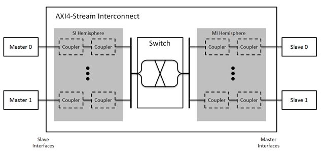
AXI4-Stream Interconnect
Note: AXI4-Stream Interconnect requires Vivado IP Integrator.
• Supports 1-16 slaves
AXI4-Stream Infrastructure IP Suite v2.2 www.xilinx.com Send Feedback
8
PG085 April 4, 2018Chapter 1: Overview
• Combines AXI4-Stream Switch with buffering modules, AXI4-Stream Data Width
Converter and AXI4-Stream Subset Converter to allow masters and slaves with varying
AXI4-Stream characteristics to exchange AXI4-Stream transfers.
System Requirements
For a list of System Requirements, see the Xilinx Design Tools: Release Notes Guide.
Licensing and Ordering Information
This Xilinx LogiCORE™ IP module is provided at no additional cost with the Xilinx Vivado ®
Design Suite under the terms of the Xilinx End User License. Information about this and
other Xilinx LogiCORE IP modules is available at the Xilinx Intellectual Property page. For
information about pricing and availability of other Xilinx LogiCORE IP modules and tools,
contact your local Xilinx sales representative.
AXI4-Stream Infrastructure IP Suite v2.2 www.xilinx.com Send Feedback
9
PG085 April 4, 2018Chapter 2
Product Specification
AXI4-Stream Infrastructure IP Suite Modules
AXI4-Stream Broadcaster
The AXI4-Stream Broadcaster provides a solution for replicating a single inbound
AXI4-Stream interface into multiple outbound AXI4-Stream interfaces. Support for up to 16
outbound AXI4-Stream interfaces is provided. Each outbound interface also supports an
optional remapping feature that allows you to select which TDATA (or TUSER) bits from the
inbound interface are present on the TDATA (or TUSER) port of each outbound interface. A
block diagram of the broadcaster is shown in Figure 2-1.
M
X-Ref Target - Figure 2-1
4$!4!453%2
2EMAPPER
4$!4!453%2
2EMAPPER
4$!4!453%2
2EMAPPER
8
Figure 2‐1: AXI4-Stream Broadcaster Block Diagram
AXI4-Stream Infrastructure IP Suite v2.2 www.xilinx.com Send Feedback
10
PG085 April 4, 2018Chapter 2: Product Specification
AXI4-Stream Clock Converter
Clock converters are necessary in the AXI4-Stream protocol for converting masters
operating at different clock rates to slaves. Typically, the AXI4-Stream Infrastructure IP
should be clocked at the same rate as the fastest slave and devices not running at that same
rate need to be converted. Synchronous clock converters are ideal because they have the
lowest latency and smaller area. However, they are only viable if both clocks are
phase-aligned, integer clock ratios, and the F MAX requirements are able to be met.
Asynchronous clock converters are a generic solution able to handle both synchronous/
asynchronous clocks with arbitrary phase alignment. The trade-off is that there is a
significant increase in area and latency associated with asynchronous clock converters. If
global clock enables are configured, additional logic is generated to handle clock enables
independently for each clock domain. There is a Clock converter module available in every
datapath and it is instantiated if either the clocks are specified as asynchronous or have
different synchronous clock ratios. The Clock converter module performs the following
functions:
• A clock-rate reduction module performs integer (N:1) division of the clock rate from its
input (SI) side to its output (MI) side.
• A clock-rate acceleration module performs integer (1:N) multiplication of clock rate
from its input (SI) to output (MI) side.
• Asynchronous clock rate conversion between the input and output uses an internal
FIFO Generator instantiated module.
• Clock enable crossing logic that handles different ACLKEN signals per clock domain.
Figure 2-2 shows the clock converter with support for independent ACLKEN signals on its
SI and MI.
AXI4-Stream Infrastructure IP Suite v2.2 www.xilinx.com Send Feedback
11
PG085 April 4, 2018Chapter 2: Product Specification
M
X-Ref Target - Figure 2-2
#LOCK #ONVERTER -ODULE
%NDPOINT %NDPOINT
#LOCK #ROSSING
-ASTER 3LAVE
,OGIC
-) 3) -) 3)
!#,+%. 3)?!#,+%. -)?!#,+%. !#,+%.
#LK ! #LK "
8
Figure 2‐2: Clock Converter Module Block Diagram
AXI4-Stream Combiner
The AXI4-Stream Combiner provides a solution for aggregating multiple narrow inbound
AXI4-Stream interfaces into a single wide outbound AXI4-Stream interface. Support for up
to 16 inbound AXI4-Stream interfaces is provided. A block diagram of the AXI4-Stream
Combiner is shown in Figure 2-3. A common use case of this solution is to merge three
separate red, green, blue video streams into a single RGB stream.
The combiner concatenates the incoming streams signals TDATA/TSTRB/TKEEP/TUSER to
create a single output stream that is the combination of the input streams. The TLAST/TID/
TDEST signals are taken from a single slave interface and the primary slave interface is
configurable.
IMPORTANT: All slave interfaces must assert the TVALID signal before the TVALID signal on the output
is asserted.
AXI4-Stream Infrastructure IP Suite v2.2 www.xilinx.com Send Feedback
12
PG085 April 4, 2018Chapter 2: Product Specification
M
X-Ref Target - Figure 2-3
AXIS?COMBINER
!8) 3TREAM;= 0AYLOAD;=
0AYLOAD;=
!8) 3TREAM;= !8)
3TREAM
!8) 3TREAM;=
0AYLOAD;=
8
Figure 2‐3: AXI4-Stream Combiner Block Diagram
AXI4-Stream Data FIFO
The FIFO module is capable of providing temporary storage (a buffer) of the AXI4-Stream
data. The FIFO Buffer module should be used in between two endpoints when:
• More buffering than a register slice is desired.
• Store and forward: to accumulate a certain number of bytes from the master before
forwarding them to the slave (packet mode).
The FIFO module can also implement asynchronous clock conversion so that when
asynchronous clock conversion and FIFOs are enabled on the same interface, redundant
FIFOs are not instantiated. The FIFO module uses the Xilinx LogiCORE™ IP FIFO Generator
module. This supports native AXI4-Stream with the following features:
• Variable FIFO depths
• FIFO data widths from 8 to 4096 bits
• Independent or common clock domains
• Symmetric aspect ratios
• Asynchronous active-Low reset
AXI4-Stream Infrastructure IP Suite v2.2 www.xilinx.com Send Feedback
13
PG085 April 4, 2018Chapter 2: Product Specification
• Selectable memory type. The memory type is inferred as distributed RAM for depths of
32 or less and block RAM for all others.
• Operates in First-Word Fall-Through (FWFT) mode
• Occupancy interface
• Both FIFO Generator rd_data_count and wr_data_count are passed as separate
outputs synchronized to the read side and write side clock domains.
AXI4-Stream Data Width Converter
Data width converters (upsizer/downsizer) are required when interfacing different data
width cores with each other. One data width conversion module is available to handle all
supported combinations of data widths.
The conversion follows the AMBA® AXI4-Stream Protocol Specification with regards to
ordering and expansion of TUSER bits. The width converter does not process any special
TUSER encoding formats; it only maps TUSER bits across the width conversion function
using the algorithm specified in the AXI4-Stream protocol specification. Depending on the
usage/meaning of TUSER to the endpoint IP, additional external logic might be required to
manipulate TUSER bits that have been transformed by the width converter.
IMPORTANT: The number of TUSER bits per TDATA bytes must remain constant between input and
output.
Up-conversion requires that each incoming beat that is composed of the new larger beat
consists of identical TID and TDEST bits and no intermediate TLAST assertions. Partial data
may be flushed when either the TLAST bit is received or TID/TDEST changes before
enough data is accumulated to send out a complete beat. Unassigned bytes are flushed out
as null bytes.
RECOMMENDED: Monitor the TKEEP signal output if TID/TDEST/TLAST signal is present.
Any non-integer multiple byte ratio conversion (N:M) is accomplished by calculating the
lowest common multiple (LCM) of N and M and then up-converting from N:LCM then
down-converting from LCM:M.
Up-conversion features:
• Range: Input 1-256 Bytes, Output 2-512 Bytes
• Supports full range of 1:N byte ratio conversions
• Minimum latency of 2 + N clock cycles in 1:N byte ratio up-conversion.
Down-conversion features:
• Range: Input 2-512 bytes, output 256-1 bytes
AXI4-Stream Infrastructure IP Suite v2.2 www.xilinx.com Send Feedback
14
PG085 April 4, 2018Chapter 2: Product Specification
• Supports full range of N:1 byte ratio conversions
• Minimum Latency: 2 clock cycles
X-Ref Target - Figure 2-4
$ATA #ONVERTER -ODULE
%NDPOINT BITS BITS %NDPOINT
-ASTER -) 3) -) 3) 3LAVE
8
Figure 2‐4: Data Width Converter (Down Conversion) Module Block Diagram
AXI4-Stream Register Slice
The register slice is a multipurpose pipeline register that is able to isolate timing paths
between master and slave. The register slice is designed to trade-off timing improvement
with area and latency necessary to form a protocol compliant pipeline stage. Implemented
as a two-deep FIFO buffer by default, the register slice supports throttling by the master
(channel source) and/or slave (channel destination) as well as back-to-back transfers
without incurring unnecessary idle cycles. The module can be independently instantiated at
all port boundaries. A configuration parameter allows for the trade off of performance vs.
area efficiency, including a mode that adds extra pipeline stages to optimally cross super
logic regions (SLR) boundaries in stacked silicon interconnect (SSI) devices.
AXI4-Stream Subset Converter
The AXI4-Stream Subset Converter provides a solution for connecting slightly incompatible
AXI4-Stream signal sets together. The IP has configurable AXI4-Stream signals for each
interface that allows one to convert one signal set to another in consistent manner.
All signals can be configured to be removed or added and additionally the TDATA, TUSER,
TSTRB, TKEEP, TID, TDEST, and TLAST signals can be remapped.
CAUTION! Due to the inherent data loss, care should be taken to fully understand the payload content
when converting to a signal set with fewer signals.
When signals are added, they are assigned default values as specified by the AMBA
specification. The TLAST signal can be added with a configurable assertion counter that
allows one to packetize their data. The REMAP functionality can be used to re-order TDATA
AXI4-Stream Infrastructure IP Suite v2.2 www.xilinx.com Send Feedback
15
PG085 April 4, 2018Chapter 2: Product Specification
bytes when working with core that have slightly different notations for data storage and
propagation.
AXI4-Stream Switch
The AXI4-Stream Switch provides configurable routing between masters and slaves. It
supports up to 16 masters and 16 slaves, two routing options, and multiple arbitration
options.
The two routing options available are TDEST routing and control register routing. The
TDEST based routing uses RTL parameters configured before synthesis to control the
routing. Each master interface is assigned a base/high TDEST pair that is used to generate
a decode table. Each slave interface decodes the incoming transfer based on the valid
TDEST value and routes a request to an arbiter of one of the master interfaces. When the
arbiter responds with a grant, then the slave interface proceeds with the transfer.
Arbitration can be performed at the transfer level or at the transaction level. (A transaction
is a series of two or more transfers.) Transaction level arbitration can be set to either
arbitrate at either fixed lengths or at TLAST boundaries. An optional timeout option is
available that terminates the transaction before the fixed length or TLAST is received if the
connection is idle for too long. This can help avoid deadlock in certain system topologies.
TDEST based routing requires that the signal has at least log2(Number of Slave Interfaces)
number of bits.
Control register routing introduces an AXI4-Lite interface to configure the routing table.
There is one register for each of the master interfaces to control each of the selectors. Once
the registers have been programmed, a commit register transfers the programmed values
from the register interface into the switch. During this period, the AXI4-Stream interfaces
are held in reset. This routing mode requires that there is precisely only one path between
master and slave. When attempting to map the same slave interface to multiple master
interfaces, only the lowest master interface is able to access the slave interface. Unused
master interfaces may be disabled and any unmapped slave interfaces are disabled.
Sparse connectivity between slave and master interfaces can be configured. This allows
resources to be conserved when they are not needed or to prevent invalid routes. For each
slave interface and master interface, a grid is created to allow you to deselect connectivity
during IP configuration. Invalid routes stall if using control register based routing and drop
transfers in the TDEST based routing. When transfers are dropped, the appropriate
decode_err signal is asserted.
Standards
The IP cores have bus interfaces that comply with the ARM® AMBA AXI4-Stream Protocol
Specification Version 1.0.
AXI4-Stream Infrastructure IP Suite v2.2 www.xilinx.com Send Feedback
16
PG085 April 4, 2018Chapter 2: Product Specification
Performance
The performance of an AXI4-Stream Infrastructure IP core is limited only by the FPGA logic
speed. Each core utilizes only block RAMs, LUTs, and registers and contains no I/O elements.
The values presented in this section should be used as an estimation guideline, actual
performance can vary.
Maximum Frequencies
Each core is designed to meet the maximum target frequency of 250 MHz on a Kintex ®-7
FPGA (xc7k325tffg900-1.) It can be expected that an -2 speed grade part can achieve 5%
higher maximum target frequency and that a -3 speed grade part can achieve 10% higher
maximum target frequency. For AXI4-Stream Switch configurations with more than
approximately four masters or slaves, the target maximum frequency can be reduced by
20-25%.
Latency
The latency in the IP cores can vary on an interface-to-interface basis, depending on how
the IP cores are configured. The latency is calculated in clocked cycles and is measured as
the time that it takes from the assertion of the slave interface TVALID signal to the first
assertion of the master interface TVALID signal. The latency for each of the individual
modules is listed in Table 2-1. To obtain the minimum latency for the system, add up the
values shown in the following tables for the modules in your system. The latency
specifications assume that the master interface TREADY signal input is always asserted. The
back-to-back delay is the number of clock cycles that back-to-back transfers can be
accepted by the module. This can be observed by counting how many cycles slave interface
TREADY is Low after a transfer is accepted on the interface.
Table 2‐1: Latency by Module Type
Latency Back-To-Back
Module Type Description
(clocks) Delay (clocks)
AXI4-Stream 0 0 The datapath of the broadcaster is combinatorial. It
Broadcaster exhibits no latency if all M_AXIS interfaces have
TREADY asserted.
AXI4-Stream Clock 1 0 The synchronous clock converter latency is reported
Converter as units of the slave interface clock.
(synchronous,
speed-up)
AXI4-Stream Infrastructure IP Suite v2.2 www.xilinx.com Send Feedback
17
PG085 April 4, 2018Chapter 2: Product Specification
Table 2‐1: Latency by Module Type (Cont’d)
Latency Back-To-Back
Module Type Description
(clocks) Delay (clocks)
AXI4-Stream Clock 1 [clock ratio]-1 The synchronous clock converter latency is reported
Converter as units of the slave interface clock. The back-to-back
(synchronous, delay varies based on the clock ratio.
speed-down) Example: If using a synchronous 150 MHz-to-50 MHz
3:1 clock converter (clock ratio of 3), the back-to-back
delay is 2 clock cycles.
AXI4-Stream Clock Not 0 The latency associated with an asynchronous clock
Converter Defined converter can vary greatly depending on the clocks. It
(asynchronous) can be expected to see latencies of 5 clock cycles or
more. See the FIFO Generator Product Guide v9.2
(PG057) [Ref 6] for more details.
AXI4-Stream 0 0 The datapath of the Combiner module is
Combiner combinatorial and thus has no latency if all ready/
valid inputs are asserted.
FIFO Generator 3 0 The FIFO when configured in normal mode outputs
AXI4-Stream (Data) data as soon as it is possible.
FIFO See the FIFO Generator Product Guide v9.2 (PG057)
[Ref 6] for more details.
FIFO Generator Until 0 When configured in packet mode, the FIFO outputs
AXI4-Stream Data TLAST is data only when a TLAST is received or the FIFO has
FIFO (packet mode) received filled.
or FIFO See the FIFO Generator Product Guide v9.2 (PG057)
is full. [Ref 6] for more details.
AXI4-Stream Data [data 0 The latency varies based on the data width ratio.
Width Converter width Example: If a 32 to 128-bit data converter is used (1:4
(upsizer) ratio] ratio), the latency of the module is 4 clock cycles.
AXI4-Stream Data 1 [data width The back-to-back delay varies based on the data
Width Converter ratio]-1 width ratio. Example: If a 32 to 16-bit data converter is
(downsizer) used (2:1 ratio), then the module can only accept
transfers every other cycle.
AXI4-Stream 1 0 Adding a register slice adds one cycle of latency. There
Register Slice is no back-to-back delay.
(default or
Fully-registered
mode)
AXI4-Stream 1 1 Adding a register slice adds one cycle of latency.
Register Slice Light-weight mode inserts one bubble cycle after
Lightweight mode each transfer.
AXI4-Stream 3 0 SLR Crossing mode incurs 3 latency cycles and adds
Register Slice SLR no back-to-back delay.
Crossing mode
AXI4-Stream 3 0 SLR TDM Crossing mode incurs 3 aclk latency cycles
Register Slice SLR and adds no back-to-back delay.
TDM Crossing
mode
AXI4-Stream Infrastructure IP Suite v2.2 www.xilinx.com Send Feedback
18
PG085 April 4, 2018Chapter 2: Product Specification
Table 2‐1: Latency by Module Type (Cont’d)
Latency Back-To-Back
Module Type Description
(clocks) Delay (clocks)
AXI4-Stream 0 0 Bypass mode directly connects the SI to the MI.
Register Slice
Bypass mode
AXI4-Stream 0-1 0 A register slice is inserted when there is a
Subset Converter m_axis_tready signal, but not a s_axis_tready signal to
avoid violation of the AXI4-Stream protocol. In this
configuration, the latency is 1 cycle, otherwise it is 0.
AXI4-Stream Switch 2 0-1 The output latency of the switch is 2 clock cycles.
There is 1 cycle of latency for the TDEST decode and 1
cycle of latency for the arbiter grant (if idle.) The
back-to-back delay for an already granted arbitration
is 0. Back-to back arbitration results in 1 cycle delays
between transactions.
Throughput
The throughput of a datapath through each AXI4-Stream Infrastructure IP is calculated as
TDATA width x clock frequency of each of the paths determined by the SI interface, and MI
interface. The minimum throughput of an individual path in a system for which the transfer
will traverse determines the overall throughput of the datapath.
Resource Utilization
The resource utilization of each AXI4-Stream Infrastructure IP is primarily a function of the
payload width of the stream. The payload width of the stream is calculated as the width of
the TDATA, TSTRB, TKEEP, TLAST, TID, TDEST and TUSER signals. For example, consider
the design that has the following signal widths listed in Table 2-2.
Table 2‐2: Signal Widths Used for Resource Utilization Estimation
AXI4-Stream Signal Width
TDATA 64
TSTRB 8
TKEEP 8
TLAST 1
TID 5
TDEST 6
TUSER 8
Total (Wp) 100
AXI4-Stream Infrastructure IP Suite v2.2 www.xilinx.com Send Feedback
19
PG085 April 4, 2018Chapter 2: Product Specification
The payload width W P is calculated as 64 + 8 + 8 + 1 + 5 + 6 + 8 = 100. The register slice
works as a double buffer and is able to hold two AXI4-Stream transfers at one time.
Therefore, a rough estimate of utilization can be achieved by multiplying the payload width
by two. This signal configuration from Table 2-2 is used in Table 2-3 as the basis for the
resource utilizations of the individual modules on a Kintex-7 FPGA (xc7k325tffg900-1) using
the Vivado synthesis tool. UltraScale™ results are expected to be similar to 7 series results.
Table 2‐3: Resource Utilization by Module Type
Block
Module Feature LUTs FFs
RAMs
2 Master Interfaces 5 2 0
AXI4-Stream Broadcaster 4 Master Interfaces 9 4 0
8 Master Interfaces 21 8 0
Asynchronous 104 287 0
AXI4-Stream Clock
Synchronous 2:1 109 211 0
Converter
Synchronous 1:2 107 209 0
2 Slave Interfaces 1 1 0
AXI4-Stream Combiner 4 Slave Interfaces 2 1 0
8 Slave Interfaces 4 1 0
Asynchronous, Depth 32 121 300 0
Asynchronous, Depth 512 109 260 2
Synchronous, Depth 32, Packet Mode 135 383 0
AXI4-Stream Data FIFO
Synchronous, Depth 32 101 247 0
Synchronous, Depth 512, Packet Mode 109 323 2
Synchronous, Depth 512 62 167 2
TDATA: 32 to 64 bits ( W P= 56 to W P=100) 35 164 0
TDATA: 32 to 128 bits (W P=56 to W P =188) 44 254 0
TDATA: 64 to 32 bits ( W P =100 to W P =56) 51 164 0
AXI4-Stream Data Width TDATA: 64 to 128 bits ( W P =100 to W P 35 296 0
Converter =188)
TDATA: 128 to 32 bits (W P =188 to W P =56) 129 257 0
TDATA: 128 to 64 bits ( W P =188 to W P 75 296 0
=100)
AXI4-Stream Register Slice Default 110 206 0
AXI4-Stream Subset No SI TREADY -> MI TREADY 105 198 0
Converter
AXI4-Stream Infrastructure IP Suite v2.2 www.xilinx.com Send Feedback
20
PG085 April 4, 2018Chapter 2: Product Specification
Table 2‐3: Resource Utilization by Module Type (Cont’d)
Module Feature LUTs FFs Block
RAMs
1 slave interface x 2 master interfaces 123 216 0
1 slave interface x 4 master interfaces 130 220 0
2 slave interface x 1 master interfaces 68 13 0
AXI4-Stream Switch
2 slave interface x 2 master interfaces 376 454 0
4 slave interface x 1 master interfaces 133 27 0
4 slave interface x 4 master interfaces 1028 978 0
Port Descriptions
Global Signals
These signals are always present when there is a common clock between all interfaces of the
IP core.
Table 2‐4: Global Signals
Signal Direction Description
aclk Input Global Clock Signal. Drives the clocks on the AXI4-Stream Switch and
is the primary clock to the system.
aresetn Input Global Reset Signal. This active-Low signal drives the reset pins on
the AXI4-Stream Switch and is the primary reset of the system.
aclken Input Global ACLK Enable signals. Drives the ACLKEN pins on the
AXI4-Stream Switch and is the primary ACLKEN of the system.
aclk2x Input This auxiliary clock input is only enabled on the AXI4-Stream Register
Slice when configured in SLR TDM Crossing mode, and must be
exactly twice the frequency of aclk and generated from the same
clock source with zero phase shift.
Slave Interface Signals
The following table lists the signals associated with each slave interface. If the number of
interfaces is configurable, then the signals in Table 2-5 are replicated for each port. The nn
denoted for the signals starts at 00 and increments by one up to 15 for each slave interface
instantiated. For IPs that contain only one slave interface the nn value is dropped. For
example, the Snn_AXIS_TVALID would be S_AXIS_TVALID. IP cores that do not support
multiple clocks do not have the Snn_AXIS_ACLK, Snn_AXIS_ARESETN, or the
Snn_AXIS_ACLKEN signals.
AXI4-Stream Infrastructure IP Suite v2.2 www.xilinx.com Send Feedback
21
PG085 April 4, 2018Chapter 2: Product Specification
Table 2‐5: Signals Associated with the Slave Interface
Signal Direction Description
Clock signal. All inputs/outputs of this bus
snn_axis_aclk Input interface are rising edge aligned with this
clock.
snn_axis_aresetn Input Active-Low synchronous reset signal
snn_axis_aclken Input Clock enable signal
TVALID indicates that the master is driving
a valid transfer.
snn_axis_tvalid (1) Input
A transfer takes place when both TVALID
and TREADY are asserted.
TREADY indicates that the slave can accept
snn_axis_tready(1) Output
a transfer in the current cycle.
TDATA is the primary payload that is used
snn_axis_tdata to provide the data that is passing across
Input
[(C_MNN_AXIS_TDATA_WIDTH-1):0](1) the interface. The width of the data payload
is an integer number of bytes.
TSTRB is the byte qualifier that indicates
snn_axis_tstrb whether the content of the associated byte
Input
[((C_MNN_AXIS_TDATA_WIDTH/8)-1):0] (1) of TDATA is processed as a data byte or a
position byte.
TKEEP is the byte qualifier that indicates
whether the content of the associated byte
of TDATA is processed as part of the data
snn_axis_tkeep
Input stream.
[((C_MNN_AXIS_TDATA_WIDTH/8)-1):0] (1)
Associated bytes that have the TKEEP byte
qualifier deasserted are null bytes and can
be removed from the data stream.
snn_axis_tlast (1) Input TLAST indicates the boundary of a packet.
snn_axis_tid TID is the data stream identifier that
Input
[C_NATIVE_TID_WIDTH-1:0](1) indicates different streams of data.
snn_axis_tdest TDEST provides routing information for the
Input
[(C_NATIVE_TDATA_WIDTH-1):0](1) data stream.
TUSER is user-defined sideband
snn_axis_tuser
Input information that can be transmitted
[(C_SNN_AXIS_TUSER_WIDTH-1):0] (1)
alongside the data stream.
AXI4-Stream Switch only signal.
Active-High signal to skip this bus on the
next arbitration cycle. While the signal is
s_req_suppress[C_NUM_SI_SLOTS-1:0] Input asserted, this bus does not receive the next
arbitration. If this bus already has
arbitration granted, it remains granted until
the arbitration cycle is completely normally.
AXI4-Stream Infrastructure IP Suite v2.2 www.xilinx.com Send Feedback
22
PG085 April 4, 2018Chapter 2: Product Specification
Table 2‐5: Signals Associated with the Slave Interface (Cont’d)
Signal Direction Description
AXI4-Stream Switch only signal. One-hot
output indicates that a incoming transfer
has a TDEST value that not map to a valid
s_decode_err[C_NUM_SI_SLOTS-1:0] Output
Master Interface. Invalid TDEST transfers
are dropped. Only valid if the TDEST signal
is present and used for routing.
AXI4-Stream Subset Converter only signal.
This signal is only present if the Slave
Interface TREADY signal is not enabled and
transfer_dropped Output the Master interface TREADY signal is
enabled. This signal indicates if there is an
AXI-S transfer that has been dropped due
to a de-asserted MI TREADY.
AXI4-Stream Subset Converter only signal.
This signal is only present if the Slave
Interface TKEEP is enabled and the Master
sparse_tkeep_removed Output Interface TKEEP is not enabled. This signal
signals if there is a Slave Interface TKEEP
that has been removed and null data bytes
were present.
AXI4-Stream Combiner only. This output is
s_cmd_err[(C_NUM_SI_SLOTS*3)-1:0] Output
not defined and may change in the future.
AXI4-Stream Data FIFO only. Indicates the
count inside the DATA FIFO. This signal can
axis_data_count[31:0] Output
be used when using common clocks
between interfaces.
AXI4-Stream Data FIFO Only. Indicates the
write count inside the DATA
axis_wr_data_count[31:0] Output FIFO. This signal can be used when using
asynchronous clocking and can be sampled
on the posedge of the s_axis_aclk.
1. This signal description is taken from the ARM AMBA Protocol Specification.
Master Interface Signals
Table 2-6 lists the signals associated with each master interface. If the number of interfaces
is configurable, the signals are then replicated for each port. The nn denoted for the signals
starts at 00 and increments by one up to 15 for each master interface instantiated. For IPs
that contain only one master interface the nn value is dropped. For example, the
Mnn_AXIS_TVALID would be M_AXIS_TVALID. IPs that do not support multiple clocks do
not have the Mnn_AXIS_ACLK, Mnn_AXIS_ARESETN, or the Mnn_AXIS_ACLKEN signals.
AXI4-Stream Infrastructure IP Suite v2.2 www.xilinx.com Send Feedback
23
PG085 April 4, 2018Chapter 2: Product Specification
Table 2‐6: Signals Associated with the Master Interface
Signal Direction Description
Clock signal. All inputs/outputs of this
mnn_axis_aclk Input bus interface are rising edge aligned
with this clock.
mnn_axis_aresetn Input Active-Low synchronous reset signal
mnn_axis_aclken Input Clock enable signal
TVALID indicates that the master is
driving a valid transfer.
mnn_axis_tvalid (1) Output
A transfer takes place when both TVALID
and TREADY are asserted.
TREADY indicates that the slave can
mnn_axis_tready(1) Input
accept a transfer in the current cycle.
TDATA is the primary payload that is
used to provide the data that is passing
mnn_axis_tdata
Output across the interface. The width of the
[(c_mnn_axis_tdata_width-1):0] (1)
data payload is an integer number of
bytes.
TSTRB is the byte qualifier that indicates
mnn_axis_tstrb whether the content of the associated
Output
[((c_mnn_axis_tdata_width/8)-1):0](1) byte of TDATA is processed as a data byte
or a position byte.
TKEEP is the byte qualifier that indicates
whether the content of the associated
byte of TDATA is processed as part of the
mnn_axis_tkeep data stream.
Output
[((c_mnn_axis_tdata_width/8)-1):0](1) Associated bytes that have the TKEEP
byte qualifier deasserted are null bytes
and can be removed from the data
stream.
TLAST indicates the boundary of a
mnn_axis_tlast (1) Output
packet.
mnn_axis_tid TID is the data stream identifier that
Output
[c_native_tid_width-1:0](1) indicates different streams of data.
mnn_axis_tdest TDEST provides routing information for
Output
[(c_native_tdata_width-1):0](1) the data stream.
TUSER is user-defined sideband
mnn_axis_tuser
Output information that can be transmitted
[(c_snn_axis_tuser_width-1):0](1) alongside the data stream.
AXI4-Stream Data FIFO Only. Indicates
the read count inside the DATA
axis_rd_data_count[31:0] Output FIFO. This signal can be used when using
asynchronous clocking and can be
sampled on the posedge of the
m_axis_aclk.
1. This signal description is taken from the ARM AMBA Protocol Specification.
AXI4-Stream Infrastructure IP Suite v2.2 www.xilinx.com Send Feedback
24
PG085 April 4, 2018Chapter 2: Product Specification
AXI4-Lite Interface Signals
Table 2-7 lists the signals associated with the optional AXI4-Lite control register interface.
This interface is optional and only present on a subset of IPs.
Table 2‐7: Optional AXI4-Lite Interface Signals
Signal(1) Direction Description
s_axi_ctrl_aclk Input Clock signal. All inputs/outputs of this bus interface are rising edge
aligned with this clock.
s_axi_ctrl_aresetn Input Active-Low synchronous reset signal
s_axi_ctrl_awalid Input Write address valid. This signal indicates that the channel is signaling
valid write address.
s_axi_ctrl_awready Output Write address ready. This signal indicates that the slave is ready to
accept an address.
s_axi_ctrl_awaddr Input Write address. The write address gives the address of the transaction.
s_axi_ctrl_wvalid Input Write valid. This signal indicates that valid write data are available.
s_axi_ctrl_wready Output Write ready. This signal indicates that the slave can accept the write
data.
s_axi_ctrl_wdata Input Write data.
s_axi_ctrl_bvalid Output Write response valid. This signal indicates that the channel is signaling
a valid write response.
s_axi_ctrl_bready Input Write response ready. This signal indicates that the master can accept
a write response.
s_axi_ctrl_bresp Output Write response. This signal indicate the status of the write transaction.
s_axi_ctrl_arvalid Input Read address valid. This signal indicates that the channel is signaling
valid read address.
s_axi_ctrl_arready Output Read address ready. This signal indicates that the slave is ready to
accept an address.
s_axi_ctrl_araddr Input Read address. The read address gives the address of the transaction.
s_axi_ctrl_rvalid Output Read valid. This signal indicates that the channel is signaling the
required read data.
s_axi_ctrl_rready Input Read ready. This signal indicates that the master can accept the read
data and response information.
s_axi_ctrl_rdata Output Read data.
s_axi_ctrl_rresp Output Read response. This signal indicate the status of the read transfer.
1. This signal description is taken from the ARM AMBA Protocol Specification.
AXI4-Stream Infrastructure IP Suite v2.2 www.xilinx.com Send Feedback
25
PG085 April 4, 2018Chapter 2: Product Specification
Register Space
AXI4-Stream Switch
The AXI4-Stream switch has a Control Register interface option that can be enabled when
the Use control register routing option is set to Yes. Table 2-8 describes the register map.
Table 2‐8: Register Map
Access Double
Address Offset Name Type Buffered Default Value Description
0x0000 Control R/W Yes 0x0 General control
0x0004-0x003C Reserved 0x0
0x0040-0x007F MI_MUX[0-1 R/W Yes 0x80000000 MI selector value
5]
Control Register
This register is responsible for committing the MI selector values from the control register
block to the AXI4-Stream Switch block. This register has a single bit that commits the
change. The commit causes the AXI4-Stream switch to go into a soft reset for approximately
16 cycles. This register is self-clearing when the commit/reset is complete.
Table 2‐9: Control Register
Name Bits Description
Reserved 0 Reserved
REG_UPDATE 1 Register Update. MUX registers are double buffered. Writing '1'
updates the registers and issues a soft reset to the core (for
approximately 16 cycles.)
Reserved 31:2 Reserved
MI_MUX[0-15] Register
There is one MI_MUX register for each number of master interfaces ports in the design. Each
MIx_MUX value controls slave interface selection. For example, MI4_MUX value of 0x1
would route slave interface 1 to master interface 4. The MIx_DISABLE value can be set to
disable the master interface. Each slave interface can only be selected once. If more than 1
MIx_MUX value is set to the same slave interface, then the lower master interface wins
control and the higher master interface(s) is disabled. MI0_MUX register is at address offset
0x40, MI1_MUX_register is at address offset 0x44, …, and MI15_MUX register is at address
offset 0x7C.
AXI4-Stream Infrastructure IP Suite v2.2 www.xilinx.com Send Feedback
26
PG085 April 4, 2018Chapter 2: Product Specification
Table 2‐10: MI Mux Registers
Name Bits Description
MIx_MUX 3:0 MIx Mux Value
MIx_DISABLE 31 Set to 1 to explicitly disable
Note: x is 0-15
Usage
To configure a 4x4 switch where MI0 is sourced from SI1, MI1 is unused, MI2 is sourced from
SI3 and MI3 is sourced from SI0, use the following code example:
# Setup registers
Write address offset 0x40, Data 0x1
Write address offset 0x44, Data 0x8000_0000
Write address offset 0x48, Data 0x3
Write address offset 0x4C, Data 0x0
# Commit registers
Write address offset 0x0, data 0x2
AXI4-Stream Infrastructure IP Suite v2.2 www.xilinx.com Send Feedback
27
PG085 April 4, 2018Chapter 3
Designing with the Core
This chapter includes guidelines and additional information to make designing with the
core easier.
General Design Guidelines
When designing systems using AXI4-Stream Infrastructure IP Suite, the first step is to
establish the topology of the system. This requires an understanding of the main interface
characteristics of each AXI4-Stream master and slave that needs to be able to communicate
together. AXI4-Stream masters and slaves then need to be grouped by desired connectivity
into a system with one or more AXI4-Stream Infrastructure IP blocks tying them together so
they can exchange data.
In general, try to establish the system partitioning/topology to use multiple smaller/simpler
interconnects than a single large interconnect, especially in systems with a large number of
devices. For example, combinations of N master x 1 slaves interconnects and 1 master x N
slave interconnects are generally preferable to MxN interconnects in terms of area, latency,
and throughput. MxN interconnect when required for performance or connectivity
requirements should try to limit the number of endpoints or specify sparse connectivity to
reduce resource utilization.
The Xilinx Vivado AXI Reference Guide (UG1037) [Ref 3] provides information about
AXI4-Stream protocol usage guidelines and conventions; much of the AXI system
optimizations information described for AXI Interconnect is applicable to AXI4-Stream
Infrastructure IP Suite. The Xilinx AXI Reference Guide should be reviewed and consulted
before designing or structuring systems around the AXI4-Stream Infrastructure IP.
After the number and topology of AXI4-Stream Infrastructure IP systems have been
determined, the next step is to tailor each AXI4-Stream Infrastructure IP system to have the
correct set of optional interface signals and set signals’ widths as needed. This sets up the
interface signal set for the AXI4-Stream Infrastructure IP to ensure that data can be
exchanged and routed as needed across the system.
Finally, the AXI4-Stream Infrastructure IP system should be optimized and fine-tuned to fit
its application. This includes tuning FIFOs, width converters, clock converters, arbiters, and
register slices (pipeline stages) as needed to balance area, timing, performance, and
ease-of-use.
AXI4-Stream Infrastructure IP Suite v2.2 www.xilinx.com Send Feedback
28
PG085 April 4, 2018Chapter 3: Designing with the Core
Clocking
Each AXI4-Stream Infrastructure IP module has a single clock input that must be driven with
the exception of AXI4-Stream Clock Converter and AXI4-Stream Data FIFO. These modules
allow for different clocks and must have both S_AXIS_ACLK and M_AXIS_ACLK
connected.
The AXI4-Stream Clock Converter and Data FIFO allows systems with different clock
domains to be designed. AXI4-Stream Clock Converter synchronous mode can be used
when the endpoint IP has a phase-aligned, integer multiple clock ratio to the core switch's
clock. This is often the case when the same MMCM or PLL is driving synchronous integer
ratio clocks because the MMCM/PLL can also ensure phase alignment across their clock
outputs. The AXI4-Stream Clock Converter and AXI4-Stream Data FIFO asynchronous
clocking mode allows the attached endpoint IP to run at a completely unrelated clock
frequency or phase to the core switch clock. Embedded asynchronous FIFOs from FIFO
Generator are instantiated inside the modules to handle data transfers across asynchronous
clock domains in a robust manner.
An optional feature for clock enables (ACLKEN ports) allows an extra level of control for
essentially gating clocks. The clock enable signals can be used to control which clock edges
are seen as real transfer cycles. Clock enables can be used for purposes like preserving
global clock buffers, debug by stepping the clock enable to step through operational states
in the system, and dynamic power savings. Clock enables can be controlled independently
on each interface port and for the core switch.
The optional AXI4-Lite control register interface operates asynchronously from the
AXI4-Stream clocks.
AXI4-Stream Infrastructure IP Suite v2.2 www.xilinx.com Send Feedback
29
PG085 April 4, 2018Chapter 3: Designing with the Core
Resets
The AXI4-Stream Infrastructure IP Suite provides active-Low reset inputs for every clock
input on the IP. Each reset input must be synchronized to the associated ACLK input of the
interface. To ensure data is not lost during reset de-assertion across multiple interfaces of
the AXI4-Stream Infrastructure IP systems (operating in potentially different clock domains),
the AXI4-Stream Infrastructure IP will de-assert all TREADY and TVALID outputs until the
clock cycle after their source logic has internally exited reset. Any endpoint IP driving
TREADY or TVALID inputs to the AXI4-Stream Infrastructure IP should also de-assert these
signals until the clock cycle after they have exited reset internally.
These guidelines ensure that endpoint IPs can internally come out of reset at different times
(due to internal reset pipelining) and no data will be exchanged until both are internally out
of reset.
RECOMMENDED: Any endpoint should de-assert TREADY and TVALID within 8 clock cycles of reset
assertion. ARESETn should also be asserted for at least 16 cycles of the slowest system clock to ensure
that all AXI4-Stream interfaces in the system enter reset and have time to de-assert their TREADY/
TVALID outputs before coming back out of reset.
AXI4-Stream Infrastructure IP Suite v2.2 www.xilinx.com Send Feedback
30
PG085 April 4, 2018Chapter 4
Design Flow Steps
This chapter describes customizing and generating the core, constraining the core, and the
simulation, synthesis and implementation steps that are specific to this IP core. More
detailed information about the standard Vivado® design flows in the IP Integrator can be
found in the following Vivado Design Suite user guides:
• Vivado Design Suite User Guide: Designing IP Subsystems using IP Integrator (UG994)
[Ref 10]
• Vivado Design Suite User Guide: Designing with IP (UG896) [Ref 5]
• Vivado Design Suite User Guide: Getting Started (UG910) [Ref 8]
• Vivado Design Suite User Guide: Logic Simulation (UG900) [Ref 9]
Customizing and Generating the Core
This section includes information about using Xilinx tools to customize and generate the
core in the Vivado® Design Suite.
If you are customizing and generating the core in the Vivado IP Integrator, see the Vivado
Design Suite User Guide: Designing IP Subsystems using IP Integrator (UG994) [Ref 10] for
detailed information. IP Integrator might auto-compute certain configuration values when
validating or generating the design. To check whether the values do change, see the
description of the parameter in this chapter. To view the parameter value, run the
validate_bd_design command in the Tcl console.
Vivado Integrated Design Environment
You can customize the IP for use in your design by specifying values for the various
parameters associated with the IP core using the following steps:
1. Select the IP from the IP catalog.
2. Double-click on the selected IP or select the Customize IP command from the toolbar or
popup menu.
AXI4-Stream Infrastructure IP Suite v2.2 www.xilinx.com Send Feedback
31
PG085 April 4, 2018Chapter 4: Design Flow Steps
For details, see the sections, “Working with IP” and “Customizing IP for the Design” in the
Vivado Design Suite User Guide: Designing with IP (UG896) [Ref 5] and the “Working with the
Vivado IDE” section in the Vivado Design Suite User Guide: Getting Started (UG810) [Ref 8].
If you are customizing and generating the core in the Vivado IP Integrator, see the Vivado
Design Suite User Guide: Designing IP Subsystems Using IP Integrator (UG994) [Ref 10] for
detailed information. IP Integrator might auto-compute certain configuration values when
validating or generating the design. To check whether the values do change, see the
description of the parameter in this chapter. To view the parameter value you can run the
validate_bd_design command in the Tcl console.
Note: Figures in this chapter are illustrations of the Vivado IDE. This layout might vary from the
current version.
Creating a Project
First, create a new project using the Vivado Design Suite. For detailed information on
starting and using the Vivado Design Suite, see the Vivado documentation.
Perform the following steps:
1. Start the Vivado Design Suite.
2. Choose File > New Project from the menu.
3. Using the Create New Vivado Project wizard. Click Next.
4. Select a Project Name:
a. Modify the project name, if desired.
b. Specify the Project location using the text box or the directory navigator.
c. Click Next.
5. Select a Project Type:
a. Choose RTL Project.
b. Ensure the "Do not specify sources at this time" checkbox is checked.
c. Click Next.
6. Select the Default Part.
a. Select the target family, device, package, and speed grade.
Example: Kintex-7, xc7k325t-ffg900-1
Note: If an unsupported family is selected, the IP core does not appear in the IP catalog.
b. Click Next.
AXI4-Stream Infrastructure IP Suite v2.2 www.xilinx.com Send Feedback
32
PG085 April 4, 2018Chapter 4: Design Flow Steps
7. Review Project Summary.
a. If the summary does not look correct, click the Back button and resolve the issue.
b. Click Finish to create the project.
After creating the project, the IP cores are available for selection in the IP catalog, located
at AXI Infrastructure Taxonomy.
Customizing and Generating the Core
Locate the IP core in the Vivado Design Suite and click it once to select it. Details regarding
the solution are displayed in the Details window. To configure the IP, double-click the IP
name in the IP catalog.
This launches the customization dialog box. Each dialog box is described in detail in their
respective sections.
AXI4-Stream Broadcaster
The AXI4-Stream Broadcaster GUI is shown in Figure 4-1.
M
X-Ref Target - Figure 4-1
Figure 4‐1: AXI4-Stream Broadcaster Customization Dialog Box
AXI4-Stream Infrastructure IP Suite v2.2 www.xilinx.com Send Feedback
33
PG085 April 4, 2018You can also read


