1080p60 Camera Image Processing Reference Design
←
→
Page content transcription
If your browser does not render page correctly, please read the page content below
Application Note: Zynq-7000 All Programmable SoC Video and Imaging Kit

                                                             1080p60 Camera Image Processing
                                                             Reference Design
                                                             Authors: Mario Bergeron (Avnet, Inc.), Steve Elzinga, Gabor Szedo, Greg Jewett,
XAPP794 (v1.3) December 20, 2013                             and Tom Hill (Xilinx, Inc.)

Summary                                   The Xilinx Zynq®-7000 All Programmable (AP) SoC Video and Imaging Kit (ZVIK) builds on the
                                          Zynq-7000 AP SoC ZC702 evaluation kit (ZC702) [Ref 43] by including additional hardware,
                                          software, and IP components for the development of custom video applications. The included
                                          video reference designs, WUXGA color image sensor, and video I/O FPGA mezzanine card
                                          (FMC) with HDMI™ input and output allow for immediate development of video system
                                          software, firmware, and hardware designs.
                                          This application note describes how to set up and run the 1080p60 camera image processing
                                          reference design (camera design) using the ZVIK. Instructions are also included on how to
                                          build the hardware and software components as well as how to create the SD card boot image.
                                          The intended audience for this document includes video applications embedded system
                                          developers, hardware developers, and system architects. To learn more about the Zynq-7000
                                          AP SoC, the ZVIK, or for further development using the embedded design kit, consult the
                                          References section. The Appendix provides a list of acronyms used in this application note.

Introduction                              This application note describes the 1080p60 camera image processing reference design that
                                          showcases various features of the ZVIK, provides a working camera image processing
                                          example design, and introduces several Xilinx video IP cores.
                                          Video input is generated by the VITA-2000 image sensor from ON Semiconductor, which is
                                          configured for 1080p60 resolution. The raw Bayer sub-sampled image is converted to an RGB
                                          image by an image processing pipeline implemented using LogiCORE™ IP video cores that
                                          remove defective pixels, de-mosaic, and color-correct the image. A video frame buffer is
                                          implemented in the processing system (PS) DDR3 memory, making images accessible to the
                                          ARM® processor cores via the AXI Video Direct Memory Access (VDMA). The video frame
                                          buffer is not required for the operation of the image processing pipeline, but is included in the
                                          design to enable the capture of input video images for analysis. Figure 1 shows a block diagram
                                          of the design.

© Copyright 2013 Xilinx, Inc. Xilinx, the Xilinx logo, Artix, ISE, Kintex, Spartan, Virtex, Vivado, Zynq, and other designated brands included herein are trademarks of Xilinx in the
United States and other countries. ARM, AMBA, and CoreSight are trademarks of ARM in the EU and other countries. HDMI and High-Definition Multimedia Interface are
trademarks of HDMI Licensing LLC. MATLAB is a registered trademark of The MathWorks, Inc. All other trademarks are the property of their respective owners.

XAPP794 (v1.3) December 20, 2013                                                www.xilinx.com                                                                                     1
Introduction

X-Ref Target - Figure 1

                                                                              DDR3

                                          Processing
                                          System                     DDR Memory Controller
                            Firmware
                           on SD Card                                                                             S_AXI4_HPx
                                                                                                                  M_AXI4_GP

                                                                               AMBA® Switches                     AXI4 Stream

                                              Hardened
                                              Peripherals                       APU
                           PC running        (USB, GigE,                     Dual Core
                          Web-based GUI       CAN, SPI,                   Cortex-A9 + OCM
                                              UART, 12C
                                                GPIO)

                                                                 AMBA Switches

                                             Camera            Image                  AXI
                                              Input          Processing              VDMA
                                                              Pipeline                               HDMI
                                                                                                     Output
                            VITA-2000
                             Camera                                                          Programmable Logic          HDMI Monitor
                                                                                                                           X794_01_102512

                                                Figure 1:   1080p60 Camera Design Block Diagram

                                          A web-based graphical user interface (GUI) allows configuring each of the Xilinx video IP cores
                                          in the image processing pipeline, displaying information about the incoming image such as
                                          histograms of the data, and enables processor-based operations on the data such as automatic
                                          white balance and automatic exposure.
                                          The hardware evaluation cores contained in the design time out after approximately four hours,
                                          resulting in a blank screen. At this point, the board must be power-cycled to reload the design.

XAPP794 (v1.3) December 20, 2013                                     www.xilinx.com                                                         2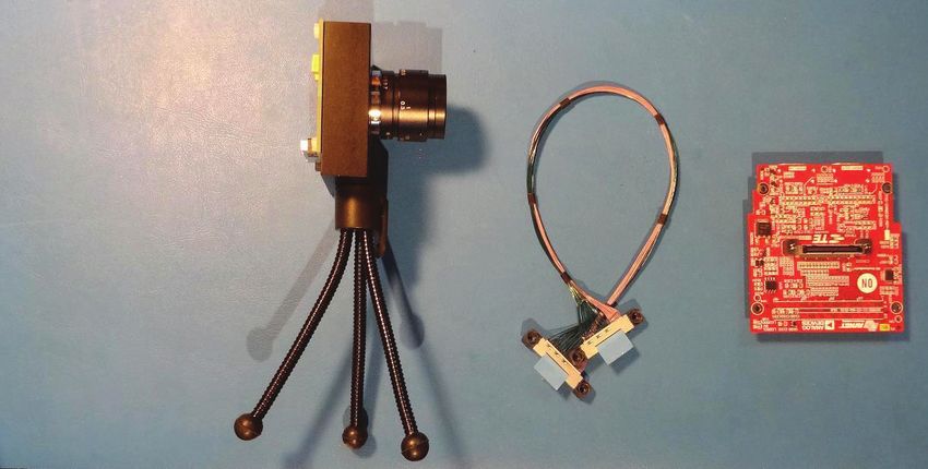
Introduction

                           Host PC System Requirements
                           The host PC requirements to operate the camera design and its applications are:
                           •   32-bit/64-bit host PC with Ethernet port running Windows XP or Windows 7 Professional
                               32-bit/64-bit, or Ubuntu 10 or later 32-bit/64-bit Linux distribution.
                           •   UART connected terminal (for example, Tera Term 4.69 or HyperTerminal).
                           •   Zip/Unzip software (for example, 7-Zip).
                           •   Web browser such as Internet Explorer (to operate the web-based GUI).
                           •   USB-UART driver from Silicon Labs [Ref 39] (might already be installed). For information
                               about installing the USB-UART driver, see Zynq-7000 All Programmable SoC: ZC702
                               Evaluation Kit and Video and Imaging Kit Getting Started Guide [Ref 1].
                           To build the hardware and software components, the Vivado® 2013.2 design tools are also
                           required.

                           Target Hardware Requirements
                           The target hardware requirements for running the camera design and its applications are:
                           •   Zynq-7000 All Programmable SoC Video and Imaging Kit, including:
                               •   Xilinx XC7Z020 CLG484-1 SoC-based ZC702 evaluation board.
                               •   Avnet FMC-IMAGEON FMC module.
                               •   VITA-2000 camera module (including optics, tripod, and cable).
                               •   HDMI cable.
                               •   SD-MMC flash card.
                               •   12V power supply.
                           •   HDMI monitor supporting 1080p60 resolution. A DVI monitor can also be used, but an
                               HDMI female to DVI-D male connector adapter must be obtained (not provided with the
                               kit). The connector adapter is available at most electronic retailers or through online
                               sources.
                           •   SD-MMC flash card writer.
                           For more information on the Zynq-7000 AP SoC Video and Imaging Kit, see:
                               www.xilinx.com/zvik
                           For more information on the Zynq-7000 AP SoC ZC702 evaluation board (including hardware
                           user manual, schematics, and BOM), see:
                               www.xilinx.com/zc702
                           For more information on the Avnet FMC-IMAGEON FMC Module with ON Semiconductor
                           image sensor, see:
                               www.em.avnet.com/fmc-imageon-v2000c

XAPP794 (v1.3) December 20, 2013                     www.xilinx.com                                                       3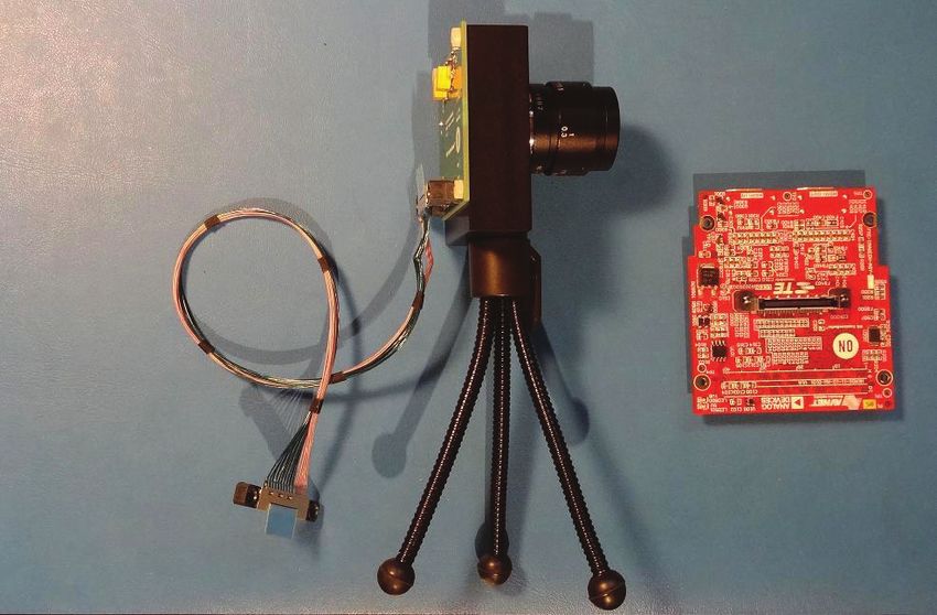
Running the Demonstration

Running the                This section describes how to run the 1080p60 camera image processing reference design on
Demonstration              the ZVIK.

                           Reference Design File
                           The reference design files for this application note can be downloaded from:
                           https://secure.xilinx.com/webreg/clickthrough.do?cid=199792
                           Table 1 shows the reference design matrix.

                           Table 1: Reference Design Matrix
                                                Parameter                                           Description
                            General
                            Developer name                                       Xilinx
                            Target devices                                       Zynq-7000 AP SoC
                            Source code provided                                 Yes
                            Source code format                                   VHDL (some sources encrypted)
                            IP used                                              Video IP Cores
                            Simulation
                            Functional simulation performed                      N/A
                            Timing simulation performed                          N/A
                            Test bench used for functional and timing            N/A
                            simulations
                            Test bench format                                    N/A
                            Simulator software/version used                      N/A
                            SPICE/IBIS simulations                               N/A
                            Implementation
                            Synthesis software tools/version used                Vivado 2013.2 design tools
                            Implementation software tools/version used           Vivado 2013.2 design tools
                            Static timing analysis performed                     Yes (pass timing in PAR/TRACE)
                            Hardware Verification
                            Hardware verified                                    Yes
                            Hardware platform used for verification              Zynq-7000 Video and Imaging Kit

                           Installing Design Files
                           Download the xapp794.zip files to the C: drive of the host PC:
                               C:\zc702-zvik-camera
                           Note: The Windows operating system has a 260 character limitation on the maximum length for a path.
                           Make sure that the installation path is short to prevent path length related errors. If another location is
                           chosen, there should be no spaces in the folder names.

XAPP794 (v1.3) December 20, 2013                        www.xilinx.com                                                               4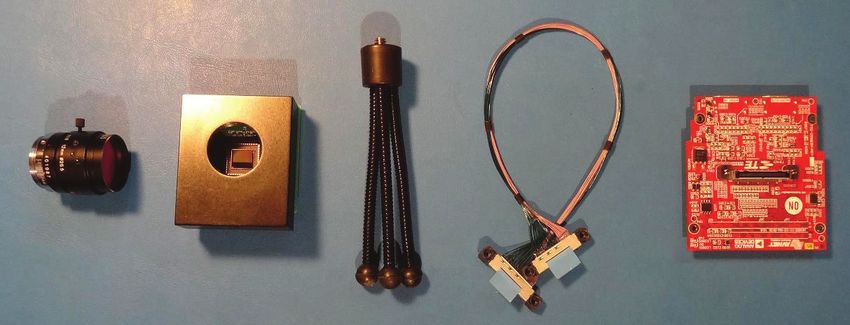
Running the Demonstration

                           Preparing the SD Card
                           Pre-built binaries for the camera design are provided in this directory:
                                               ..\zc702-zvik-camera\binaries\sd_content
                           Create a backup copy of the files on the SD card provided with the kit to enable them to be
                           restored if desired. These files are also available on the ZVIK product page. Copy the contents
                           of the sd_content directory to the root directory of the SD card.
                           By default, the design configures the ZVIK for IP address 192.168.1.10. This requires
                           configuring the host computer to a compatible IP address, such as 192.168.1.20. If this is not
                           possible, the IP address of the ZVIK in the configuration script should be changed:
                                               ..\zc702-zvik-camera\binaries\sd_content\config_my_ip.sh
                           On a Windows host, use a text editor that does not alter the end of line characters, such as
                           Notepad.
                           X-Ref Target - Figure 2

                                                                                                               X794_02_111512

                                                              Figure 2:   Modifying the ZVIK IP Address

                           With a subnet mask of 255.255.255.0, the first three number groups of the IP address must be
                           identical in both the host computer IP address and the ZVIK IP address. For example, if the
                           ZVIK is configured with the IP address 192.168.1.10 (and subnet mask 255.255.255.0), the
                           host must be configured with an IP address containing identical numbers in the first three
                           positions and a differing number in the fourth group, such as 192.168.1.20.

                           Configuring the Host IP Address
                           Configure the IP address of the host computer to one that is compatible with the ZVIK IP
                           address discussed in Preparing the SD Card. Record the host PC's original network settings so
                           they can be restored after running the demonstration. Configure the computer’s IP address to
                           192.168.1.20 (or similar). The subnet mask can be 255.255.255.0. The screen captures and
                           icon names shown in this section might be slightly different depending on the computer’s
                           operating system version.
                           For Windows 7:
                           1. Click the Start button and select Control Panel.
                           2. Select Network and Sharing Center.
                           3. Select Change Adapter Settings from the options on the left panel.
                           4. Right-click the adapter corresponding to the wired Ethernet port identified as a local area
                              connection and select Properties.
                           5. Accept the User Account Control dialog box by selecting Yes.
                           6. Click the Internet Protocol Version 4 (TCP/IPv4) entry and select Properties.
                           7. On the General tab, select Use the following IP address radio button.
                           8. In the IP address: field, enter 192.168.1.20 or a value that is compatible with the ZVIK IP
                              address configured in the previous section.

XAPP794 (v1.3) December 20, 2013                              www.xilinx.com                                                    5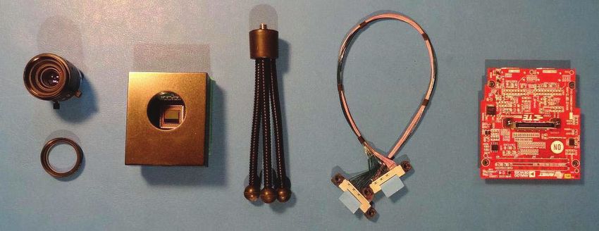
Running the Demonstration

                           9. Click the Subnet mask: field and ensure that it is populated with 255.255.255.0. The dialog
                              box should appear similar to Figure 3.
                           X-Ref Target - Figure 3

                                                                                                    X794_03_102512

                                                     Figure 3:   Host Computer IP Address Configuration Dialog Box

                           10. Select OK to close the Internet Protocol Version 4 (TCP/IPv4) dialog box. Select OK to
                               close the Local Area Connection Properties dialog box.

                           Assembling the Camera
                           If the camera assembly has been completed, go to Setting Up the Hardware.
                           The ZVIK package contains these components, which must be assembled:
                           1. IR cut filter
                           2. Lens (2/3”, 8 mm)
                           3. VITA-2000-C image sensor module (with C-mount lens holder)
                           4. Tripod
                           5. LCEDI cable
                           6. FMC-IMAGEON FMC module

XAPP794 (v1.3) December 20, 2013                                  www.xilinx.com                                        6
Running the Demonstration

                                  To assemble the camera:
                                  1. Remove both protective caps from the lens (2) (Figure 4).
X-Ref Target - Figure 4

                                                         4                        5

                          2
                                                                                                          6
                                  3

                              1

                                                                                                                        X794_04_102612

                                          Figure 4:   VITA-2000 Camera Assembly Step 1

                                  2. Attach the IR cut filter (1) to the lens (2) (Figure 5). The filter screws onto the front of the
                                     lens.
X-Ref Target - Figure 5

                                                             4

                                                                                  5
                                  3
                                                                                                          6

                                                                                                                        X794_05_102612

                                          Figure 5:   VITA-2000 Camera Assembly Step 2

XAPP794 (v1.3) December 20, 2013                                 www.xilinx.com                                                          7
Running the Demonstration

                           3. Screw the IR cut filter and lens assembly onto the VITA-2000 image sensor module (3)
                              (Figure 6). The image sensor module has a lens holder with an opening for standard
                              C-mount lenses.
X-Ref Target - Figure 6

                                                   4                    5

                                                                                              6

                                                                                                         X794_06_102612

                                   Figure 6:   VITA-2000 Camera Assembly Step 3

                           4. Attach the tripod (4) to the bottom of the VITA-2000 image sensor module (Figure 7). The
                              image sensor module lens holder has a hole that accepts standard tripods having a 1/4
                              inch screw with 20 threads per inch.
X-Ref Target - Figure 7

                                                                        5

                                                                                          6

                                                                                                      X794_07_102612

                                   Figure 7:   VITA-2000 Camera Assembly Step 4

XAPP794 (v1.3) December 20, 2013                       www.xilinx.com                                                     8
Running the Demonstration

                           5. Attach the LCEDI cable (5) to the back of the VITA-2000 image sensor module (Figure 8).
                              Both ends of the LCEDI are identical. Either end can be connected to the image sensor
                              module.
                           X-Ref Target - Figure 8

                                                                                                      6

                                                                                                            X794_08_102612

                                                               Figure 8: VITA-2000 Camera Assembly Step 5

                           6. Attach the other end of the LCEDI cable to the FMC-IMAGEON FMC module (6) (Figure 9).
                           X-Ref Target - Figure 9

                                                                                                            X794_09_102612

                                                               Figure 9: VITA-2000 Camera Assembly Step 6

                                               The VITA-2000 color camera assembly is complete.

XAPP794 (v1.3) December 20, 2013                                   www.xilinx.com                                            9
Running the Demonstration

                           7. The FMC-IMAGEON FMC Module connects to the FMC2 connector of the ZC702 board
                              FMC carrier. The flexibility of the LCEDI cable allows the camera to be positioned in
                              virtually any direction (Figure 10).
X-Ref Target - Figure 10

                                                                                                  X794_10_102612

                                   Figure 10:   VITA-2000 Camera Assembly Step 7

XAPP794 (v1.3) December 20, 2013                     www.xilinx.com                                                10
Running the Demonstration
8. The ZVIK package also contains two standoffs and four screws that secure the
FMC-IMAGEON FMC module to the ZC702 board. The package also contains four longer
screws, standoffs, and rubber feet to support the free end of the board. Assemble the
hardware, as shown in Figure 11.
X-Ref Target - Figure 11
X794_11_102612
Figure 11: VITA-2000 Camera Assembly Step 8
Setting Up the Hardware
Figure 12 illustrates how to connect the ZVIK for the 1080p60 camera design.
X-Ref Target - Figure 12
Avnet
FMC Adapter
VITA-2000 Camera
Firmware
on SD Card
Xilinx ZC702 Board
HDMI
OUT
USB-Serial
Ethernet
1080P60 HDMI Monitor
Web-based GUI
X794_12_103112
Figure 12: 1080p60 Camera Design Hardware Setup
XAPP794 (v1.3) December 20, 2013 www.xilinx.com 11Running the Demonstration
Connect the ZVIK hardware as follows:
1. Position the Avnet FMC-IMAGEON board on the FMC slot #2 of the ZC702 board.
2. Connect the VITA-2000 camera to the FMC module with the provided LCEDI cable.
3. Connect the HDMI monitor to the ZC702 HDMI out connector (P1) with the provided HDMI
cable. If a DVI monitor is used, an HDMI female to DVI-D male connector adapter must be
provided. The connector adapter is available at most electronic retailers or through online
sources.
4. Connect the USB-Serial port on the ZC702 board (J17 labeled USB UART) to the host
computer using the provided USB Mini-B to USB-A cable.
5. Connect the Gbit Ethernet connector on the ZC702 to the host computer using the
provided Ethernet cable.
6. Ensure that the power switch on the ZC702 board is off by moving the switch away from the
power connector.
7. Connect the 12V power supply to the ZC702 board.
8. Insert the SD card into the ZC702 board SD card connector.
9. Ensure that the switches are set as shown in Figure 13, allowing the ZC702 board to boot
from the SD-MMC card.
X-Ref Target - Figure 13
X794_13_102612
Figure 13: Switch Settings for the SD-MMC Card Boot Mode Switch
10. Ensure that the monitor is set for HDMI (or DVI if using an HDMI female to DVI-D male
adapter) at 1920 x 1080 resolution.
11. Power on the ZC702 board.
Observing the Linux Console on the Serial Port
During boot, the Zynq-7000 SoC displays these steps on its serial port:
• First stage boot loader (FSBL) output
• U-Boot output
• Linux console output
XAPP794 (v1.3) December 20, 2013 www.xilinx.com 12Running the Demonstration
To view this serial output, open a terminal window using the UART connection program (Terra
Term or Hyperterminal) with these settings:
• 115200 baud
• 8 data bits
• No parity
• 1 stop bit
• No flow control
To determine which host computer COM port is mapped to the ZC702 Silicon Labs driver,
follow these steps (for Windows):
Note: If not already installed, refer to the Zynq-7000 All Programmable SoC: ZC702 Evaluation Kit and
Video and Imaging Kit Getting Started Guide (UG926) [Ref 1].
1. Right-click My Computer and select Properties.
2. Select the Hardware tab.
3. Click Device Manager.
4. Expand the Ports (COM & LPT) section.
5. Make note of the COM port for the Silicon Labs CP210x USB to UART Bridge item. This is
the COM port that must be selected in the serial terminal program (Figure 14).
X-Ref Target - Figure 14
X794_14_102612
Figure 14: Determining COM Port in Windows
In the example illustrated in Figure 14, the COM port is COM4. This can be different for each
computer.
XAPP794 (v1.3) December 20, 2013 www.xilinx.com 13Running the Demonstration
To restart the boot process, press the POR_B button (SW1) located close to the SD card
connector or power cycle the ZC702 board.
This boot sequence should be observed:
1. The ZC702 board is powered on.
2. The DONE LED is off.
3. The first stage bootloader takes approximately 20 seconds.
4. Camera design hardware is loaded into programmable logic.
5. The DONE LED turns on.
6. U-Boot takes approximately 30 seconds.
7. Linux Kernel boot takes approximately 15 seconds.
8. Camera design software is executed (this takes approximately 5 seconds).
The total boot sequence should take approximately 70 seconds (just over one minute).
U-Boot generates this output on the serial console:
U-Boot 2011.03 (Jul 12 2012 - 09:03:13)
DRAM: 256 MiB
MMC: SDHCI: 0
Using default environment
In: serial
Out: serial
Err: serial
Net: zynq_gem
Hit any key to stop autoboot: 0
Copying Linux from SD to RAM...
Device: SDHCI
Manufacturer ID: 3
OEM: 5344
Name: SU08G
Tran Speed: 25000000
Rd Block Len: 512
SD version 2.0
High Capacity: Yes
Capacity: 7.4 GiB
Bus Width: 4-bit
reading uImage
2725416 bytes read
reading devicetree.dtb
4366 bytes read
reading uramdisk.image.gz
.
.
.
Starting rcS...
++ Mounting filesystem
++ Setting up mdev
++ Mounting SD card to /mnt
++ Configuring IP Address
GEM: lp->tx_bd ffdfb000 lp->tx_bd_dma 2e145000 lp->tx_skb ef070280
GEM: lp->rx_bd ffdfc000 lp->rx_bd_dma 2e144000 lp->rx_skb ef070380
GEM: MAC 0x00350a00, 0x00002201, 00:0a:35:00:01:22
GEM: phydev ef28ea00, phydev->phy_id 0x1410e40, phydev->addr 0x7
XAPP794 (v1.3) December 20, 2013 www.xilinx.com 14Running the Demonstration
eth0, phy_addr 0x7, phy_id 0x01410e40
eth0, attach [Marvell 88E1116R] phy driver
++ Starting telnet daemon
++ Starting http daemon
++ Starting ftp daemon
++ Starting dropbear (ssh) daemon
rcS Complete
Finally, the camera demonstration software generates this output on the serial console:
------------------------------------------------------
-- Xilinx Zynq-7000 EPP Video and Imaging Kit --
-- 1080P60 Real-Time Camera Demonstration --
------------------------------------------------------
FMC-IPMI Initialization ...
Configure ZC702 IIC Mux for Port 6 (FMC2) ...
FMC Module Validation
Board Information:
Manufacturer = Avnet
Product Name = FMC-IMAGEON
Serial Number = 6122
Part Number = AES-FMCIMAGEON-G
SUCCESS : Detected FMC-IMAGEON module!
FMC-IMAGEON Initialization ...
FMC-IMAGEON Video Clock Initialization ...
Initialize Video Output for 1080P60 ...
Video Resolution = 1080P
Video Generator Configuration ...
Configure ZC702 IIC Mux for Port 1 (HDMI) ...
ZC702 HDMI Output Initialization ...
FMC-IMAGEON VITA Receiver Initialization ...
FMC-IMAGEON VITA Initialization ...
FMC-IMAGEON VITA Configuration for 1080P60 timing ...
VITA Status =
Image Width = 1920
Image Height = 1080
Frame Rate = 60 frames/sec
Video Detector Initialization ...
Video Detector Configuration ...
Video Resolution = 1080P
VTC Generator Configuration
Horizontal Timing:
HFrontPorchStart 0
HSyncStart 88
HBackPorchStart 132
HActiveStart = 280
HTotal = 2199
Vertical Timing:
V0FrontPorchStart 0
V0SyncStart 4
V0BackPorchStart 9
V0ActiveStart 45
V0Total 1124
Image Processing Pipeline (iPIPE) Initialization ...
Initializing iPipe cores ...
Chroma Resampler done
Enhance done
RGB2YCrCb done
Gamma done
CCM done
Stats done
XAPP794 (v1.3) December 20, 2013 www.xilinx.com 15Running the Demonstration
TPG 0 done
TPG 1 done
CFA done
Initializing iPipe cores ... done!
Configure ZC702 IIC Mux for Port 1 (HDMI) ...
ZC702 HDMI Output Initialization ...
web avnet console : IN(/tmp/zvik_camera_linux_pipe_req) OUT(/tmp/zvik_camera_linux_pipe_rsp)
access(PIPE_IN_NAME, F_OK) ...done
access(PIPE_OUT_NAME, F_OK) ...done
open(PIPE_IN_NAME, O_RDONLY | O_NONBLOCK ) ...done
[web_session_handler] ... started
------------------------------------------------------
-- Xilinx Zynq-7000 EPP Video and Imaging Kit --
-- 1080P60 Real-Time Camera Demonstration --
------------------------------------------------------
General Commands:
help Print the Top-Level menu Help Screen
quit Exit console (if applicable)
verbose Toggle verbosity on/off
delay Wait for specified delay
mem Memory accesses
I2C Commands
iic0 IIC accesses on FMC-IPMI I2C chain
iic1 IIC accesses on FMC-IMAGEON I2C chain
VITA Commands
vita VITA commands (init, status, ...)
vspi SPI accesses to VITA sensor
vreg Memory accesses to VITA receiver
again Analog gain (0-10)
dgain Digital gain (0-4095) where 128 corresponds to 1.00
exposure Exposure time (1-99) in percentage of frame period (16.66 msec)
iPIPE Commands
dpc Defect Pixel Correction configuration
cfa Color Filter Array Interpolation configuration
stats|s Image Statistics
awb Auto White Balance (on|off)
agc Auto Gain Control (on|off)
aec Auto Exposure Control (on|off)
geq Gamma Equalization (on|off)
noise Noise Reduction Threshold (0-255)
enhance Edge Enhancement Threshold (0-32768)
halo Halo Suppression Threshold (0-32768)
ccm Color Correction Matrix configuration
gamma Gamma Correction configuration
Video Source Selection
video Video Source Initialization and Selection (vita, ipipe)
Video Frame Buffer Commands
vdma Control frame buffer (start/stop/fill)
rec Save frame buffer image to BMP file
play Fill frame buffer image from BMP file
------------------------------------------------------
zvik_camera>
XAPP794 (v1.3) December 20, 2013 www.xilinx.com 16Running the Demonstration
Adjusting the Lens
The content captured by the image sensor and processed by the image processing pipeline
should be visible on the monitor. If the image is blurry, adjust the lens focus, which ranges from
1 cm to 150 cm. If the image is too dark or too light, adjust the aperture (Figure 15). If the image
is black, the aperture should be adjusted to allow more light to enter the image sensor.
X-Ref Target - Figure 159
Focus Aperture
X794_15_102612
Figure 15: Adjusting the Focus and Aperture
To adjust the focus, aperture, or both:
1. Unlock the set screws by loosening them on both the aperture and focus ring.
2. Twist until the desired result is achieved.
3. Lock the setting by tightening the set screw.
This kit includes an 8 mm lens that is appropriate for a broad range of video applications. If this
lens is incorrect for a specific application, determine the required field of view (FOV) using
these measurements:
• Distance to object (L)
• Size of object (H x V)
XAPP794 (v1.3) December 20, 2013 www.xilinx.com 17Running the Demonstration
The FOV measurements are shown in Figure 16.
X-Ref Target - Figure 16
H
Field
of
View
V
L
X794_16_102612
Figure 16: Determining the Required Field of View (FOV)
A lens calculator (such as www.1stvision.com/lens/lens_calculator) can determine the FOV
and, consequently, the ideal lens choice for a specific application.
Using the Text-based Console
The Linux camera demonstration application accepts commands from a text-based console.
Type the help command to list the supported commands. The Linux application also has a
web-based GUI that significantly improves the ease-of-use and is described in Using the
Web-based GUI.
zvik_camera>help
help
------------------------------------------------------
-- Xilinx Zynq-7000 EPP Video and Imaging Kit --
-- 1080P60 Real-Time Camera Demonstration --
------------------------------------------------------
General Commands:
help Print the Top-Level menu Help Screen
quit Exit console (if applicable)
verbose Toggle verbosity on/off
delay Wait for specified delay
mem Memory accesses
I2C Commands
iic0 IIC accesses on FMC-IPMI I2C chain
iic1 IIC accesses on FMC-IMAGEON I2C chain
VITA Commands
vita VITA commands (init, status, ...)
vspi SPI accesses to VITA sensor
vreg Memory accesses to VITA receiver
again Analog gain (0-10)
dgain Digital gain (0-4095) where 128 corresponds to 1.00
exposure Exposure time (1-99) in percentage of frame period (16.66 msec)
iPIPE Commands
dpc Defect Pixel Correction configuration
XAPP794 (v1.3) December 20, 2013 www.xilinx.com 18Running the Demonstration
cfa Color Filter Array Interpolation configuration
stats|s Image Statistics
awb Auto White Balance (on|off)
agc Auto Gain Control (on|off)
aec Auto Exposure Control (on|off)
geq Gamma Equalization (on|off)
noise Noise Reduction Threshold (0-255)
enhance Edge Enhancement Threshold (0-32768)
halo Halo Suppression Threshold (0-32768)
ccm Color Correction Matrix configuration
gamma Gamma Correction configuration
Video Source Selection
video Video Source Initialization and Selection (vita, ipipe)
Video Frame Buffer Commands
vdma Control frame buffer (start/stop/fill)
rec Save frame buffer image to BMP file
play Fill frame buffer image from BMP file
------------------------------------------------------
zvik_camera>
Type the {command} help command to obtain detailed help for a specific command. For
example, to save an image from the video frame buffer to the SD card (/mnt), type these
commands:
zvik_camera>rec help
rec help
Syntax :
rec {filename} => Write frame buffer image to BMP file
zvik_camera>rec /mnt/mypicture.bmp
rec /mnt/mypicture.bmp
height = 1080, width = 1920, n = 6220800
zvik_camera>
XAPP794 (v1.3) December 20, 2013 www.xilinx.com 19Running the Demonstration
Using the Web-based GUI
To access the web-based GUI, open a web browser such as Internet Explorer and enter the
ZVIK IP address http://192.168.1.10 (or the address assigned in Preparing the SD Card). The
web page shown in Figure 17 appears.
X-Ref Target - Figure 17
;
BB
Figure 17: 1080p60 Camera Design Web-based GUI
If the host computer cannot establish a connection, it might be necessary to disable virus
scanning, the firewall, or both. This is not typically required. To test whether the computer can
communicate over the Ethernet connection, open a Command Prompt window (this is done in
Windows 7 by selecting Start Button > All Programs > Accessories > Command Prompt)
and type ping 192.168.1.10 or ping followed by the IP address assigned to the ZVIK in the
previous section. If this is not successful, review the IP configurations set in Preparing the SD
Card and Configuring the Host IP Address.
XAPP794 (v1.3) December 20, 2013 www.xilinx.com 20Running the Demonstration
Adjusting the Image Sensor Gain and Exposure
The image sensor gain and exposure can be adjusted using the controls shown in Figure 18.
X-Ref Target - Figure 18
X794_18_102612
Figure 18: Image Sensor Gain and Exposure Controls
The check boxes shown in Figure 18 allow the gain and exposure to be adjusted automatically
by either of these two methods:
• Processor Control: One of the Zynq-7000 SoC processors collects information about the
image from the Image Statistics IP core and uses this information to adjust the image
sensor exposure and gain settings. The Target Intensity slider can be used to select the
desired target intensity.
• Image Sensor Auto Gain/Exposure: Uses the image sensor internal auto gain/exposure
control (AEC) to control the gain and exposure. The Target Intensity slider can be used to
select the desired target intensity.
Note: When the processor control boxes are checked, they disable both the manual gain and exposure
settings and the image sensor AEC.
Sliders allow the gain and exposure to be adjusted manually when the auto gain and exposure
check boxes are not selected.
XAPP794 (v1.3) December 20, 2013 www.xilinx.com 21Running the Demonstration
The analog gain provides a course manual adjustment of the image sensor gain, as shown in
Table 2.
Table 2: Analog Gain Slider Settings
Setting Description
0 Analog gain = 0.00
1 Analog gain = 1.14
2 Analog gain = 1.33
3 Analog gain = 1.60
4 Analog gain = 2.00
5 Analog gain = 2.29
6 Analog gain = 2.67
7 Analog gain = 3.20
8 Analog gain = 4.00
9 Analog gain = 5.33
10 Analog gain = 8.00
The digital gain slider provides a fine manual adjustment of the image sensor gain, as shown in
Table 3.
Table 3: Digital Gain Slider Settings
Setting Description
0.00–31.99 Digital gain = 0.00–31.99
The exposure slider provides a manual adjustment of the image sensor exposure time, as
shown in Table 4.
Table 4: Exposure Slider Settings
Setting Description
1 – 99 Exposure in percentage of frame time (16.6 ms):
1% = 0.16 ms
99% = 16.5 ms
XAPP794 (v1.3) December 20, 2013 www.xilinx.com 22Running the Demonstration
Capturing a 1080P Image
The Image Capture section of the web-based GUI allows capturing an image from the video
frame buffer, as shown in Figure 19.
X-Ref Target - Figure 19
X794_19_102612
Figure 19: Image Capture Controls
After clicking Click to Take Snapshot, a scaled-down version of the image is displayed in the
GUI. A full-size version of the image (24-bit RGB 1920 x 1080 bitmap (BMP)) can be saved to
the host hard drive by right-clicking the image and selecting Save Picture As. This allows
analysis of the image with a separate image viewing program.
Configuring the Defective Pixel Correction
The Xilinx Defective Pixel Correction IP core can be configured with three sliders, as shown in
Figure 20.
X-Ref Target - Figure 20
X794_20_102612
Figure 20: Defective Pixel Correction IP Core Controls
To observe the operation of the Defective Pixel Correction core, move the Pixel Age slider to
100. A few small white dots appear on the monitor. To better see the dots, point the image
sensor at a uniform dark background. These are defective pixels in the image sensor. As the
Pixel Age Slider is moved back to 0, the defective pixels are effectively removed from the image
by the Defective Pixel IP core processing.
XAPP794 (v1.3) December 20, 2013 www.xilinx.com 23Running the Demonstration
Configuring the Color Filter Array Interpolation
The Xilinx Color Filter Array Interpolation IP core Bayer Phase setting (Figure 21) can be
changed, but only one setting produces a valid result with the VITA 2000 image sensor.
X-Ref Target - Figure 21
;
BB
Figure 21: Color Filter Array IP Core Control
Image Enhancement
The Xilinx Image Enhancement IP core reduces image noise and enhances the edges of
objects in each picture. Two-dimensional filters are used to suppress noise while preserving
and enhancing edges in the picture.
• Low-pass filters are used to implement the noise reduction.
• High-pass filters are used to implement the edge enhancement.
• The halo suppression reduces the ringing or overshoot effect of high-pass filters.
The Image Enhancement IP core can be controlled with the three slides shown in Figure 22.
X-Ref Target - Figure 22
;
BB
Figure 22: Image Enhancement IP Core Control
The Noise Reduce slider contains the amount of noise reduction applied by the low-pass filters.
Allowable values are from 0 to 255, as shown in Table 5.
Table 5: Spatial Noise Reduction Strength Settings
Setting Description
0 Spatial noise reduction OFF.
Spatial noise reduction ON.
1-255
Number identifies strength of spatial noise reduction filter.
The Edge Enhance slider contains the amount of edge enhancement applied by the high-pass
filters. The allowed values are from 0 to 32768, which is the integer representation of the range
0 to 1 using 16 bits with 15 fractional bits. Multiplication by 215 yields the integer representation.
See Table 6.
Table 6: Edge Enhancement Settings
Setting Description
0 Edge enhancement OFF.
Edge enhancement ON.
1-32768
Number identifies strength of edge enhancement
XAPP794 (v1.3) December 20, 2013 www.xilinx.com 24Running the Demonstration
The Halo Suppress slider contains the amount of halo suppression. The allowed values are
from 0 to 32768, which is the integer representation of the range 0 to 1 using 16 bits with 15
fractional bits. Multiplication by 215 yields the integer representation. See Table 7.
Table 7: Halo Suppression Settings
Setting Description
0 Halo Suppression OFF.
Halo Suppression ON.
1-32768
Number identifies strength of halo suppression.
Configuring the Color Correction Matrix
The Xilinx Color Correction Matrix IP core provides color correction of the image to correct for
different illumination sources. The Color Correction IP core settings can be adjusted using the
GUI controls shown in Figure 23.
X-Ref Target - Figure 23
X794_23_110513
Figure 23: Color Correction Matrix IP Core Controls
The white balance list box applies pre-determined color corrections for four illumination
conditions, as shown in Table 8.
Table 8: White Balance Settings
Setting Description
Bypass Color correction OFF (all coefficients are 1.0)
Daylight Color correction ON for daylight lighting conditions
Cool White Fluorescent Color correction ON for cool white fluorescent (4500°K) lighting
U30 (Hot Fluorescent) Color correction ON for hot fluorescent (3000°K) lighting
Incandescent Color correction ON for incandescent lighting
Alternatively, the white balance setting can be automatically controlled by one of the Zynq-7000
SoC processors. Based on the information received from the Image Statistics IP core, the
processor can select a weighted sum of one or more of the white balance configurations, based
on the calculated probability of each of the possible light sources.
The Brightness and Contrast sliders can be used to change the intensity of the image, making
it darker or brighter.
The Saturation slider can be used to change the intensity of the colors. A Saturation of 0
produces a grayscale image.
The color correction coefficients for the four illumination sources were generated by placing an
X-Rite ColorChecker 24 Patch Classic target [Ref 40] in an X-Rite Macbeth Judge II light booth
[Ref 41]. Bitmap images were collected using the GUI for the four different illumination settings
XAPP794 (v1.3) December 20, 2013 www.xilinx.com 25Running the Demonstration
(Daylight, Cool White Fluorescent, U30, and Incandescent sources) with the color correction
matrix set to Bypass (no color corrections applied). Average values for the 24 patches at each
illumination setting were calculated by a MATLAB® software script. A second script is used to
model the Xilinx color correction matrix operations and determine a set of coefficients that
result in output from the color correction matrix that best matches the known target values for
the 24 patches. The MATLAB software scripts used to develop the coefficients for the Color
Correction Matrix IP core are included in the 1080p60 camera image processing design files
(xapp794.zip) that can be downloaded from the Application Notes link on the ZVIK 2013.2
documentation page. Additional information on development of the color correction coefficients
can be found in an article titled Image Sensor Color Calibration Using the Zynq-7000 SoC in the
Xcell Journal [Ref 2].
Figure 24 illustrates the effects of white balance on the 24-patch ColorChecker chart for the
four different illumination sources:
X-Ref Target - Figure 24
Daylight Cold White Fluorescent U30 Incandescent
Uncorrected Uncorrected Uncorrected Uncorrected
Corrected Corrected Corrected Corrected
X794_24_110513
Figure 24: White Balance Color Checker Results
The top four images show the output of the image sensor and image processing pipeline with
no color correction applied for four different illumination sources. There are marked differences
in color for all four cases. The bottom images show the output with the various color corrections
applied for each different illumination source and illustrate how the white balance setting
corrects the colors. These images were taken in the X-Rite Macbeth Judge II light booth using
the ZVIK camera design.
Xilinx provides support for the 1080p60 camera image processing reference design, IP cores
such as the Color Correction Matrix, and Xilinx FPGA and SoC products. Xilinx cannot provide
assistance to customers developing color correction coefficients for the ON Semiconductor or
any other image sensor. Development of custom color correction coefficients is the
responsibility of the customer. The MATLAB software scripts are provided as examples to
assist customers in developing their own color corrections for different image sensors. Consult
the Additional Resources tab of the ZVIK product page for additional information.
XAPP794 (v1.3) December 20, 2013 www.xilinx.com 26Running the Demonstration
Configuring the Gamma Correction
The gamma correction IP core is implemented as a look-up table that is applied to all three
color channels. The gamma correction IP core can be adjusted using the GUI controls shown
in Figure 25.
X-Ref Target - Figure 25
X794_25_110513
Figure 25: Gamma Correction IP Core Controls
The Gamma Table list box allows the manual gamma correction settings shown in Table 9.
Table 9: Gamma Table Setting
Setting Description
Linear Gamma Correction OFF (linear look-up table)
Compression Table 1/2.2 Gamma Correction ON (gamma = 1/2.2)
Compression Table 1/1.6 Gamma Correction ON (gamma = 1/1.6)
Expansion Table 1.6 Gamma Correction ON (gamma = 1/1.6)
Expansion Table 2.2 Gamma Correction ON (gamma = 1/2.2)
Alternatively, the gamma correction setting can be automatically controlled by one of the
Zynq-7000 SoC processors. Based on the information received from the image statistics IP
core, the processor can calculate a look-up table that makes the most efficient use of the 0–255
values based on the image intensity histogram. The strength slider can be used to adjust the
gamma correction strength applied by the processor.
XAPP794 (v1.3) December 20, 2013 www.xilinx.com 27Running the Demonstration
Understanding the Image Statistics
The Xilinx Image Statistics IP core provides hardware-based image analysis to support
auto-focus, auto-exposure, and auto-white balance applications. The third column in the
web-based GUI provides feedback from the image statistics IP core in the form of histograms,
as shown in Figure 26.
X-Ref Target - Figure 26
X794_26_110513
Figure 26: Histograms from the Xilinx Image Statistics IP Core
Four histograms are displayed. The content of each histogram is described by the color bar at
the bottom of each histogram. The intensity histogram has a gray color bar, the red channel
histogram has a red color bar, the green histogram has a green bar, and the blue histogram has
a blue bar.
XAPP794 (v1.3) December 20, 2013 www.xilinx.com 28Running the Demonstration
The intensity histogram (Figure 27) provides information about the overall image exposure.
X-Ref Target - Figure 27
X794_27_110513
Figure 27: Intensity Histogram
In addition to the histogram distribution of the data, the bar at the top of the histogram provides
visual feedback on the exposure:
• A red bar on the top left indicates that the image is under-exposed according to the
formula:
(number of pixels in the 0–64 range) * (under-exposure threshold) > (number of pixels in
the 64–192 range)
• A red bar on the top right indicates that the image is over-exposed according to the this
formula:
(number of pixels in the 192–255 range) * (over-exposure threshold) > (number of pixels in
the 64–192 range)
• A green bar on the top indicates that the image has good exposure (neither
under-exposed or over-exposed)
The under- and over-exposure thresholds can be adjusted by moving the Under-Exp and
Over-Exp sliders at the top of the third column, as shown in Figure 28.
X-Ref Target - Figure 28
X794_28_110513
Figure 28: Image Statistics Exposure Controls
XAPP794 (v1.3) December 20, 2013 www.xilinx.com 29Running the Demonstration
The red histogram (Figure 29) shows the distribution of red pixel values.
X-Ref Target - Figure 29
X794_29_110513
Figure 29: Red Histogram
• A red bar on the top right indicates that the red color channel is over-saturated according
to the formula:
(number of pixels in the 242–255 range) > 0
• A green bar on the top indicates that the red color channel is not over-saturated.
The green histogram (Figure 30) shows the distribution of green pixel values.
X-Ref Target - Figure 30
X794_30_110513
Figure 30: Green Histogram
• A red bar on the top right indicates that the green color channel is over-saturated
according to the formula:
(number of pixels in the 242–255 range) > 0
• A green bar on the top indicates that the green color channel is not over-saturated.
The blue histogram (Figure 31) shows the distribution of blue pixel values.
X-Ref Target - Figure 31
X794_31_110513
Figure 31: Blue Histogram
• A red bar on the top right indicates that the blue color channel is over-saturated according
to the formula:
(number of pixels in the 242–255 range) > 0
XAPP794 (v1.3) December 20, 2013 www.xilinx.com 30Hardware Platform
• A green bar on the top indicates that the blue color channel is not over-saturated.
The contents of the histograms are static by default, unless configured otherwise. There are
two options for updating the histograms (see Figure 28):
1. To update the contents of the histograms a single time, click Update.
2. To periodically update the histograms, click Click to Start. To stop periodically updating the
histograms, click Click to Stop. The frequency of the update can be adjusted by moving
the Interval (msec) slider.
Hardware The block diagram for the 1080p60 camera reference design is shown in Figure 32.
Platform
X-Ref Target - Figure 32
DDR3
S_AXI4_HPx
M_AXI4_GP
Processing AXI4 Stream
System DDR Memory Controller
AMBA Switches
Hardened
Peripherals APU
(USB, GigE, Dual Core
CAN, SPI, Cortex-A9 + OCM
UART, 12C
GPIO)
AMBA Switches
AXI-Lite Interconnect
AXI
VDMA
VITA-2000 VITA Image RGB to HDMI On-board
Camera In Receiver Pipe YCbCr422 Output HDMI Out
X794_32_110513
Figure 32: 1080p Camera Hardware Block Diagram
The details of the image processing pipeline are shown in Figure 33.
X-Ref Target - Figure 33
$;, $;, $;, $;, $;, $;, $;, $;, $;, &KURPD
73* '3& &)$ 73* 6WDWV &&0 *DPPD 5*%Hardware Platform
This design is implemented in a Zynq-7000 AP SoC device (XC7Z020CLG484-1) using Vivado
2013.2 design tools. The PL hardware utilization for the implemented design is shown in
Table 10.
Table 10: Hardware Utilization
FPGA Components Total Available Used % Used
I/Os 200 58 29
LUTs 53,200 30,614 57
Registers 106,400 38,316 36
DSP48s 220 92 42
Block RAM
RAMB36E1/FIFO36E1s 140 36 26
RAMB18E1/FIFO18E1s 280 16 6
Notes:
1. Device resource utilization results are dependent on the implementation tool versions. Exact results can
vary. These numbers should be used as a guideline.
There are many advantages to implementing this system in a Zynq-7000 AP SoC:
• Processing-intensive pixel operations are efficiently implemented in the PL.
• Complex decision-making algorithms like automatic white balance and automatic
exposure are efficiently implemented in the PS.
• Processor operations can easily be modified or added to the PS.
• The hardware system can easily be expanded or customized by adding/removing
instances of Xilinx IP cores from the Xilinx IP catalog or third-party sources.
• The hardware system can be further customized by adding custom logic that either
interfaces to the PS or is totally independent.
• A choice of Zynq-7000 AP SoC sizes allows room to shrink or expand the hardware PL to
meet system requirements.
System Features
Processing System
• Two ARM Cortex™-A9 processors, each with a 32 KB instruction cache and a 32 KB data
cache, and a NEON coprocessor
• ARM processors at 800 MHz
• 512 KB of level-2 cache
• 256 KB of on-chip RAM
• 128 KB of on-chip ROM
• AMBA® AXI interconnect
• Multi-protocol, 32-bit DDR DRAM controller
• DDR3 DRAM at 533 MHz
• Standard peripheral interfaces including flash, USB, Ethernet, UART, I2C, and more
• High bandwidth interconnect to and from the PL
• Power domain independent of the PL
XAPP794 (v1.3) December 20, 2013 www.xilinx.com 32Hardware Platform
Programmable Logic
• One 64-bit AXI interconnect at 148.5 MHz
• One 32-bit AXI interconnect at 50 MHz
• VITA receiver (serial LVDS) interface
• Image processing pipeline
• Video frame buffer (AXI-VDMA)
• HDMI output interface
Device Address Map
The pcores that are instantiated on the M_AXI_GP0 port are shown in Table 11.
Table 11: AXI GP0 Address Map
Instance Peripheral Base Address High Address
Defective Pixel Correction
v_spc_1 0x43C00000 0x43C0FFFF
(7.0)
Color Filter Array
v_cfa_1 0x43C10000 0x43C1FFFF
Interpolation (7.0)
v_tpg_1 Test Pattern Generator (5.0) 0x43C20000 0x43C2FFFF
v_tpg_2 Test Pattern Generator (5.0) 0x43C30000 0x43C3FFFF
v_stats_1 Image Statistics (6.0) 0x43C40000 0x43C4FFFF
v_ccm_1 Color Correction Matrix (6.0) 0x43C50000 0x43C5FFFF
v_gamma_1 Gamma Correction (7.0) 0x43C60000 0x43C6FFFF
RGB to YCrCb Color-Space
v_rgb2ycrcb_1 0x43C70000 0x43C7FFFF
Converter (7.0)
v_enhance_1 Image Enhancement (8.0) 0x43C80000 0x43C8FFFF
v_cresample_1 Chroma Resampler (4.0) 0x43C90000 0x43C9FFFF
v_tc_1 Video Timing Controller (6.0) 0x43CA0000 0x43CAFFFF
iic_main AXI IIC (2.0) 0x41600000 0x4160FFFF
fmc_imageon_iic AXI IIC (2.0) 0x41610000 0x4161FFFF
FMC-IMAGEON Vita
fmc_imageon_vita_receiver_1 0x43CB0000 0x43CBFFFF
Receiver (1.0)
AXI Video Direct Memory
axi_vdma_1 0x43000000 0x4300FFFF
Access (6.0)
System Configuration
Clocking
The PL design has two clock domains: AXI4-Lite (register interface) and the video clock. The
video clock drives the AXI4 (memory-mapped), AXI4-Stream peripherals, and the video input
and output interfaces. These domains run at 50 MHz and 148.5 MHz, respectively.
The clock generator module receives the 148.5 MHz input clock from the external clock
synthesizer on the Avnet FMC-IMAGEON card, generates a 37.125 MHz reference clock for
the VITA image sensor, and propagates the148.5 MHz signal as the video clock.
The PS generates the AXI4-Lite 50 MHz clock and the 200 MHz reference clock used to
deserialize the video data from the VITA receiver.
XAPP794 (v1.3) December 20, 2013 www.xilinx.com 33Hardware Platform
The clock signals are shown in Table 12.
Table 12: System Clocks
Frequency
Clock Signal Source Use
(MHz)
clk_50MHz PS – FCLK0 50 AXI4-Lite interconnect clock.
clk_200MHz PS – FCLK1 200 200 MHz reference clock for deserializer in VITA
receiver.
fmc_imageon_video_clk1 External video clock coming 148.5 Input clock to clock generator.
from clock synthesizer on
FMC module
vid_out_clk Clock generator – MMCM (1) 148.5 Clock for video input, video output, video
processing pipeline, and AXI4 interconnect.
vita_clk_ref Clock generator – MMCM 37.125 Reference clock for VITA image sensor.
Notes:
1. Mixed-mode clock manager.
AXI Interconnect
The PL design has one interconnect for the AXI4 master and one interconnect for the AXI4-Lite
register interface.
The AXI4 interconnect is connected to a master, the AXI VDMA. It is also connected to a slave,
the HP0 port of the Zynq-7000 AP SoC PS. This interconnect operates at 148.5 MHz, and the
data width is 64 bits. The read/write acceptance and issuance are set to 16. The acceptance
and issuance helps improve system performance. The PS HP port can accept a maximum
burst length of 16.
This read/write acceptance and issuance setting imposes a limitation on getting minimum
acceptable bandwidth for every master in a multi-master system. The optimum setting of
issuance and acceptance reduces throttle on the bus and compensates for long latencies.
The AXI4-Lite register interface is clocked at 50 MHz. The Zynq-7000 AP SoC PS GP0 port
acts as the master on this interconnect and connected slaves have register maps. AXI CFA and
AXI VTC are examples of slaves connected to this interconnect. The operations of the video
pipeline are controlled by registers inside every IP core. Depending upon the data flow required
in the video pipeline, the processor writes these registers through the AXI4-Lite interconnect.
The AXI4-Lite interconnect accepts write or read transfers from the processor, performs
address decoding, selects a particular slave, and establishes a communication channel
between the processor and the slave device.
For detailed information about the complete feature set and a functional description of the AXI
interconnect IP, refer to LogiCORE IP AXI Interconnect [Ref 5].
Video System Configuration
AXI VDMA
AXI VDMA has an AXI4-Stream interface and an AXI4 interface. The AXI VDMA has two
channels: MM2S and S2MM. The MM2S channel is not implemented in this design.
The S2MM channel receives data from the master device connected through the streaming
interface. The C_S_AXIS_S2MM_TDATA_WIDTH parameter decides the width of the
streaming interface. Data received on the streaming interface is then written into the system
memory through the memory-mapped interface. The C_M_AXI_S2MM_DATA_WIDTH
parameter decides the data width of the memory-mapped interface and
C_S2MM_MAX_BURST_LENGTH governs the burst length of the write transaction.
XAPP794 (v1.3) December 20, 2013 www.xilinx.com 34Hardware Platform
In this design, the stream interface data width is set to 32 bits and the memory-mapped
interface width is 64 bits. The AXI VDMA is used in simple register direct mode, which removes
the area cost of the scatter gather feature. Initialization, status, and management registers in
the AXI VDMA core are accessed through an AXI4-Lite slave interface. To get the best possible
throughput for AXI VDMA instances, the maximum burst length is set to 16. The store and
forward feature of the AXI VDMA are enabled on both channels to improve system performance
and reduce the risk of system throttling.
For additional information about the AXI VDMA LogiCORE solution and the detailed product
guide, refer to the AXI VDMA product page:
www.xilinx.com/products/intellectual-property/axi_video_dma
Video Processing Pipeline Details
Test Pattern Generator
The Xilinx Test Pattern Generator IP Core generates test patterns for Video System bring-up,
evaluation, and debug. The core provides a wide variety of tests patterns for debugging and
assessing video system color, quality, edge and motion performance, and quality issues. The
core can be inserted in an AXI4-Stream video interface that allows user-selectable
pass-through of system video signals or insertion of test patterns.
There are two AXI TPG cores in the image processing pipeline, as shown in Figure 34.
X-Ref Target - Figure 34
$;, $;, $;, $;, $;, $;, $;, $;, $;, &KURPD
73* '3& &)$ 73* 6WDWV &&0 *DPPD 5*%Hardware Platform
This core is responsible for correcting defective pixels, as illustrated in Figure 36.
X-Ref Target - Figure 36
X794_36_110513
Figure 36: Defective Pixel Correction
For additional information about the Defective Pixel Correction LogiCORE solution and the
detailed product guide, see the Defective Pixel Correction product page:
www.xilinx.com/products/intellectual-property/EF-DI-DEF-PIX-CORR
Color Filter Array Interpolation
The AXI Color Filter Array (CFA) core is the second processing element in the image
processing pipeline, as shown in Figure 37.
X-Ref Target - Figure 37
AXI AXI AXI AXI AXI AXI AXI AXI AXI Chroma
TPG DPC CFA TPG Stats CCM Gamma RGB2YUV Enhance Resampler
X794_37_110513
Figure 37: AXI CFA Core Pipeline Position
The most widespread and cost effective implementation of color image sensors involves
placing color filters on top of each pixel in a Bayer pattern arrangement, as shown in Figure 38.
.
X-Ref Target - Figure 38
X794_38_110513
Figure 38: Bayer Pattern Color Filter
With this arrangement of color filters, each pixel captures only one of the three primary colors.
The CFA core restores the missing two colors based on neighboring pixels.
For additional information about the Color Filter Array Interpolation LogiCORE solution and the
detailed product guide, see the Color Filter Array Interpolation product page:
www.xilinx.com/products/intellectual-property/EF-DI-CFA
XAPP794 (v1.3) December 20, 2013 www.xilinx.com 36Hardware Platform
Image Statistics Engine
The AXI STATS core is used to gather various image statistics from the image processing
pipeline (Figure 39) such as:
• Intensity histograms
• Color histograms
X-Ref Target - Figure 39
AXI AXI AXI AXI AXI AXI AXI AXI AXI Chroma
TPG DPC CFA TPG Stats CCM Gamma RGB2YUV Enhance Resampler
X794_39_110513
Figure 39: AXI Stats Core Pipeline Position
For additional information about the Image Statistics Engine LogiCORE solution and the
detailed product guide, refer to the Image Statistics Engine product page:
www.xilinx.com/products/intellectual-property/EF-DI-IMG-STATS
Color Space Conversion
The color space conversion cores are used in the image processing pipeline to convert to/from
the RGB color space and the YCrCb color space, as shown in Figure 40.
X-Ref Target - Figure 40
AXI AXI AXI AXI AXI AXI AXI AXI AXI Chroma
jTPG DPC CFA TPG Stats CCM Gamma RGB2YUV Enhance Resampler
X794_40_110513
Figure 40: Color Space Conversion Cores Pipeline Position
For additional information about the Color Space Conversion LogiCORE solutions and the
detailed product guides, see the Color Space Conversion product pages:
www.xilinx.com/products/intellectual-property/RGB_to_YCrCb
www.xilinx.com/products/intellectual-property/YCrCb_to_RGB
Image Edge Enhancement
The Image Enhancement LogiCORE™ IP is a programmable hardware block that can be used
to reduce image noise and enhance the edges of objects in each picture. It is positioned in the
image processing pipeline, as shown in Figure 41.
X-Ref Target - Figure 41
AXI AXI AXI AXI AXI AXI AXI AXI AXI Chroma
TPG DPC CFA TPG Stats CCM Gamma RGB2YUV Enhance Resampler
X794_41_110513
Figure 41: Image Enhancement
For additional information about the Image Enhancement LogiCORE solution and the detailed
product guide, see the Image Enhancement product page:
www.xilinx.com/products/intellectual-property/EF-DI-IMG-ENHANCE
XAPP794 (v1.3) December 20, 2013 www.xilinx.com 37Software Platform
Color Correction Matrix
The AXI Color Correction Matrix (CCM) core is used to implement various color corrections in
the image processing pipeline (Figure 42):
• White balance
• Brightness
• Contrast
• Saturation
X-Ref Target - Figure 42
AXI AXI AXI AXI AXI AXI AXI AXI AXI Chroma
TPG DPC CFA TPG Stats CCM Gamma RGB2YUV Enhance Resampler
X794_42_110513
Figure 42: AXI CCM Core Pipeline Position
For additional information about the Color Correction Matrix LogiCORE solution and the
detailed product guide, see the Image Edge Enhancement product page:
www.xilinx.com/products/intellectual-property/EF-DI-CCM
Gamma Correction
The AXI GAMMA core implements look-up tables that are used to implement gamma
correction in the image processing pipeline, as shown in Figure 43.
X-Ref Target - Figure 43
AXI AXI AXI AXI AXI AXI AXI AXI AXI Chroma
TPG DPC CFA TPG Stats CCM Gamma RGB2YUV Enhance Resampler
X794_43_110513
Figure 43: AXI Gamma Core Pipeline Position
For additional information about the Gamma Correction LogiCORE solution and the detailed
product guide, see the Gamma Correction product page:
www.xilinx.com/products/intellectual-property/EF-DI-GAMMA
Software An application to demonstrate the capabilities of the Zynq-7000 AP SoC PS and PL
Platform combination for mainstream video embedded systems is implemented on top of Linux
kernel 3.x. Developers can tailor Linux to their particular applications by porting their
applications and customizing open source software packages. The pre-verified Linux platform
enables rapid software platform modification to adapt to hardware changes.
Zynq-7000 AP SoC-based 1080p60 Camera Application
A unified and multi-threaded Linux software application is implemented to demonstrate the
capabilities of the Zynq-7000 AP SoC PS and PL combination for mainstream video embedded
systems. The main application initializes the video processing pipeline, and allows design
configuration via the USB-serial connection or via the network with a web-based GUI.
XAPP794 (v1.3) December 20, 2013 www.xilinx.com 38You can also read