CSI-2/DSI D-PHY Transmitter Submodule IP User Guide - FPGA-IPUG-02024-1.1 - Lattice ...
←
→
Page content transcription
If your browser does not render page correctly, please read the page content below
CSI-2/DSI D-PHY Transmitter Submodule IP

User Guide

FPGA-IPUG-02024-1.1

April 2019
CSI-2/DSI D-PHY Transmitter Submodule IP
User Guide

Contents
1.   Introduction .................................................................................................................................................................. 4
  1.1.     Quick Facts .......................................................................................................................................................... 4
  1.2.     Features ............................................................................................................................................................... 4
  1.3.     Conventions......................................................................................................................................................... 5
     1.3.1. Nomenclature .................................................................................................................................................5
     1.3.2. Data Ordering and Data Types .......................................................................................................................5
     1.3.3. Signal Names ..................................................................................................................................................5
2. Functional Descriptions ................................................................................................................................................ 6
  2.1.     Interface and Timing Diagram ............................................................................................................................. 8
     2.1.1. Input Interface ................................................................................................................................................8
     2.1.2. Output Interface ...........................................................................................................................................10
  2.2.     Clock, Reset and Initialization ........................................................................................................................... 10
     2.2.1. Reset and Initialization .................................................................................................................................10
     2.2.2. Clock Domains and Clock Domain Crossing ..................................................................................................11
  2.3.     Design and Module Description ........................................................................................................................ 12
3. Compiler Directives and Parameter Settings .............................................................................................................. 14
  3.1.     Parameters Settings .......................................................................................................................................... 14
  3.2.     Compiler Directives ........................................................................................................................................... 15
4. IP Generation and Evaluation ..................................................................................................................................... 16
  4.1.     Licensing the IP .................................................................................................................................................. 16
  4.2.     Getting Started .................................................................................................................................................. 16
  4.3.     Generating IP in Clarity Designer ...................................................................................................................... 17
  4.4.     Generated IP Directory Structure and Files ....................................................................................................... 20
  4.5.     Running Functional Simulation ......................................................................................................................... 22
  4.6.     Simulation Strategies ........................................................................................................................................ 23
  4.7.     Simulation Environment .................................................................................................................................... 23
  4.8.     Instantiating the IP ............................................................................................................................................ 24
  4.9.     Synthesizing and Implementing the IP .............................................................................................................. 24
  4.10. Hardware Evaluation ......................................................................................................................................... 25
     4.10.1. Enabling Hardware Evaluation in Diamond ..................................................................................................25
  4.11. Updating/Regenerating the IP........................................................................................................................... 25
     4.11.1. Regenerating an IP in Clarity Designer .........................................................................................................25
References .......................................................................................................................................................................... 26
Technical Support Assistance ............................................................................................................................................. 26
Appendix A. Resource Utilization ....................................................................................................................................... 27
Appendix B. What is Not Supported ................................................................................................................................... 28
Revision History .................................................................................................................................................................. 29

                    © 2017-2019 Lattice Semiconductor Corp. All Lattice trademarks, registered trademarks, patents, and disclaimers are as listed at www.latticesemi.com/legal.
       All other brand or product names are trademarks or registered trademarks of their respective holders. The specifications and information herein are subject to change without notice.

2                                                                                                                                                                  FPGA-IPUG-02024-1.1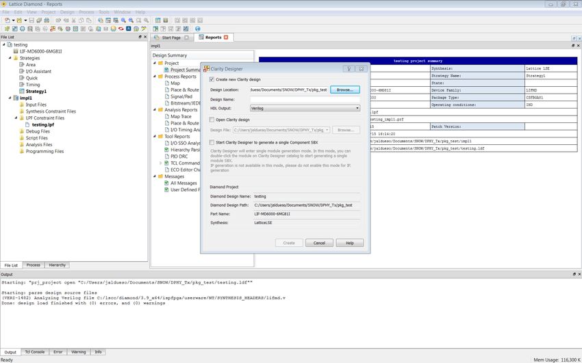
CSI-2/DSI D-PHY Transmitter Submodule IP
                                                                                                                                                                 User Guide

Figures
Figure 2.1. CSI-2/DSI D-PHY Transmitter Submodule Top Level Block Diagram ................................................................... 6
Figure 2.2. D-PHY Tx Input Bus for Short Packet Transmission ............................................................................................ 8
Figure 2.3. D-PHY Tx Input Bus for Long Packet Transmission in CSI-2 Interface ................................................................. 9
Figure 2.4. D-PHY Tx Input Bus for Long Packet Transmission in DSI Interface .................................................................... 9
Figure 2.5. D-PHY Tx Input Bus for Long Packet Transmission in DSI/CSI-2 Interface without pkt_formatter ..................... 9
Figure 2.6. High-Speed Data Transmission ......................................................................................................................... 10
Figure 2.7. Clock Domain Crossing Block Diagram.............................................................................................................. 11
Figure 2.8. D-PHY Transmitter Submodule Block Diagram ................................................................................................. 12
Figure 4.1. Clarity Designer Window .................................................................................................................................. 16
Figure 4.2. Starting Clarity Designer from Diamond Design Environment ......................................................................... 17
Figure 4.3. Configuring D-PHY Transmitter IP in Clarity Designer ...................................................................................... 18
Figure 4.4. Configuration Tab in IP User Interface .............................................................................................................. 19
Figure 4.5. Protocol Timing Parameter Tab in IP User Interface ........................................................................................ 20
Figure 4.6. D-PHY Transmitter IP Directory Structure ........................................................................................................ 20
Figure 4.7. Simulation Environment Block Diagram ........................................................................................................... 23
Figure 4.8 D-PHY Tx configured as CSI-2 Transmitter ......................................................................................................... 23
Figure 4.9. D-PHY Tx configured as DSI Transmitter ........................................................................................................... 24
Figure 4.10. IP Regeneration in Clarity Designer ................................................................................................................ 25

Tables
Table 1.1. CSI-2/DSI D-PHY Transmitter Submodule IP Quick Facts ..................................................................................... 4
Table 1.2. CSI-2/DSI D-PHY Transmitter Submodule IP Features Summary ......................................................................... 4
Table 2.1. D-PHY Transmitter Submodule IP Pin Function Description ................................................................................ 6
Table 2.2. Byte Data Bus Assignments ................................................................................................................................ 10
Table 2.3. Clock Domain Crossing ....................................................................................................................................... 11
Table 2.4 D-PHY Transmitter Top Level Parameter List ...................................................................................................... 12
Table 3.1. CSI-2/DSI D-PHY Tx Submodule IP Parameter Settings in User Interface .......................................................... 14
Table 3.2. CSI-2/DSI D-PHY Tx Submodule IP Compiler Directives ..................................................................................... 15
Table 4.1. Files Generated in Clarity Designer .................................................................................................................... 21
Table 4.2. Testbench Compiler Directives .......................................................................................................................... 22
Table A.1. Resource Utilization1 ......................................................................................................................................... 27

                    © 2017-2019 Lattice Semiconductor Corp. All Lattice trademarks, registered trademarks, patents, and disclaimers are as listed at www.latticesemi.com/legal.
       All other brand or product names are trademarks or registered trademarks of their respective holders. The specifications and information herein are subject to change without notice.

FPGA-IPUG-02024-1.1                                                                                                                                                                            3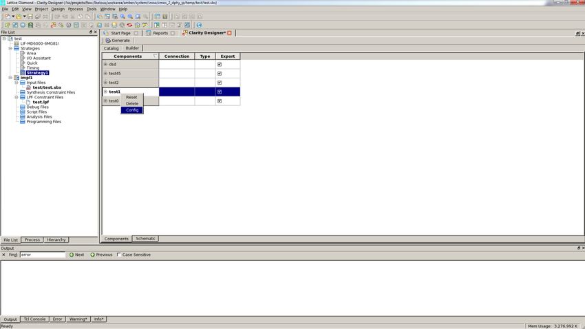
CSI-2/DSI D-PHY Transmitter Submodule IP
User Guide
1. Introduction
The Lattice Semiconductor CSI-2/DSI D-PHY Transmitter Submodule IP converts 64-bit data to either DSI or CSI-2 data
for Lattice Semiconductor CrossLink™ devices. This is useful for wearable, tablet, human-machine interfacing, medical
equipment and other applications.
Mobile Industry Processor Interface (MIPI®) D-PHY has become the industry’s primary high-speed PHY solution for
camera and display interconnection in mobile devices. It is typically used in conjunction with MIPI Camera Serial
Interface-2 (CSI-2) and MIPI Display Serial Interface (DSI) protocol Specifications. It meets requirements of low-power,
low-noise generation, and high-noise immunity that mobile phone designs demand.
This user guide is for CSI-2/DSI D-PHY Transmitter Submodule IP design version 1.x.
1.1. Quick Facts
Table 1.1 provides quick facts about the CSI-2/DSI D-PHY Transmitter Submodule IP for CrossLink device.
Table 1.1. CSI-2/DSI D-PHY Transmitter Submodule IP Quick Facts
D-PHY Transmitter Submodule IP Configuration
CSI-2 4-Lane DSI 4-Lane
IP Requirements FPGA Families Supported CrossLink
Targeted Device LIF-MD6000-6MG81I
Data Path Width 64-bit 64-bit
LUTs* 1183 5139
Resource Utilization
sysMEM™ EBRs 0 0
Registers 387 547
HW MIPI Block 1 1
Lattice Implementation Lattice Diamond® 3.9
Lattice Synthesis Engine
Design Tool Support Synthesis
Synplify Pro® L-2016.09L
Simulation Aldec®
Active HDL™ 10.3 Lattice Edition
*Note: DSI packet formatter includes FIFO while CSI-2 packet formatter does not include FIFO.
1.2. Features
The key features of the CSI-2/DSI D-PHY Transmitter Submodule IP include:
Compliant with MIPI DSI v1.1, MIPI CSI-2 v1.1 and MIPI D-PHY v1.1 Specifications
Supports MIPI DSI and MIPI CSI-2 interfacing up to 6 Gb/s
Supports 1, 2, or 4 MIPI D-PHY data lanes
Supports non-burst mode with sync events for transmission of DSI packets only
Supports low-power (LP) mode during vertical and horizontal blanking
Table 1.2. CSI-2/DSI D-PHY Transmitter Submodule IP Features Summary
IP Configuration Options
Number of Tx lanes 1, 2, 4
Gearing 8, 16
MIPI Interface DSI, CSI-2
© 2017-2019 Lattice Semiconductor Corp. All Lattice trademarks, registered trademarks, patents, and disclaimers are as listed at www.latticesemi.com/legal.
All other brand or product names are trademarks or registered trademarks of their respective holders. The specifications and information herein are subject to change without notice.
4 FPGA-IPUG-02024-1.1
CSI-2/DSI D-PHY Transmitter Submodule IP
User Guide
1.3. Conventions
1.3.1. Nomenclature
The nomenclature used in this document is based on Verilog HDL. This includes radix indications and logical operators.
1.3.2. Data Ordering and Data Types
The most significant bit within the pixel data is the highest index.
1.3.3. Signal Names
Signal names that end with:
_n are active low
_i are input signals
_o are output signals
_io are bidirectional signals
© 2017-2019 Lattice Semiconductor Corp. All Lattice trademarks, registered trademarks, patents, and disclaimers are as listed at www.latticesemi.com/legal.
All other brand or product names are trademarks or registered trademarks of their respective holders. The specifications and information herein are subject to change without notice.
FPGA-IPUG-02024-1.1 5CSI-2/DSI D-PHY Transmitter Submodule IP
User Guide
2. Functional Descriptions
The CSI-2/DSI D-PHY Transmitter Submodule IP converts 64-bit data to either DSI or CSI-2 byte packets. The input
interface consists of a 64-bit data arranged in CSI-2 or DSI data type format, a byte data enable, frame/vsync start
signal, line/hsync start signal, or short/long packet enable, virtual channel, data type, EoTP, word count and byte clock.
The output interface consists of serialized HS (High-speed) data packets following the MIPI CSI-2 or DSI Specifications. It
has a maximum of five lanes per channel (four data lanes and one clock lane only).
D-PHY Tx Wrapper D-PHY Tx Wrapper
(CSI-2 Interface) (DSI Interface)
reset_n_i clk_p_o reset_n_i clk_p_o
ref_clk_i Packet Tx Global D-PHY Common clk_n_o ref_clk_i Packet Tx Global D-PHY Common clk_n_o
pd_dphy_i Formatter Operation Interface d0_p_io pd_dphy_i Formatter Operation Interface d0_p_io
sp_en_i d0_n_io vsync_start_i d0_n_io
lp_en_i d1_p_o hsync_start_i d1_p_o
clk_hs_en_i PLL d1_n_o clk_hs_en_i PLL d1_n_o
d_hs_en_i d2_p_o d_hs_en_i d2_p_o
byte_data_en_i d2_n_o byte_data_en_i d2_n_o
byte_data_i[63:0] d3_p_o byte_data_i[63:0] d3_p_o
d3_n_o d3_n_o
D-PHY D-PHY
d_hs_rdy_o d_hs_rdy_o
byte_clk_o byte_clk_o
vc_i
dt_i vc_i
tinit_done_o tinit_done_o
wc_i dt_i
pll_lock_o pll_lock_o
wc_i
pix2byte_rstn_o pix2byte_rstn_o
eotp_i
D-PHY Tx Wrapper
(w/o pkt_formatter)
reset_n_i clk_p_o
ref_clk_i Packet Tx Global D-PHY Common clk_n_o
pd_dphy_i Formatter Operation Interface d0_p_io
clk_hs_en_i d0_n_io
d_hs_en_i d1_p_o
dphy_pkten_i PLL d1_n_o
dphy_pkt_i[63:0] d2_p_o
d2_n_o
d3_p_o
d3_n_o
D-PHY
d_hs_rdy_o
byte_clk_o
tinit_done_o
pll_lock_o
pix2byte_rstn_o
Figure 2.1. CSI-2/DSI D-PHY Transmitter Submodule Top Level Block Diagram
Table 2.1. D-PHY Transmitter Submodule IP Pin Function Description
Pin Name Direction Function Description
For DSI Interface
vsync_start_i1 I Start of vertical sync (pulse)
hsync_start_i1 I Start of horizontal sync (pulse)
For CSI-2 Interface
sp_en_i2 I Short packet enable (frame or line packet)
lp_en_i2 I Long packet enable
Byte Data Input
byte_data_i [63:0] Byte data
3 I
byte_data_en_i3 I Byte data enable
D-PHY Packet Input
dphy_pkt_i [63:0] 4 I D-PHY packet data
dphy_pkten_i4 I D-PHY packet enable
Common Interface
Asynchronous active low system reset.
reset_n_i I
0 – System is on reset
ref_clk_i I Reference clock for D-PHY PLL used to generate D-PHY serial clock and byte clock.
Power down input signal for D-PHY. When high, all D-PHY blocks are powered down. Tie low if
pd_dphy_i I
not used.
© 2017-2019 Lattice Semiconductor Corp. All Lattice trademarks, registered trademarks, patents, and disclaimers are as listed at www.latticesemi.com/legal.
All other brand or product names are trademarks or registered trademarks of their respective holders. The specifications and information herein are subject to change without notice.
6 FPGA-IPUG-02024-1.1CSI-2/DSI D-PHY Transmitter Submodule IP
User Guide
Pin Name Direction Function Description
vc_i [1:0]3 I Virtual channel ID
dt_i [5:0]3 I Data type
wc_i [15:0]3 I Word count in D-PHY packet
eotp_i1 I End of Transmission packet enable
clk_hs_en_i5 I Active high pulse going to the Tx Global operation to start LP to HS transition of clock lane
d_hs_en_i I Active high pulse going to the Tx Global operation to start LP to HS transition of data lane
d_hs_rdy_o O Active high signal to indicate data lane is ready for transmission
byte_clk_o O Byte clock generated by D-PHY PLL
d0_p_io I/O D-PHY data lane 0 Positive Data
d0_n_io I/O D-PHY data lane 0 Negative Data
d1_p_o O D-PHY data lane 1 Positive Data
d1_n_o O D-PHY data lane 1 Negative Data
d2_p_o O D-PHY data lane 2 Positive Data
d2_n_o O D-PHY data lane 2 Negative Data
d3_p_o O D-PHY data lane 3 Positive Data
d3_n_o O D-PHY data lane 3 Negative Data
clk_p_o O D-PHY clock lane Positive end
clk_n_o O D-PHY clock lane Negative end
Miscellaneous
tinit_done_o6 O tINIT done signal generated from IP
pll_lock_o6 O D-PHY PLL lock signal
pix2byte_rstn_o6 O Reset signal for pixel2byte FIFOs
Notes:
1. Enabled only for DSI interface (TX_DSI is defined).
2. Enabled only for CSI-2 interface (TX_CSI2 is defined).
lp_en_i is equivalent to the start of active line (long packet).
sp_en_i is equivalent to the start and end of frame or line (short packet).
3. Enabled when you need the packet formatter, and disabled when packet formatter is not needed.
4. Enabled when you do not need the packet formatter.
5. Enabled for non-continuous clock mode.
6. Can be turned-on when MISC_ON is defined.
© 2017-2019 Lattice Semiconductor Corp. All Lattice trademarks, registered trademarks, patents, and disclaimers are as listed at www.latticesemi.com/legal.
All other brand or product names are trademarks or registered trademarks of their respective holders. The specifications and information herein are subject to change without notice.
FPGA-IPUG-02024-1.1 7CSI-2/DSI D-PHY Transmitter Submodule IP
User Guide
2.1. Interface and Timing Diagram
2.1.1. Input Interface
2.1.1.1. Short Packet Transmission
Figure 2.2 shows the timing relationship between sp_en_i (frame and line short packets) for CSI-2 interface,
hsync/vsync start for DSI interface, and d_hs_en_i/clk_hs_en_i and d_hs_rdy_o signals for short packet transmission.
Short packet transmission is as follows:
1. Assert d_hs_en_i when you want to send a request for HS transmission. The clk_hs_en_i is not enabled for
continuous (HS_ONLY) clock mode. For non-continuous (HS_LP) clock mode, clk_hs_en_i needs to be asserted with
the d_hs_en_i.
2. Wait for d_hs_rdy_o to assert.
3. For CSI-2 interface, send one pulse of sp_en_i for every frame and line short packets. For DSI, send one pulse of
vsync_start_i or hsync_start_i. For every assertion of sp_en_i/ vsync_start_i/ hsync_start_i, the correct data type
should be provided.
byte_clk_o
d_hs_en_i /
clk_hs_en_i
d_hs_rdy_o
sp_en_i (CSI-2)
vsync_start_i /
hsync_start_i (DSI)
byte_data_en_i
byte_data_i[63:0]
dt_i[5:0]
Figure 2.2. D-PHY Tx Input Bus for Short Packet Transmission
2.1.1.2. Long Packet Transmission
Figure 2.3 and Figure 2.4 show the timing relationship between the lp_en_i (long packet enable), byte_data_en_i and
byte_data. Long packet transmission is as follows:
1. Assert d_hs_en_i when you want to send a request for HS transmission. The clk_hs_en_i is not enabled for
continuous (HS_ONLY) clock mode. For non-continuous (HS_LP) clock mode, clk_hs_en_i needs to be asserted with
the d_hs_en_i.
2. Wait for d_hs_rdy_o to assert.
3. For CSI-2 interface, send one pulse of lp_en_i for every frame and line short packets. For DSI, no flag signal is
needed.
4. Send byte_data_i together with the byte_data_en_i and the dt_i[5:0].
© 2017-2019 Lattice Semiconductor Corp. All Lattice trademarks, registered trademarks, patents, and disclaimers are as listed at www.latticesemi.com/legal.
All other brand or product names are trademarks or registered trademarks of their respective holders. The specifications and information herein are subject to change without notice.
8 FPGA-IPUG-02024-1.1CSI-2/DSI D-PHY Transmitter Submodule IP
User Guide
byte_clk_o
d_hs_en_i /
clk_hs_en_i
d_hs_rdy_o
lp_en_i
byte_data_en_i
byte_data_i[63:0]
dt_i[5:0]
Figure 2.3. D-PHY Tx Input Bus for Long Packet Transmission in CSI-2 Interface
byte_clk_o
d_hs_en_i /
clk_hs_en_i
d_hs_rdy_o
byte_data_en_i
byte_data_i[63:0]
dt_i[5:0]
Figure 2.4. D-PHY Tx Input Bus for Long Packet Transmission in DSI Interface
Figure 2.5 shows the timing diagram when you do not need the pkt_formatter anymore because data input is already
DSI/CSI-2 packets. After assertion of d_hs_en_i/clk_hs_en_i, wait for d_hs_rdy_o to assert and send the dphy_pkt_i
with the dphy_pkten_i.
byte_clk_o
d_hs_en_i /
clk_hs_en_i
d_hs_rdy_o
dphy_pkten_i
dphy_pkt_i[63:0]
Figure 2.5. D-PHY Tx Input Bus for Long Packet Transmission in DSI/CSI-2 Interface without pkt_formatter
© 2017-2019 Lattice Semiconductor Corp. All Lattice trademarks, registered trademarks, patents, and disclaimers are as listed at www.latticesemi.com/legal.
All other brand or product names are trademarks or registered trademarks of their respective holders. The specifications and information herein are subject to change without notice.
FPGA-IPUG-02024-1.1 9CSI-2/DSI D-PHY Transmitter Submodule IP
User Guide
Table 2.2. Byte Data Bus Assignments
4-Lane 2-Lane 1-Lane
Tx D-PHY Lanes byte_data_i
Gear 16 Gear 8 Gear 16 Gear 8 Gear 16 Gear 8
[7:0] Byte 1 Byte 1 Byte 1 Byte 1 Byte 1 Byte 1
Lane 0
[15:8] Byte 5 — Byte 3 — Byte 2 —
[23:16] Byte 2 Byte 2 Byte 2 Byte 2 — —
Lane 1
[31:24] Byte 6 — Byte 4 — — —
[39:32] Byte 3 Byte 3 — — — —
Lane 2
[47:40] Byte 7 — — — — —
[55:48] Byte 4 Byte 4 — — — —
Lane 3
[63:56] Byte 8 — — — — —
2.1.2. Output Interface
Figure 2.6 shows that prior to the HS mode data transfer, all clock and data lanes are in the LP11 state (1.2 V on the
P channel and 1.2 V on the N channel). The clock lane then goes to the LP01 state (0 V on the P channel and 1.2 V on
the N channel) followed by the LP00 state (0 V on the P channel and 0 V on the N channel). After that, the clock lane
goes into HS mode with SLVS200 signaling (Vcm=200 mV, Vdiff=±100 mV), and holds an HS0 state (differential 0 state
of P channel = 100 mV and N channel = 300 mV when termination of the receiver is turned on) according to
CMOS2DPHY IP Specifications. The clock starts shortly after. When the HS clock runs, the data lanes follow a similar
procedure going from LP11 to LP01, LP00, and HS0 states. The HS-SYNC sequence is driven on the line followed by the
packet header and data payload. At the end of the transfer the data lanes first go back into LP mode by going to LP00
then LP11 states. The clock lane follows shortly after.
Figure 2.6. High-Speed Data Transmission
2.2. Clock, Reset and Initialization
2.2.1. Reset and Initialization
After power-up, the transmitting D-PHY is required to drive a Stop State (LP-11) for a period longer than tINIT.
The D-PHY forces the lane module into transmit mode and generate stop state after system reset.
The Slave PHY is initialized when the Master PHY drives a Stop State (LP-11). The first Stop state that is longer than the
specified tINIT is called the Initialization period. tINIT is estimated to be minimum 100 μs.
An asynchronous reset pin (active high) is used for resetting the entire FPGA. Internal reset logic is implemented to
guarantee synchronous de-assertion throughout different clock domains for both hard and soft IPs. Unless specified by
MIPI IP or Soft IP requirement, no special reset sequence is needed for CrossLink. However, there is a wait time
requirement before the Application Processor can send valid data to the bridge. When set in DSI, until DCS ROM is done
© 2017-2019 Lattice Semiconductor Corp. All Lattice trademarks, registered trademarks, patents, and disclaimers are as listed at www.latticesemi.com/legal.
All other brand or product names are trademarks or registered trademarks of their respective holders. The specifications and information herein are subject to change without notice.
10 FPGA-IPUG-02024-1.1CSI-2/DSI D-PHY Transmitter Submodule IP
User Guide
sending the DCS commands to the display, valid data from the Application Processor might be lost. Likewise, for CSI-2,
until PLL is locked, valid data from the Application Processor might be lost.
2.2.2. Clock Domains and Clock Domain Crossing
The D-PHY PLL generates the bit clock from the input reference clock. Byte clock is then derived from this bit clock through
a clock generator inside the MIPI DPHY IP. Both the reference clock and byte clock are free-running.
Reference clock to the PLL should at least be 24 MHz based on the MIPI D-PHY PLL Specification. The maximum reference
clock is limited by the maximum fabric clock, 150 MHz.
D-PHY Tx Wrapper
Packet Tx Global D-PHY Common
Formatter Operation Interface
PLL byte_clk_o
clk_p_i
D-PHY clk_n_i
ref_clk_i
Figure 2.7. Clock Domain Crossing Block Diagram
Table 2.3. Clock Domain Crossing
Clock Domain Crossing Handling Approach
Byte clock to DPHY bit clock Hard D-PHY
The general formula for computing the required clocks of the system:
Tx line rate (total) = total pixels(active + blanking) ∗ frame rate ∗ bits per pixel
Tx line rate (total)
Tx line rate (per lane) =
no.of Tx lane
Tx line rate (per lane)
D-PHY clock =
2
D−PHY clock
Byte clock =
Tx gear/2
© 2017-2019 Lattice Semiconductor Corp. All Lattice trademarks, registered trademarks, patents, and disclaimers are as listed at www.latticesemi.com/legal.
All other brand or product names are trademarks or registered trademarks of their respective holders. The specifications and information herein are subject to change without notice.
FPGA-IPUG-02024-1.1 11CSI-2/DSI D-PHY Transmitter Submodule IP
User Guide
2.3. Design and Module Description
The top level module instantiates the Packet Formatter, Tx Global Operation, D-PHY Common Interface. There is an
option to instantiate the internal oscillator when you opt not to choose an external reference clock for the D-PHY PLL.
There is also an option to disable the packet formatter module when the byte_data_i already has the header and
footer.
D-PHY Tx Wrapper D-PHY Tx Wrapper
(CSI-2 Interface) (DSI Interface)
clk_p_o reset_n_i clk_p_o
reset_n_i Packet Tx Global D-PHY Common clk_n_o ref_clk_i Packet Tx Global D-PHY Common clk_n_o
ref_clk_i Formatter Operation Interface d0_p_io pd_dphy_i Formatter Operation Interface d0_p_io
pd_dphy_i d0_n_io vsync_start_i d0_n_io
sp_en_i d1_p_o hsync_start_i d1_p_o
lp_en_i PLL d1_n_o clk_hs_en_i PLL d1_n_o
clk_hs_en_i d2_p_o d_hs_en_i d2_p_o
d_hs_en_i d2_n_o byte_data_en_i d2_n_o
byte_data_en_i d3_p_o byte_data_i[63:0] d3_p_o
byte_data_i[63:0] d3_n_o d3_n_o
D-PHY D-PHY
d_hs_rdy_o d_hs_rdy_o
byte_clk_o byte_clk_o
vc_i
dt_i vc_i
tinit_done_o tinit_done_o
wc_i dt_i
pll_lock_o pll_lock_o
wc_i
pix2byte_rstn_o pix2byte_rstn_o
eotp_i
D-PHY Tx Wrapper
(w/o pkt_formatter)
reset_n_i clk_p_i
ref_clk_i Packet Tx Global D-PHY Common clk_n_i
pd_dphy_i Formatter Operation Interface d0_p_io
clk_hs_en_i d0_n_io
d_hs_en_i d1_p_o
dphy_pkten_i PLL d1_n_o
dphy_pkt_i[63:0] d2_p_o
d2_n_o
d3_p_o
d3_n_o
D-PHY
d_hs_rdy_o
byte_clk_o
tinit_done_o
pll_lock_o
pix2byte_rstn_o
Figure 2.8. D-PHY Transmitter Submodule Block Diagram
Table 2.4 D-PHY Transmitter Top Level Parameter List
Parameters Options Operation
T_LPX D-PHY Timing Parameters. Refer to Table 14 of MIPI D-PHY Specification v1.1 for
T_CLKPREP details.
T_CLK_HSZERO
T_CLKPRE
T_CLKPOST
T_CLKTRAIL
T_CLKEXIT
T_DATPREP
T_DAT_HSZERO
T_DATTRAIL
T_DATEXIT
FRAME_CNT_ENABLE ON The design automatically generates frame number. This is for non-D-PHY initiators.
OFF Users/Initiators generate the packet frame number via WC input port.
LINE_CNT_ENABLE ON The design automatically generates line number. This is for non-D-PHY initiators.
OFF Users/Initiators generate the packet line number via WC input port.
CLK_MODE HS_ONLY Tx D-PHY clock mode transmission.
HS_LP
TINIT_COUNT ON Enable or disable the tINIT counter inside the design to save utilization.
OFF
PKT_FORMAT ON Enable or disable packet formatter module.
© 2017-2019 Lattice Semiconductor Corp. All Lattice trademarks, registered trademarks, patents, and disclaimers are as listed at www.latticesemi.com/legal.
All other brand or product names are trademarks or registered trademarks of their respective holders. The specifications and information herein are subject to change without notice.
12 FPGA-IPUG-02024-1.1CSI-2/DSI D-PHY Transmitter Submodule IP
User Guide
Parameters Options Operation
OFF
CRC16 Enable or disable appending of 16-bit checksum to the end of packet. This is always
1
set to 1.
DATA_WIDTH 16 Always set to 16-bit data.
TINIT_VALUE D-PHY tINIT requirement
CN Tx PLL input divider
CM Tx PLL feedback divider
CO Tx PLL output divider
TX_FREQ_TGT Target Tx byte clock which is used in the D-PHY Tx global operation module.
PKTHDR_FIFO_IMPL LUT FIFO implementation of packet headers. This is always “LUT”.
EBR
LANE_WIDTH 1, 2, 4 Set the number of Tx D-PHY lanes.
GEAR_16 0, 1 Set the Tx gearing.
1 – 16:1 gearing
0 – 8:1 gearing
DSI_FORMAT 0, 1 Enable or disable DSI interface.
EOTP 0, 1 Appends end of transfer packet when enable.
The Packet Formatter block wraps the packet header and packet footer modules.
The Packet header module generates and appends the packet header and footer to the data payload.
The byte_data_en_i input and the byte_data_i bus are used together to identify when payload is available.
The header field and payload size is configurable by setting VC, WC, and DT parameters. End of Transmission Packet
(EoTP) is supported by this module. The Packet footer module computes a CRC16 checksum based on incoming data
and data enable. The data bus input is maximum 64 bits.
The Tx Global Operation block controls HS request path and timing using parameters. Currently LP-request, escape
mode and turnaround path are not supported. This block follows the requirements described D-PHY Specification
version 1.2 section 6 — operating modes for control and high-speed data transmission. DSI data goes into Lower-Power
mode during vertical and horizontal blanking depending on the Soft IP design.
Example: HS-0/1 -> LP11(Stop) -> LP01(LP-Rqst) -> LP00(Bridge) -> HS-0/1
This module controls the timing entering HS and coming from HS entering to LP following the MIPI D-PHY Specification
1.1 Table 14. The delay parameters can be adjusted inside this module by changing its local parameter.
The DCI (D-PHY Common Interface) wrapper is used as the wrapper of MIPI D-PHY IP to make a connection between
the PHY hard IP and higher protocol layers. The DCI wrapper serializes the incoming byte data and transmits it to D-PHY
receiver. Based on the Tx global operation state, it determines how to enable HS or LS mode for data transfer.
© 2017-2019 Lattice Semiconductor Corp. All Lattice trademarks, registered trademarks, patents, and disclaimers are as listed at www.latticesemi.com/legal.
All other brand or product names are trademarks or registered trademarks of their respective holders. The specifications and information herein are subject to change without notice.
FPGA-IPUG-02024-1.1 13CSI-2/DSI D-PHY Transmitter Submodule IP
User Guide
3. Compiler Directives and Parameter Settings
3.1. Parameters Settings
Table 3.1 lists the parameters used to generate the D-PHY Transmitter Submodule IP. All parameters are either set
automatically or input in the user interface during the D-PHY Transmitter Submodule IP generation.
Table 3.1. CSI-2/DSI D-PHY Tx Submodule IP Parameter Settings in User Interface
Parameter Attribute Options Description
Number of Tx Lanes User-Input 1, 2, 4 Generate I/O up to four HS Tx data lane.
Tx Interface User-Input DSI, CSI-2 Set the Tx interface.
Tx Gear Read-Only 8, 16 Set the Tx gearing.
Tx Line Rate Read-Only Target Tx line. Expected to be the same with Rx line rate.
Tx Line Rate (per lane) User-Input Target Tx line rate per lane.
D-PHY Clock Frequency Read-Only D-PHY clock; Automatically computed based on target Tx line rate.
Byte Clock Frequency Read-Only Byte clock; Automatically computed based on target Tx line rate.
Reference Clock Frequency User-Input Reference clock for D-PHY PLL. The D-PHY PLL, which is used to
generate the D-PHY clocks, should be programmed such that the
frequency after the input divider ranges from 24 MHz to 30 MHz
(24 ≤ (Reference Clock/N) ≤ 30), otherwise, Mixel PLL does not work.
Due to this requirement, there are frequency holes in the frequency
range supported by the design. It must satisfy the following
conditions:
Minimum of 24 MHz
Must not be between 30 MHz and 48 MHz
Must not be between 60 MHz and 72 MHz
Must not be between 90 and 96 MHz
Maximum of 150 MHz
tINIT_SLAVE Value User-Input Specify delay time for Tx D-PHY tINIT requirement. Must satisfy Tx
D-PHY tINIT minimum requirement of 100 μs and is clocked by byte
clock.
Disable tINIT counter User-Input Enable Enable or disable tINIT counter for resource utilization.
Disable
Disable Packet formatter User-Input Enable Enable or disable packet formatter module.
Disable
Enable Frame number User-Input Enable Enable or disable frame number increment in packet formatter for
increment Disable CSI-2 interface.
Enable Line number User-Input Enable Enable or disable line number increment in packet formatter for
increment Disable CSI-2 interface.
TLPX User-Input D-PHY Global Operation Timing parameters. Refer to section 6.9 of
Clock Prepare MIPI D-PHY Specification v1.1.
Clock HS-zero
Clock Pre
Clock Post
Clock Trail
Clock Exit
Data Prepare
Data HS-zero
Data Trail
Data Exit
© 2017-2019 Lattice Semiconductor Corp. All Lattice trademarks, registered trademarks, patents, and disclaimers are as listed at www.latticesemi.com/legal.
All other brand or product names are trademarks or registered trademarks of their respective holders. The specifications and information herein are subject to change without notice.
14 FPGA-IPUG-02024-1.1CSI-2/DSI D-PHY Transmitter Submodule IP
User Guide
3.2. Compiler Directives
Table 3.2. CSI-2/DSI D-PHY Tx Submodule IP Compiler Directives
Compiler Directive Options Description
NUM_TX_LANE_1 1
NUM_TX_LANE_2 2 Generate D-PHY Tx I/O.
NUM_TX_LANE_4 4
TX_GEAR_8 8
Set the Tx gearing.
TX_GEAR_16 16
TX_DSI DSI
Set the MIPI interface.
TX_CSI2 CSI-2
CM (640CSI-2/DSI D-PHY Transmitter Submodule IP
User Guide
4. IP Generation and Evaluation
This section provides information on how to generate the Lattice D-PHY Transmitter Submodule IP code using the
Lattice Diamond Clarity Designer and how to run simulation, synthesis and hardware evaluation.
4.1. Licensing the IP
The D-PHY Transmitter IP is available free of charge, but an IP-specific license is required to enable full, unrestricted use
of the D-PHY Transmitter IP in a complete, top level design.
Request your license by going to the link http://www.latticesemi.com/en/Support/Licensing and request the free
Lattice Diamond license. In this form, select the desired CrossLink IP for your design.
You may download and generate the D-PHY Transmitter IP and fully evaluate the IP through functional simulation and
implementation (synthesis, map, place and route) without an IP license. The D-PHY Transmitter IP also supports
Lattice’s IP hardware evaluation capability, see the Hardware Evaluation section for further details.
HOWEVER, THE IP LICENSE IS REQUIRED TO ENABLE TIMING SIMULATION, TO OPEN THE DESIGN IN DIAMOND EPIC
TOOL, OR TO GENERATE BITSTREAMS THAT DO NOT INCLUDE THE HARDWARE EVALUATION TIMEOUT LIMITATION.
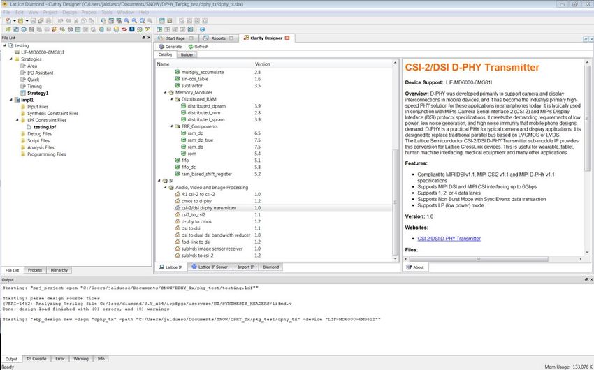
4.2. Getting Started
The D-PHY Transmitter IP is available for download from the Lattice IP Server using the Clarity Designer tool. The IP files
are automatically installed using ispUPDATE technology in any customer-specified directory. After the IP is installed,
the IP is available in the Clarity Designer user interface as shown in Figure 4.1.
Figure 4.1. Clarity Designer Window
© 2017-2019 Lattice Semiconductor Corp. All Lattice trademarks, registered trademarks, patents, and disclaimers are as listed at www.latticesemi.com/legal.
All other brand or product names are trademarks or registered trademarks of their respective holders. The specifications and information herein are subject to change without notice.
16 FPGA-IPUG-02024-1.1CSI-2/DSI D-PHY Transmitter Submodule IP
User Guide
4.3. Generating IP in Clarity Designer
The Clarity Designer tool is used to customize modules and IPs and place them into the device’s architecture. Besides
configuration and generation of modules and IPs, Clarity Designer can also create a top module template in which all
generated modules and IPs are instantiated.
The procedure for generating D-PHY Transmitter IP in Clarity Designer is described below.
Clarity Designer can be started from the Diamond design environment.
To start Clarity Designer:
1. Create a new Diamond project for CrossLink family devices.
2. From the Diamond main window, choose Tools > Clarity Designer, or click in Diamond toolbox. The Clarity
Designer project dialog box is displayed.
3. Select and/or fill out the following items as shown in Figure 4.2.
Create new Clarity design – Click this to create a new Clarity Design project directory in which the D-PHY
Transmitter IP will be generated.
Design Location – Clarity Design project directory path.
Design Name – Clarity Design project name.
HDL Output – Hardware Description Language Output Format (Verilog).
The Clarity Designer project dialog box also allows you to open an existing Clarity Designer project by selecting the
following:
Open Clarity design – Open an existing Clarity Design project.
Design File – Name of existing Clarity Design project file with .sbx extension.
4. Click the Create button. A new Clarity Designer project is created.
Figure 4.2. Starting Clarity Designer from Diamond Design Environment
© 2017-2019 Lattice Semiconductor Corp. All Lattice trademarks, registered trademarks, patents, and disclaimers are as listed at www.latticesemi.com/legal.
All other brand or product names are trademarks or registered trademarks of their respective holders. The specifications and information herein are subject to change without notice.
FPGA-IPUG-02024-1.1 17CSI-2/DSI D-PHY Transmitter Submodule IP
User Guide
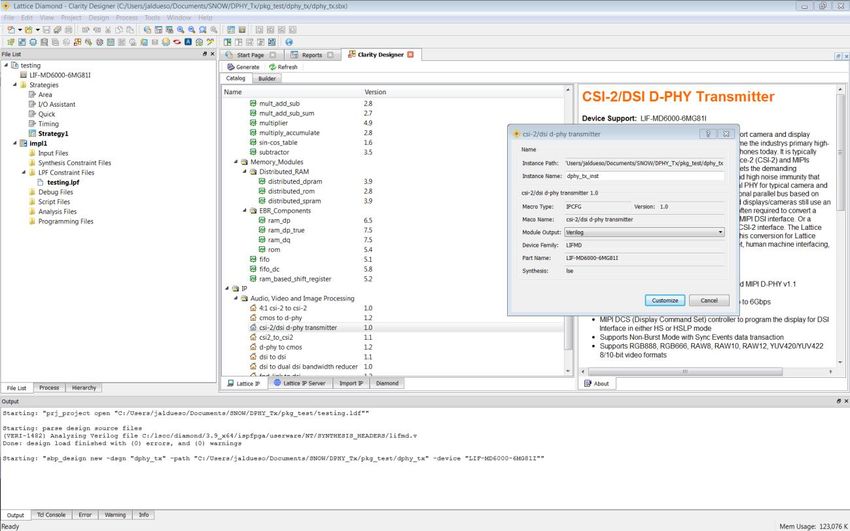
To configure D-PHY Transmitter IP in Clarity Designer:
1. Double-click csi-2/dsi d-phy transmitter in the IP list of the System Catalog view. The csi-2/dsi d-phy transmitter
dialog box is displayed as shown in Figure 4.3.
Figure 4.3. Configuring D-PHY Transmitter IP in Clarity Designer
2. Enter the Instance Name.
3. Click the Customize button. An IP configuration interface is displayed as shown in Figure 4.4. From this dialog box,
you can select the IP configuration specific to your application.
4. Input valid values in the required fields in the Configuration tab.
© 2017-2019 Lattice Semiconductor Corp. All Lattice trademarks, registered trademarks, patents, and disclaimers are as listed at www.latticesemi.com/legal.
All other brand or product names are trademarks or registered trademarks of their respective holders. The specifications and information herein are subject to change without notice.
18 FPGA-IPUG-02024-1.1CSI-2/DSI D-PHY Transmitter Submodule IP
User Guide
Figure 4.4. Configuration Tab in IP User Interface
5. Go to Protocol Timing Parameters tab. The values shown are automatically computed. You can enter other valid
values if customization is desired.
6. After selecting the required parameters, click the Configure button.
7. Click Close.
8. Click in the toolbox. Clarity Designer generates all the IPs and modules, and creates a top module to
wrap them.
For detailed instructions on how to use the Clarity Designer, refer to the Lattice Diamond software user guide.
© 2017-2019 Lattice Semiconductor Corp. All Lattice trademarks, registered trademarks, patents, and disclaimers are as listed at www.latticesemi.com/legal.
All other brand or product names are trademarks or registered trademarks of their respective holders. The specifications and information herein are subject to change without notice.
FPGA-IPUG-02024-1.1 19CSI-2/DSI D-PHY Transmitter Submodule IP
User Guide
Figure 4.5. Protocol Timing Parameter Tab in IP User Interface
4.4. Generated IP Directory Structure and Files
Figure 4.6 shows the directory structure of generated IP and supporting files.
Figure 4.6. D-PHY Transmitter IP Directory Structure
© 2017-2019 Lattice Semiconductor Corp. All Lattice trademarks, registered trademarks, patents, and disclaimers are as listed at www.latticesemi.com/legal.
All other brand or product names are trademarks or registered trademarks of their respective holders. The specifications and information herein are subject to change without notice.
20 FPGA-IPUG-02024-1.1CSI-2/DSI D-PHY Transmitter Submodule IP
User Guide
The design flow for the IP created with Clarity Designer uses a post-synthesized module (NGO) for synthesis and a
protected model for simulation. The post-synthesized module and protected model are customized when you
configure the IP and created automatically when the IP is generated.
Table 4.1 provides a list of key files and directories created by Clarity Designer and how they are used. The
post-synthesized module (NGO), the protected simulation model, and all other files are also generated based on your
configuration and are provided as examples to use or evaluate the IP.
Table 4.1. Files Generated in Clarity Designer
File Description
.v Verilog top-level module of D-PHY Transmitter IP used for both synthesis and simulation.
Verilog submodules for simulation. Files that do not have equivalent black box modules are also
_*.v
used for synthesis.
_*_beh.v Protected Verilog models for simulation.
_* _bb.v Verilog black box modules for synthesis.
_*.ngo User interface configured and synthesized modules for synthesis.
Verilog parameters file which contains required compiler directives to successfully configure IP
_params.v
during synthesis and simulation.
Lattice Parameters Configuration file. This file records all the IP configuration options set through
Clarity Designer. It is used by IP generation script to generate configuration-specific IP. It is also
.lpc
used to reload parameter settings in the IP user interface in Clarity Designer when it is being
reconfigured.
_inst.v/vhd Template for instantiating the generated soft IP top-level in another user-created top module.
Aside from the files listed in the tables, most of the files required to evaluate the D-PHY Transmitter IP are available
under the directory \. This includes the simulation model. Lattice Diamond project files are also included
under the folder at \\\impl\lifmd\\.
The \ folder contains files/folders with content specific to the configuration. This
directory is created by Clarity Designer each time the IP is generated and regenerated with the same file name. A
separate \ directory is generated for IPs with different names, such as \,\, and
others.
The folder\, the \dphytx_eval and sub directories provide files supporting D-PHY Transmitter IP
evaluation that includes files/folders with content that is constant for all configurations of the D-PHY Transmitter IP.
The \dphytx_eval directory is created by Clarity Designer the first time the IP is generated, when multiple D-PHY
Transmitter IPs are generated in the same root directory and updated each time the IP is regenerated.
You can use the prebuilt Diamond projects provided at
\\dphytx_eval\\impl\lifmd\\ to evaluate the implementation
(synthesis, map, place and route) of the IP in Lattice Diamond tool. The src directory contains the behavioral models of
the black-boxed modules and the models directory provides library elements.
© 2017-2019 Lattice Semiconductor Corp. All Lattice trademarks, registered trademarks, patents, and disclaimers are as listed at www.latticesemi.com/legal.
All other brand or product names are trademarks or registered trademarks of their respective holders. The specifications and information herein are subject to change without notice.
FPGA-IPUG-02024-1.1 21CSI-2/DSI D-PHY Transmitter Submodule IP
User Guide
4.5. Running Functional Simulation
To run simulations using Active-HDL:
1. Under the Tools menu in Diamond, select Active-HDL.
2. In Active-HDL window, under the Tools tab, select Execute Macro.
3. Select the .do file \\dphytx_eval\\sim\aldec\*_run.do.
4. Click OK.
5. Wait for simulation to finish.
6. To override default TB parameters, modify the \\dphytx_eval\testbench\tb_setup_params.v file.
Table 4.2. Testbench Compiler Directives
Compiler Directive Description
NUM_BYTES Number of bytes per line
NUM_LINES Number of lines per frame
NUM_FRAMES Number of frames to be transmitted
DATA_TYPE 6-bits value of data type to be transmitted
DEBUG_ON Enable debug messages
EOTP_ENABLE Enable EoTP in DSI mode
LS_LE_EN Enable model transmission of LS and LE short packet in CSI-2 mode
VIRTUAL_CHANNEL Set virtual channel
HSYNC_PULSE_FRONT Number of HSYNC pulses before data transmission
HSYNC_PULSE_BACK Number of HSYNC pulses after data transmission
HS_RDY_NEG_TO_HS_CLK_EN_DLY Delay from d_hs_en negation to next d_hs_rdy_o assertion
HS_RDY_TO_BYTE_DATA_EN_DLY Delay from d_hs_en assertion to byte_data_en assertion
HS_RDY_TO_DPHY_PKTEN_DLY Delay from d_hs_en assertion to dphy_pkten assertion
HS_RDY_TO_HSYNC_START_DLY Delay from d_hs_en assertion to hsync_start assertion
HS_RDY_TO_VSYNC_START_DLY Delay from d_hs_en assertion to vsync_start assertion
HS_RDY_TO_LP_EN_DLY Delay from d_hs_en assertion to lp_en assertion
HS_RDY_TO_SP_EN_DLY Delay from d_hs_en assertion to sp_en assertion
LP_EN_TO_BYTE_DATA_EN_DLY Delay from lp_en pulse to byte_data_en assertion
HSYNC_TO_HSYNC_DLY Delay from hsync to next hsync packet transmission
VSYNC_TO_HSYNC_DLY Delay from vsync to next hsync packet transmission
Used when MISC_ON is not defined. This is for setting the wait time duration (in ps) of
TINIT_DURATION
tINIT ROM done.
© 2017-2019 Lattice Semiconductor Corp. All Lattice trademarks, registered trademarks, patents, and disclaimers are as listed at www.latticesemi.com/legal.
All other brand or product names are trademarks or registered trademarks of their respective holders. The specifications and information herein are subject to change without notice.
22 FPGA-IPUG-02024-1.1CSI-2/DSI D-PHY Transmitter Submodule IP
User Guide
4.6. Simulation Strategies
This section describes the simulation environment which demonstrates basic D-PHY Transmitter functionality.
Figure 4.7 shows the block diagram of simulation environment.
Figure 4.7. Simulation Environment Block Diagram
4.7. Simulation Environment
The simulation environment is made up of an input driver instance connected to the input of CSI-2/DSI D-PHY
Transmitter IP Core instance in the testbench. The input driver is configured based on CSI-2/DSI D-PHY Transmitter IP
Core configurations and testbench parameters. It can be configured to drive data up to 8 bytes per clock cycle
depending on the number of D-PHY Tx lanes and Tx gearing.
The input driver can also be configured to drive control signals specific to DSI and CSI-2. If miscellaneous signals are
enabled, the testbench waits for tinit_done assertion before transmitting byte data. Otherwise, a user-configurable
delay (tinit_duration) can be used to ensure that initialization is done before testbench transmits byte data. Refer to
the tb_setup_params.v file for different testbench parameters that can be used to control the simulation.
Figure 4.8 shows the CSI-2/DSI D-PHY Transmitter IP core configured as CSI-2 transmitter. Packet transmissions are
controlled by driving sp_en for short packets such as frame start, frame end, line start and line end packets. The lp_en
signal is used to drive data packets together with byte_data_en, byte_en and other control signals.
Figure 4.8 D-PHY Tx configured as CSI-2 Transmitter
Figure 4.9 shows the D-PHY Transmitter IP core configured as DSI transmitter. Sync packets are controlled by driving
vsync_start, hsync_start signals. Data transmissions are controlled by driving byte_data_en, byte_data input bus with
other control signals.
© 2017-2019 Lattice Semiconductor Corp. All Lattice trademarks, registered trademarks, patents, and disclaimers are as listed at www.latticesemi.com/legal.
All other brand or product names are trademarks or registered trademarks of their respective holders. The specifications and information herein are subject to change without notice.
FPGA-IPUG-02024-1.1 23CSI-2/DSI D-PHY Transmitter Submodule IP
User Guide
Figure 4.9. D-PHY Tx configured as DSI Transmitter
4.8. Instantiating the IP
The core modules of the CSI-2/DSI D-PHY Transmitter IP are synthesized and provided in NGO format with black box
Verilog source files for synthesis. A Verilog source file named _dphy_tx.v instantiates the black box of
core modules. The top-level file .v instantiates _dphy_tx.v.
A Verilog instance template _inst.v or VHDL instance template _inst.vhd is also
provided as a guide if the design is to be included in another top level module.
You do not need to instantiate the IP instances one by one manually. The top-level file and the other Verilog source
files are provided in \. These files are refreshed each time the IP is regenerated.
4.9. Synthesizing and Implementing the IP
In Clarity Designer, the Clarity Designer project file (.sbx) is added to Lattice Diamond as a source file after all IPs are
generated. Note that default Diamond strategy (.sty) and default Diamond preference file (.lpf) are used. When using
the .sbx approach, import the recommended strategy and preferences from
\\dphytx_eval\\impl\lifmd\lse or
\\dphytx_eval\\impl\lifmd\synplify directories. All required files are invoked
automatically. You can directly synthesize, map and place/par the design in the Diamond design environment after the
cores are generated.
Push-button implementation of this top-level design with either Synplify or Lattice Synthesis Engine is supported via
the Diamond project files _top.ldf which is located in the
\\dphytx_eval\\impl\lifmd\\ directory.
To use the pre-built Diamond project files:
1. Choose File > Open > Project.
2. In the Open Project dialog box, browse to
\\dphytx_eval\\impl\lifmd\\.
3. Select and open _top.ldf. At this point, all of the files needed to support top-level synthesis and
implementation are imported to the project.
4. Select the Process tab in the left-hand user interface window.
5. Implement the complete design via the standard Diamond user interface flow.
© 2017-2019 Lattice Semiconductor Corp. All Lattice trademarks, registered trademarks, patents, and disclaimers are as listed at www.latticesemi.com/legal.
All other brand or product names are trademarks or registered trademarks of their respective holders. The specifications and information herein are subject to change without notice.
24 FPGA-IPUG-02024-1.1CSI-2/DSI D-PHY Transmitter Submodule IP
User Guide
4.10. Hardware Evaluation
The CSI-2/DSI D-PHY Transmitter IP supports Lattice’s IP hardware evaluation capability, so you can create versions of
the IP that operate in hardware for a limited period of time without requiring the request of an IP license. It may also
be used to evaluate the IP in hardware in user-defined designs.
4.10.1. Enabling Hardware Evaluation in Diamond
Choose Project > Active Strategy > Translate Design Settings. The hardware evaluation capability may be enabled or
disabled in the Strategy dialog box. It is enabled by default.
4.11. Updating/Regenerating the IP
The Clarity Designer interface allows you to update the local IPs from the Lattice IP server. The updated IP can be used
to regenerate the IP in the design. To change the parameters of the IP used in the design, the IP must also be
regenerated.
4.11.1. Regenerating an IP in Clarity Designer
To regenerate IP in Clarity Designer:
1. In the Builder tab, right-click the IP instance to be regenerated and select Config from the menu as shown in
Figure 4.10.
Figure 4.10. IP Regeneration in Clarity Designer
2. The IP Configuration user interface is displayed. Change the parameters as required and click the Configure button.
3. Click in the toolbox. Clarity Designer regenerates all the instances which are reconfigured.
© 2017-2019 Lattice Semiconductor Corp. All Lattice trademarks, registered trademarks, patents, and disclaimers are as listed at www.latticesemi.com/legal.
All other brand or product names are trademarks or registered trademarks of their respective holders. The specifications and information herein are subject to change without notice.
FPGA-IPUG-02024-1.1 25CSI-2/DSI D-PHY Transmitter Submodule IP
User Guide
References
For more information about CrossLink devices, refer to the CrossLink Family Data Sheet (FPGA-DS-02007).
For further information on interface standards, refer to:
MIPI Alliance Specification for D-PHY, version 1.1, November 7, 2011, www.mipi.org
MIPI Alliance Specification for Display Serial Interface, version 1.1, November 22, 2011, www.mipi.org
MIPI Alliance Specification for Camera Serial Interface 2 (CSI-2), version 1.1, July 18, 2012, www.mipi.org
Software documentation:
Clarity Designer User Guide
Lattice Diamond User Guide
Technical Support Assistance
Submit a technical support case through www.latticesemi.com/techsupport.
© 2017-2019 Lattice Semiconductor Corp. All Lattice trademarks, registered trademarks, patents, and disclaimers are as listed at www.latticesemi.com/legal.
All other brand or product names are trademarks or registered trademarks of their respective holders. The specifications and information herein are subject to change without notice.
26 FPGA-IPUG-02024-1.1You can also read


