UM11083 User Manual for LPCXpresso804 Board Rev. 1.0 - 9 February 2018 - User Manual - NXP Semiconductors
←
→
Page content transcription
If your browser does not render page correctly, please read the page content below
UM11083
  User Manual for LPCXpresso804 Board
  Rev. 1.0 — 9 February 2018                            User Manual

Document information
Info                   Content
Keywords               LPCXpresso804, OM40001, LPC804
Abstract               LPCXpresso804 User Manual
NXP Semiconductors                                                                                                LPCXpresso804
                                                                                                                                 User Manual

Revision history
Rev           Date         Description
1.0           20180209     First release

Contact information
For more information, please visit: http://www.nxp.com
For sales office addresses, please send an email to: salesaddresses@nxp.com
UM11083                              All information provided in this document is subject to legal disclaimers.        © NXP B.V. 2018. All rights reserved.

User Manual                                      Rev. 1.0 — 9 February 2018                                                                     2 of 16
NXP Semiconductors LPCXpresso804
User Manual
1. Introduction
The LPCXpresso family of boards provides a powerful and flexible development system
for NXP's Cortex-M MCUs. They can be used with a range of development tools, including
the MCUXpresso IDE. The LPCXpresso804 board is developed by NXP to enable
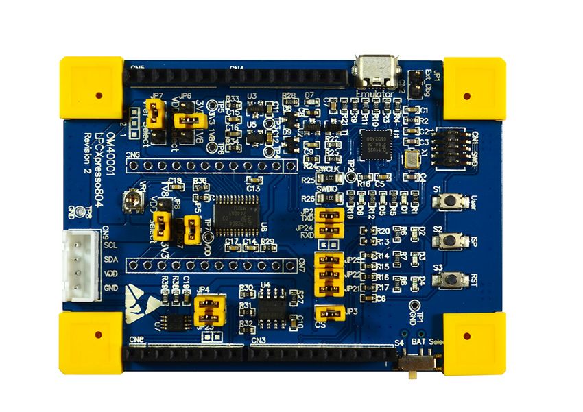
evaluation of and prototyping with the LPC804 MCU. Figure 1 shows the LPCXpresso804
main board. The board is also supplied with capacitive touch and PLU design prototyping
shield boards.
Fig 1. LPCXpresso804 Board
The LPCXpresso804 board includes the following features:
• Compatible with MCUXpresso IDE and other popular toolchains (incl. IAR and Keil)
• LPC804 Arm Cortex-M0+ MCU running at up to 15MHz
• On-board CMSIS-DAP (debug probe) with VCOM port, based on LPC11U35 MCU
• Debug connector to allow debug of target LPC804 MCU using an external probe
• LPC804 ISP and User/Wake buttons
• LPC804 Reset button
• 1Mb Winbond SPI flash
• NXP LM75BDP temperature sensor
• Programmable Logic Unit prototyping shield
• Capacitive Touch evaluation shield
• I2C Grove connector for easy connection of sensors, or to use the LPCXpresso804 as
an I/O expander peripheral
UM11083 All information provided in this document is subject to legal disclaimers. © NXP B.V. 2018. All rights reserved.
User Manual Rev. 1.0 — 9 February 2018 3 of 16NXP Semiconductors LPCXpresso804
User Manual
2. Board Layout
Figure 2 below shows the layout of the LPCXpresso804 board, indicating location of
jumpers, buttons and connectors/expansion options.
JP1
CN2
c
CN5 c
CN4
JP7
VREF
select Debug
CN1
probe LEDs
c
CN6
Pot S1
JP5
JP8 UART J2
VDD Jumpers JP24
select S2
CN9
JP4
c
CN7
JP22 S1
JP21
JP4
JP23 JP3
User LEDs
c
CN8 c
CN3
Fig 2. Board layout (top silkscreen)
Table 1 below shows the layout of the LPCXpresso804 board, indicating location of
jumpers, buttons, connectors/expansion options and MCU devices.
Table 1. Jumpers and connectors (LPCXpresso804 board)
Circuit reference Description Reference section
JP1 On-chip debug probe disable. Insert a jumper on this header to disable [4]
the on-board debug probe and use an external probe.
JP2 and JP24 LPC804 UART connections to debug probe. Remove these jumpers to [4]
disconnect the LPC804 UART port default (ISP) pins from the debug
probe (JP2 for PIO0_0 and JP24 for PIO0_4).
JP3 SPI flash select connection. Remove this jumper to disable the SPI flash [7.5]
for power measurement or to use the select signal pin for other purposes.
JP4 and JP23 Connections from SCL (JP4) and SDA (JP23) are routed from the LM75 [7.4]
to the LPC804 PIO0_14 and PIO0_7 via these jumpers. Remove the
jumpers during low power measurements or if these LPC804 pins are
being used for another function.
JP5 Install an ammeter across JP5 to measure current supplied to the LPC804 [6]
device. JP5 should be installed at all other times.
JP6 This jumper is not installed by default. It is provided for future support of See schematic.
dual rail versions of the LPC804.
UM11083 All information provided in this document is subject to legal disclaimers. © NXP B.V. 2018. All rights reserved.
User Manual Rev. 1.0 — 9 February 2018 4 of 16NXP Semiconductors LPCXpresso804
User Manual
Table 1. Jumpers and connectors (LPCXpresso804 board)
Circuit reference Description Reference section
JP7 ADC positive voltage reference (VREF). Selects between 3.3V and 1.8V See schematic.
for selection of the ADC voltage reference (default is 3.3V)
JP8 LPC804 VDD selection. Used to select between 3.3V and 1.8V supplies See schematic.
(default 3.3V)
JP21, JP22 and JP5 These jumpers are provided to allow the user LEDs to be disconnected See schematic.
from their respective LPC804 pins, enabling low power measurements
and for those signals to be used for other purposes. JP21, JP22 and JP25
enabled/disable PIO11, PIO_12 and PIO0_13 respectively.
CN2 USB connection for power and debug probe connection to host computer. [3][4]
CN3, CN4, CN5, CN8 Arduino connectors. [5.1]
CN6, CN7 Expansion / device pin access connectors. [5]
CN9 Grove I2C connector. [5.2]
VR1 (Pot) Potentiometer to provide an analog signal to the LPC804 ADC. See schematic.
UM11083 All information provided in this document is subject to legal disclaimers. © NXP B.V. 2018. All rights reserved.
User Manual Rev. 1.0 — 9 February 2018 5 of 16NXP Semiconductors LPCXpresso804
User Manual
3. Getting Started
This section describes how the operation of the factory programmed demo program, and
how to set up your board for code development with MCUXpresso IDE and/or third party
tools.
3.1 Initial setup and pre-programmed demo program
The LPCXpresso804 board is pre-programmed with a diagnostic demo program, which
tests various features of the board. This program utilizes the UART LPC804 output, which
is connected to the debug probe, which acts a serial to USB bridge to a host computer (as
well as providing the CMSIS-DAP debug interface.) To ensure a correct operation, a
VCOM serial port driver should be installed before powering the board when using
Windows 7 or 8 driver. This driver is available from http://nxp.com/demoboard/OM40001
under the Software and Tools tab (look under “Software” download types). After
downloading and unzipping the package, run the installer program provided to install the
driver (see installation notes included in the package for further information.)
Connect a micro USB cable from connector CN2 to a host computer or power supply to
power up the board and run the demo program. Open a terminal emulator program (such
as Teraterm or PuTTY), and look for a port with a name of the form “NXP LPC11Uxx
VCOM ...”, and connect to it. Set the serial port for 9600 baud, 8 bits, no parity.
• The Blue user LED will flash 3 times, then the green LED will flash 3 times, and the
terminal will display “HelloWorld”, followed by “Press key to start LED test ...”
• Press the ISP button (S2). The green and blue user LEDs will flash, then each LED
will be lit in turn twice before all three blink 3 times. The terminal will show “DONE”.
• The terminal will show “Press key to start SpiFlash test”. Press the ISP button. The
LEDs will blink as the test is run, and the SPI flash device ID and name will be shown
on the terminal.
• The terminal will show “Press key to start I2cTemperature test ...”. Press the ISP
button to run this test, which checks communication with the LM75 temperature
sensor.
• The terminal will show “Press key to start ADC Potentiometer test ...”. Press the ISP
button to run this test. The test checks the LPC804 ADC and potentiometer (VR1),
looking for the ADC reading to change at least once as it takes 6 samples over
several seconds. Use the supplied screwdriver to adjust VR1 so the test passes.
3.2 Using the board with MCUXpresso IDE
Once the device drivers have been installed (as described above), to use the board during
a debug session in MCUXpresso IDE, connect to the host computer then follow the steps
below.
The earliest version of MCUXpresso IDE that should be used is version 10.1.1. This
version does not have built-in knowledge of the LPC804 part family, so a patch needs to
be installed before attempting to use this board. The patch is available from the same
page as the MCUXpresso IDE download. From version 10.2 onwards (due for release in
Q2 2018) LPC804 will be built into the IDE and the patch will not be required.
UM11083 All information provided in this document is subject to legal disclaimers. © NXP B.V. 2018. All rights reserved.
User Manual Rev. 1.0 — 9 February 2018 6 of 16NXP Semiconductors LPCXpresso804
User Manual
Follow the steps below to build and run a simple example from the LPC804 Code Bundles
provided by NXP.
1. Code Bundles for the LPC8xx family are included in the MCUXpresso IDE installation.
These can also be downloaded from nxp.com (in case of any updates between IDE
releases):
http://www.nxp.com/products/software-and-tools/software-development-tools/softwar
e-tools/lpc800-code-bundles:LPC800-Code-Bundles.
2. Open a new workspace in the IDE.
3. In the Quickstart panel of the IDE, click in “Import a new project from the file system”
4. In the “Import project(s) from file system...” dialog box that opens, click “Browse...” in
the Project Archive (from zip) section, and select the LPC804 Code Bundle zip file
from the Code Bundles directory in the MCUXpresso IDE installation (or select a
version downloaded from nxp.com, as described in Step 1 above.) Click “Next >” on
the “Import project(s) from file system...” dialog to continue.
5. You will see several projects listed in the Code Bundle; click “Finish” to import them
all.
6. The dialog box will close, and you will see the imported projects in the Project tab at
the upper left window of the IDE. Click on Example_Multi_Timer_Blinky to select it,
then select Build from the Quickstart panel. You will see the build processing in the
Console window to the right of the Quickstart panel. The projects are set up to include
dependency checking, so the build process will automatically build the utility and
peripheral libraries as well as the example program.
7. Ensuring the LPCXpresso804 is connected to the host computer, click Debug in the
Quickstart panel. The IDE will search for available debug probes. Select the debug
probe that appears for your board, then click OK. Note that the IDE will remember
your selection for the next time you debug this project, so will not prompt for this
again, unless it cannot find the board.
8. The code will execute to main. Press F8 to resume and run the program. You will now
see the User LEDs light, each color in turn.
3.3 Using LPCXpresso804 with 3rd Party IDEs
Once the board device drivers have been installed (as described at the start of this
section), the board can be used with 3rd party development tools. Set up will vary
between Development Tools, but the board debug probe should supported as a
CMSIS-DAP probe in all cases).
Code Bundles, including sample projects for Keil MDK and IAR EWARM, are available
from NXP’s website at
http://www.nxp.com/products/software-and-tools/software-development-tools/software-to
ols/lpc800-code-bundles:LPC800-Code-Bundles. Refer to the readme files provided with
each code bundle in order to build/debug.
When using Keil MDK, install the Device Pack for the LPC804 (available for download
from within the Keil IDE) before attempting to use the board.
When using IAR EWARM, ensure that you have version 8.20.3 or later in order to have
LPC804 device family support.
UM11083 All information provided in this document is subject to legal disclaimers. © NXP B.V. 2018. All rights reserved.
User Manual Rev. 1.0 — 9 February 2018 7 of 16NXP Semiconductors LPCXpresso804
User Manual
3.4 Debugger firmware update (optional)
The MP board comes pre-programmed with a CMSIS-DAP firmware image; it is not
normally necessary to update the debugger firmware image, but this can be done by
following the steps below.
1. Hold down the reset button and keep it held down while applying power to the board.
Release reset. Using File Explorer (or equivalent on Mac/Linux platforms), look at the
available drives on your system. A device called CRP_DISABLED will appear.
2. Delete the firmware.bin file on the CRP_DISABLED drive.
3. Drag and drop the firmware.bin file you downloaded from nxp.com on to the
CRP_DISABLED drive.
4. Repower the board.
5. The board should now enumerate on your system - allow 20-30 seconds for this to
complete.
4. Debug Probe
LPCXpresso804 boards are factory programmed with a CMSIS-DAP compatible firmware
image, and a standard UART VCOM port. It should not be required to update the
LPC11U35 firmware, but Section 3.4 provides information on how to update the debug
probe firmware.
The CMSIS, DISK and COMM LEDs are connected to the LPC11U35 device. The
behavior of the LEDs will vary depending on firmware used, typically the CMSIS LED will
blink when debug communication is occurring, and the COMM LED will blink when data is
being transferred over the VCOMM port.
4.1 Using an external debug probe
An external debug probe that supports ARM’s SWD interface, such as a SEGGER J-Link
or PE Micro probe, can be used with the LPCXpresso804 board. The external probe must
be connected to header CN1. When an external debug probe is used, the on-board probe
must be held in reset by placing a jumper on JP1. It is recommended that JP1 is fitted
before powering the board.
5. Expansion connectors/headers
The LPCXpresso804 board provides an Arduino UNO R3 shield site and a Grove I2C
connector to add additional peripherals, sensors or other circuitry, including off-the-shelf
expansion boards; this section describes these options. All LPC804 signals are also
available on breakout headers CN6 and CN7. For further details please refer to the board
schematics.
UM11083 All information provided in this document is subject to legal disclaimers. © NXP B.V. 2018. All rights reserved.
User Manual Rev. 1.0 — 9 February 2018 8 of 16NXP Semiconductors LPCXpresso804
User Manual
5.1 Arduino UNO Rev 3 expansion connectors
The Arduino UNO Rev 3 compatible connectors provided on the LPCXpresso804 board
provide I2C, SPI, UART, PWM and analog function connections to shield boards that are
available from various 3rd part suppliers, or for customer use. The pin mappings are
shown in the tables below. Some connections are shared with other board features, as
shown (in addition to being available on breakout headers C6 and CN7.)
Table 2. Arduino expansion connector pin mappings (CN4)
Pin Arduino signal LPCXpresso804 Shared with
3 Reset (active low) Reset/PIO0_5 Reset button, SWD reset input
4 3.3V Regulator (U3) output -
5 5V To board regulator -
inputs (U3 and U5)
6 GND GND -
7 GND GND -
Table 3. Arduino expansion analog connector pin mappings (CN5)
Pin Arduino signal LPC804 pin Shared with
1 A0 PIO0_10 CN6, potentiometer
2 A1 PIO0_16 CN6, SPI flash chip select
3 A2 PIO0_17 CN6
4 A3 PIO0_7 CN7, CN3, Grove connector, LM75
5 A4 PIO0_4 CN6, CN8
6 A5 PIO0_1 CN7, SPI Flash (clk)
Table 4. Arduino expansion connector pin mappings (CN3)
Pin Arduino signal LPC804 pin Shared with
1 SCL PIO0_14 CN7, Grove connector, LM75
2 SDA PIO0_7 CN7, CN5, Grove connector, LM75
3 AREF AREF
4 GND GND
5 SPI SCK PIO0_1 User button, SPI flash
6 SPI MISO PIO0_9 CN7, SPI flash
7 SPI MOSI PIO0_8 CN7, SPI flash
8 SPI SSEL PIO0_15 CN7
9 PWM/GPIO PIO0_18 CN6
10 PWM/GPIO PIO0_20 CN7
Table 5. Arduino expansion connector pin mappings (CN8)
Pin Arduino signal LPC804 pin Shared with
2 PWM/GPIO PIO0_19 CN7
3 PWM/GPIO PIO0_11 CN6, blue user LED
4 PWM/GPIO PIO0_13 CN6, User button, red user LED
5 INT PIO0_21 CN6
UM11083 All information provided in this document is subject to legal disclaimers. © NXP B.V. 2018. All rights reserved.
User Manual Rev. 1.0 — 9 February 2018 9 of 16NXP Semiconductors LPCXpresso804
User Manual
Table 5. Arduino expansion connector pin mappings (CN8)
Pin Arduino signal LPC804 pin Shared with
6 INT PIO0_12 CN6, green user LED
7 UART TX PIO0_4 CN5, CN6, debug UART
8 UART RX PIO0_0 CN7, debug UART
Note that the default ports for ISP UART boot are connected to CN2.
5.2 Grove connector
The LPCXpresso804 board includes a header for connection of Seeed Studio Grove I2C
sensors. This header supplies the I2C connections plus 3.3V and ground.
6. Power supplies and supply current measurement
This section describes available power options for the board, and how current
consumption of the LPC804 can be measured.
6.1 Board powering options
The Board may be powered by the USB connector (CN2), via the Arduino connector (5V
input pin) or by a coin cell battery inserted into the holder on the underside of the board.
When using the coin cell battery switch S4 must be closed to connect the battery.
Protection diodes are provided to prevent any of the possible power sources from back
powering another. Note that the LPC11U3x debug probe can only be powered by USB.
The LPC804 is powered from either a 1.8V or 3.3V (default) regulator, the selection of the
voltage used is made using JP8. The remaining circuitry on the board is always powered
by the 3.3V regulator, with the LPC11U3x debug probe having its own 3.3V regulator.
6.2 LPC804 supply current measurement
JP5 is provided as an insertion point for an ammeter to measure current flow to that MCU.
This jumper is inserted in line between the center pin of JP8 and the VDD supply of the
LPC804. When an ammeter is not being used, a jumper should be installed on JP5.
7. Other board features
This section describes other board features not detailed elsewhere in this document.
7.1 ISP booting and the ISP button
The LPC804 can be forced into ISP boot mode by holding down the ISP button (S2) and
then holding and releasing the Reset button (S3). The ISP button is connected to LPC804
pin PIO0_12, which is also routed to the Arduino expansion connector and to the cathode
of the green user LED3. LPC804 pin PIO0_12 can be reconfigured by software so that the
button can be used by an application as a general purpose button (refer to the LPC804
User Manual).
UM11083 All information provided in this document is subject to legal disclaimers. © NXP B.V. 2018. All rights reserved.
User Manual Rev. 1.0 — 9 February 2018 10 of 16NXP Semiconductors LPCXpresso804
User Manual
7.2 User button
The User button (S1) is for general purpose use by LPC804 applications. It is connected
to a 10K ohm pullup to 3.3V, and to the LPC804 PIO0_13 pin. It is also shared with the red
User LED1.
7.3 User LEDs
Three users LEDs are provided on the board, one blue, one green and one red. The
anodes of the LEDs are connected together, then through a zero ohm resistor to the 3.3V
regulator output (each has its own current limit resistor in-line). Each LED has a jumper in
series with it (JP21, JP22 and JP25) to prevent leakage from the LPC804 pins through the
diodes if accurate power measurement measurements are being performed. All the PIOs
used for these LEDs are also shared with the Arduino expansion connector, but those
connections to the expansion connectors are not routed via the jumpers. The LEDs are
connected to the LPC804 as shown in the table below.
Table 6. User LED connections
LED LPC804 pin
Blue (D4) PIO0_11
Red (D3) PIO0_13
Green (D2) PIO0_12
7.4 Temperature sensor (LM75, circuit ref U7)
An NXP temperature sensor is included on the LPCXpresso804. This device interfaces to
the I2C peripheral of the LPC804, with an address of 0x1001100. Jumpers (JP4 and JP23)
are provided in-line with the SCL (PIO0_14) and SDA (PIO0_7) respectively so that this
device may be disconnected if not required.
7.5 SPI flash (Winbond W25X10CLSNIG, circuit ref U4)
A 1Mb SPI flash from Winbond is included on the LPCXpresso804. This device interfaces
to the SPI peripheral of the LPC804. A jumper (JP3) is provided to this device can be
disconnected (by disabling the SPI chip select PIO_16).
8. PLU Shield
The OM40001 package includes a shield board for use with the LPCXpresso804 board
when prototyping programmable logic unit (PLU) designs. The PLU shield provides the
following features to assist with this type of development:
• 5 slide switches to enable 5 possible PLU inputs to be connected to VDD (marked as
VCC on the Shield) or GND through a resistor (to set those inputs to a logic 1 or zero)
• 8 LEDs with jumpers to connect/disconnect possible PLU outputs for visual status
indication
• Push button option for momentary / edge signal inputs
• Low frequency oscillator with 1024Hz and 8Hz outputs
UM11083 All information provided in this document is subject to legal disclaimers. © NXP B.V. 2018. All rights reserved.
User Manual Rev. 1.0 — 9 February 2018 11 of 16NXP Semiconductors LPCXpresso804
User Manual
The PLU shield also includes a test circuit that can be used to implement a simple
continuity tester, for experimentation with the LPC804 ADC and DAC (requires some
shield board modification.)
Several signals from the LPC804 used on the PLU Shield are shared with other functions
on the main LPCXpresso804 board. Please review jumper settings on the
LPCXpresso804 board carefully before installing the PLU Shield.
The PLU can be programmed using a PLU Configuration tool, available to download for
free at https://www.nxp.com/demoboard/OM40001 under the Software and Tools tab.
8.1 PLU input options
On/off switches S1 through S5 connect possible PLU inputs to VDD or GND via a resistor,
enabling those inputs to be driven to a known, fixed state. PIO0_8 is connected to a push
button (S6) and a 100kohm pull up to VDD; PIO0_8 will be grounded when the button is
pressed. Table 7 below shows these connections.
Table 7. PLU input on/off switches
Switch LPC804 signal Notes
S1 PIO0_0 Also connected to debug UART. Remove JP2 to avoid conflicts
S2 PIO0_10 Shared with potentiometer. Move potentiometer to center position to
avoid conflicts.
S3 PIO0_11 Also connected to user LED; remove JP21 to disconnect LED
S4 PIO0_4 Also connected to debug UART. Remove JP24 to avoid conflicts
S5 PIO0_13 Also connected to user LED; remove JP25 to disconnect LED.
S6 PIO0_8 Also connected to SPI flash data input.
A digital oscillator circuit is also included on the Shield, with 1.024kHz and 8Hz outputs
available. LPC804 signal PIO0_1 can be connected to these oscillator signals in order to
provide a low speed clock to the flip-flops in the PLU block. The center pin (2) of JP12
connects to PIO0_1, so a jumper can be placed onto JP12 to connect this signal to the
required clock (see markings on the Shield silk screen.) An external clock can be provided
to the PLU by connecting it to the center pin of JP12.
8.2 PLU output options
On/off switches S1 through S5 connect possible PLU inputs to VDD or GND via a resistor,
enabling those inputs to be driven to a known, fixed state. PIO0_8 is connected to a push
button (S6) and a 100kohm pull up to VDD; PIO0_8 will be grounded when the button is
pressed. Table 7 below shows these connections.
Table 8. PLU shield LEDs
LED LPC804 Jumper installed Notes
signal to enable
D1 PIO0_15 JP6
D2 PIO0_16 JP7
D3 PIO0_10 JP8 Ensure S2 is in VCC position to use.
D4 PIO0_18 JP9
D5 PIO0_12 JP10 Also used for green User LED. Remove JP22 to
isolate.
UM11083 All information provided in this document is subject to legal disclaimers. © NXP B.V. 2018. All rights reserved.
User Manual Rev. 1.0 — 9 February 2018 12 of 16NXP Semiconductors LPCXpresso804
User Manual
Table 8. PLU shield LEDs
LED LPC804 Jumper installed Notes
signal to enable
D6 PIO0_20 JP11
D7 PIO0_7 JP4 I2C connections also used for LM75. Remove JP23
to isolate.
D8 PIO0_14 JP5 I2C connections also used for LM75. Remove JP23
to isolate.
8.3 DAC/ADC continuity tester circuit
The PLU shield includes a simple circuit to implement a continuity tester, as shown below.
By enabling PIO0_11 as a DAC output, a test signal can be driven to a circuit probe
connected to JP3, then the voltage at the voltage divider formed by R18 and R20 can be
measured using an LPC804 ADC input (PIO0_19). In order to use this circuit it is
recommended that R15 is removed and S3 set to the VCC position.
9. Capacitive Touch Shield
The OM40001 package includes a shield board for evaluation of the LPC804 capacitive
touch feature. The Capacitive Touch Shield provides the following features:
• 5 capacitive touch buttons
• 5 LEDs, available for user applications (typically to indicate a button press)
The connections for the capacitive touch buttons are shown in Table 9. As some signals
are shared with other functions, the jumpers shown in the table should be removed from
the LPCXpresso804 board when using the capacitive touch shield.
Table 9. Capacitive touch button signals
Button LPC804 I/O Capacitive touch signal Shared with / remove jumper
S1 PIO0_12 CAPT_X0 User LED / JP22
S2 PIO0_21 CAPT_X1
S3 PIO0_13 CAPT_X2 User LED / JP25
S4 PIO0_11 CAPT_X3 User LED / JP21
S5 PIO0_19 CAPT_X4
UM11083 All information provided in this document is subject to legal disclaimers. © NXP B.V. 2018. All rights reserved.
User Manual Rev. 1.0 — 9 February 2018 13 of 16NXP Semiconductors LPCXpresso804
User Manual
Table 9. Capacitive touch button signals
Button LPC804 I/O Capacitive touch signal Shared with / remove jumper
Common PIO0_7 CAPT_YL LM75 / JP23
Common PIO0_16 ACMP_I4 (not used by default) (not used)
Common PIO0_17 CAPT_YH
The five user LEDs are active low (on when control signal is at logic 0). The signal
assignments are shown in Table 10. Note that PI00_8 and PIO0_9 are also connected to
the SPI flash data inputs/outputs, so it is advisable to remove JP3 on the LPCXpresso804
board (to disable the SPI flash memory) before installing this shield board.
Table 10. Capacitive touch LED signals
LED LPC804 I/O
D1 PIO0_20
D2 PIO0_18
D3 PIO0_15
D4 PIO0_8
D5 PIO0_9
The LPC804 Code Bundle, available under the Software and Tools tab of the OM40001
board web page (http://www.nxp.com/demoboard/OM40001), includes driver and
example code to show how to use the capacitive touch feature of the board.
UM11083 All information provided in this document is subject to legal disclaimers. © NXP B.V. 2018. All rights reserved.
User Manual Rev. 1.0 — 9 February 2018 14 of 16NXP Semiconductors LPCXpresso804
User Manual
10. Legal information
10.1 Disclaimers Applications — Applications that are described herein for any of these
products are for illustrative purposes only. NXP Semiconductors makes no
representation or warranty that such applications will be suitable for the
Limited warranty and liability — Information in this document is believed to
specified use without further testing or modification.
be accurate and reliable. However, NXP Semiconductors does not give any
representations or warranties, expressed or implied, as to the accuracy or Customers are responsible for the design and operation of their applications
completeness of such information and shall have no liability for the and products using NXP Semiconductors products, and NXP Semiconductors
consequences of use of such information. accepts no liability for any assistance with applications or customer product
design. It is customer’s sole responsibility to determine whether the NXP
In no event shall NXP Semiconductors be liable for any indirect, incidental,
Semiconductors product is suitable and fit for the customer’s applications and
punitive, special or consequential damages (including - without limitation - lost
products planned, as well as for the planned application and use of
profits, lost savings, business interruption, costs related to the removal or
customer’s third party customer(s). Customers should provide appropriate
replacement of any products or rework charges) whether or not such
design and operating safeguards to minimize the risks associated with their
damages are based on tort (including negligence), warranty, breach of
applications and products.
contract or any other legal theory.
NXP Semiconductors does not accept any liability related to any default,
Notwithstanding any damages that customer might incur for any reason
damage, costs or problem which is based on any weakness or default in the
whatsoever, NXP Semiconductors’ aggregate and cumulative liability towards
customer’s applications or products, or the application or use by customer’s
customer for the products described herein shall be limited in accordance
third party customer(s). Customer is responsible for doing all necessary
with the Terms and conditions of commercial sale of NXP Semiconductors.
testing for the customer’s applications and products using NXP
Right to make changes — NXP Semiconductors reserves the right to make Semiconductors products in order to avoid a default of the applications and
changes to information published in this document, including without the products or of the application or use by customer’s third party
limitation specifications and product descriptions, at any time and without customer(s). NXP does not accept any liability in this respect.
notice. This document supersedes and replaces all information supplied prior
Export control — This document as well as the item(s) described herein
to the publication hereof.
may be subject to export control regulations. Export might require a prior
Suitability for use — NXP Semiconductors products are not designed, authorization from national authorities.
authorized or warranted to be suitable for use in life support, life-critical or
safety-critical systems or equipment, nor in applications where failure or
malfunction of an NXP Semiconductors product can reasonably be expected 10.2 Trademarks
to result in personal injury, death or severe property or environmental
damage. NXP Semiconductors accepts no liability for inclusion and/or use of Notice: All referenced brands, product names, service names and trademarks
NXP Semiconductors products in such equipment or applications and are the property of their respective owners.
therefore such inclusion and/or use is at the customer’s own risk.
UM11083 All information provided in this document is subject to legal disclaimers. © NXP B.V. 2018. All rights reserved.
User Manual Rev. 1.0 — 9 February 2018 15 of 16NXP Semiconductors LPCXpresso804
User Manual
11. Contents
1 Introduction . . . . . . . . . . . . . . . . . . . . . . . . . . . . 3
2 Board Layout . . . . . . . . . . . . . . . . . . . . . . . . . . . 4
3 Getting Started . . . . . . . . . . . . . . . . . . . . . . . . . . 6
3.1 Initial setup and pre-programmed demo program 6
3.2 Using the board with MCUXpresso IDE . . . . . . 6
3.3 Using LPCXpresso804 with 3rd Party IDEs . . . 7
3.4 Debugger firmware update (optional) . . . . . . . . 8
4 Debug Probe . . . . . . . . . . . . . . . . . . . . . . . . . . . 8
4.1 Using an external debug probe. . . . . . . . . . . . . 8
5 Expansion connectors/headers . . . . . . . . . . . . 8
5.1 Arduino UNO Rev 3 expansion connectors . . . 9
5.2 Grove connector . . . . . . . . . . . . . . . . . . . . . . . 10
6 Power supplies and supply current measurement 10
6.1 Board powering options . . . . . . . . . . . . . . . . . 10
6.2 LPC804 supply current measurement . . . . . . 10
7 Other board features . . . . . . . . . . . . . . . . . . . . 10
7.1 ISP booting and the ISP button . . . . . . . . . . . 10
7.2 User button . . . . . . . . . . . . . . . . . . . . . . . . . . . 11
7.3 User LEDs . . . . . . . . . . . . . . . . . . . . . . . . . . . 11
7.4 Temperature sensor (LM75, circuit ref U7) . . . 11
7.5 SPI flash (Winbond W25X10CLSNIG, circuit ref U4) 11
8 PLU Shield . . . . . . . . . . . . . . . . . . . . . . . . . . . . 11
8.1 PLU input options . . . . . . . . . . . . . . . . . . . . . . 12
8.2 PLU output options . . . . . . . . . . . . . . . . . . . . . 12
8.3 DAC/ADC continuity tester circuit . . . . . . . . . . 13
9 Capacitive Touch Shield . . . . . . . . . . . . . . . . . 13
10 Legal information. . . . . . . . . . . . . . . . . . . . . . . 15
10.1 Disclaimers . . . . . . . . . . . . . . . . . . . . . . . . . . . 15
10.2 Trademarks. . . . . . . . . . . . . . . . . . . . . . . . . . . 15
11 Contents . . . . . . . . . . . . . . . . . . . . . . . . . . . . . . 16
UM11083 All information provided in this document is subject to legal disclaimers. © NXP B.V. 2018. All rights reserved.
User Manual Rev. 1.0 — 9 February 2018 16 of 16You can also read