Power Delivery Network (PDN) Tool User Guide
←
→
Page content transcription
If your browser does not render page correctly, please read the page content below
Power Delivery Network (PDN) Tool User Guide

101 Innovation Drive
San Jose, CA 95134                                 Document Version:          2.0
www.altera.com                                     Document Date:      March 2009
Copyright © 2009 Altera Corporation. All rights reserved. Altera, The Programmable Solutions Company, the stylized Altera logo, specific device designations, and all other
words and logos that are identified as trademarks and/or service marks are, unless noted otherwise, the trademarks and service marks of Altera Corporation in the U.S. and other
countries. All other product or service names are the property of their respective holders. Altera products are protected under numerous U.S. and foreign patents and pending ap-
plications, maskwork rights, and copyrights. Altera warrants performance of its semiconductor products to current specifications in accordance with Altera's standard warranty,
but reserves the right to make changes to any products and services at any time without notice. Altera assumes no responsibility or liability arising out of the application or use of
any information, product, or service described herein except as expressly agreed to in writing by Altera Corporation. Altera customers are advised to obtain the latest version of
device specifications before relying on any published information and before placing orders for products or services.

                                                                                    UG-01036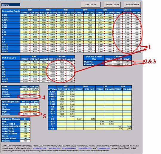
Contents

Chapter 1. Power Delivery Network (PDN) Tool User Guide
  Introduction . . . . . . . . . . . . . . . . . . . . . . . . . . . . . . . . . . . . . . . . . . . . . . . . . . . . . . . . . . . . . . . . . . . . . . . . . . . . 1-1
  Application of the Tool . . . . . . . . . . . . . . . . . . . . . . . . . . . . . . . . . . . . . . . . . . . . . . . . . . . . . . . . . . . . . . . . . . . 1-1
  PDN Decoupling Methodology Review . . . . . . . . . . . . . . . . . . . . . . . . . . . . . . . . . . . . . . . . . . . . . . . . . . . . 1-1
     PDN Circuit Topology . . . . . . . . . . . . . . . . . . . . . . . . . . . . . . . . . . . . . . . . . . . . . . . . . . . . . . . . . . . . . . . . . 1-1
  Setting Up the PDN Tool . . . . . . . . . . . . . . . . . . . . . . . . . . . . . . . . . . . . . . . . . . . . . . . . . . . . . . . . . . . . . . . . . 1-2
     Pre-Layout Instructions . . . . . . . . . . . . . . . . . . . . . . . . . . . . . . . . . . . . . . . . . . . . . . . . . . . . . . . . . . . . . . . . 1-3
     Tabs in the PDN Tool . . . . . . . . . . . . . . . . . . . . . . . . . . . . . . . . . . . . . . . . . . . . . . . . . . . . . . . . . . . . . . . . . . 1-9
  Summary . . . . . . . . . . . . . . . . . . . . . . . . . . . . . . . . . . . . . . . . . . . . . . . . . . . . . . . . . . . . . . . . . . . . . . . . . . . . . . 1-19
  Document Revision History . . . . . . . . . . . . . . . . . . . . . . . . . . . . . . . . . . . . . . . . . . . . . . . . . . . . . . . . . . . . Info-1
  How to Contact Altera . . . . . . . . . . . . . . . . . . . . . . . . . . . . . . . . . . . . . . . . . . . . . . . . . . . . . . . . . . . . . . . . . Info-1
  Typographic Conventions . . . . . . . . . . . . . . . . . . . . . . . . . . . . . . . . . . . . . . . . . . . . . . . . . . . . . . . . . . . . . . Info-2

© March 2009 Altera Corporation                                                                                   Power Delivery Network (PDN) Tool User Guide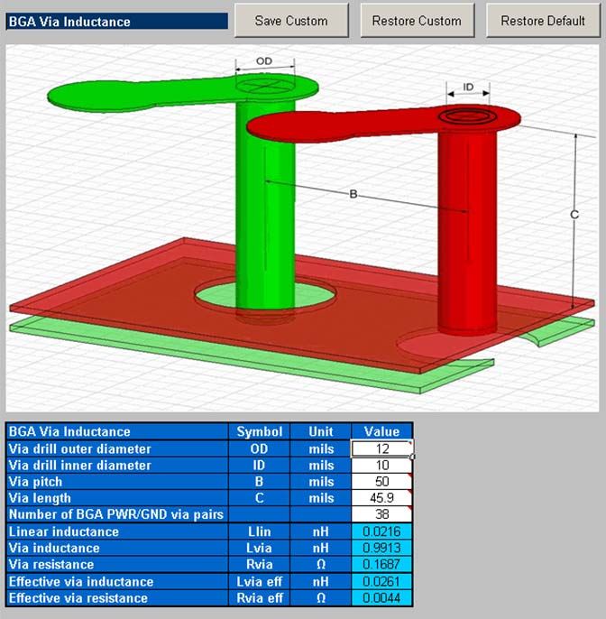
2

Power Delivery Network (PDN) Tool User Guide   © March 2009 Altera Corporation
1. Power Delivery Network (PDN) Tool
                                                                              User Guide

Introduction
                          PCB designers must estimate the number, value, and type of decoupling capacitors
                          required to develop an efficient PCB decoupling strategy during the early design
                          phase, without going through extensive pre-layout simulations. The Altera’s Power
                          Delivery Network (PDN) tool provides these critical pieces of information.
                          The PDN tool is a Microsoft Excel-based spreadsheet tool used to calculate an
                          impedance profile based on user inputs. For a given power supply, the spreadsheet
                          requires only basic design information, such as the board stackup, transient current
                          information, and ripple specifications to come up with the impedance profile and the
                          optimum number of capacitors to meet the desired impedance target. The results
                          obtained through the spreadsheet tool are intended only as a preliminary estimate
                          and not as a specification. For an accurate impedance profile, Altera® recommends a
                          post-layout simulation approach using any of the available EDA tools, such as Sigrity
                          PowerSI, Ansoft SIWave, Cadence Allegro PCB PI, etc.
                          This version of the PDN tool is a general purpose tool for helping with the PCB
                          decoupling design. Altera has family-specific PDN tools for its FPGA devices that
                          help reduce over-design in PCB decoupling by taking the effects of device-related
                          parameters into consideration.

               f          For the availability of the PDN tool that targets your device, refer to the Altera website
                          at www.altera.com.

Application of the Tool
                          The purpose of the tool is to design a robust power delivery network by determining
                          an optimum number, type, and value of decoupling capacitors required to meet the
                          desired target impedance up to the target frequency. This spreadsheet tool is useful
                          for exploring the various what-if scenarios during the early design phase, without
                          extensive and time consuming pre-layout analysis.

PDN Decoupling Methodology Review
                          The PDN tool is based on a lumped equivalent model representation of the power
                          delivery network topology. Figure 1–1 shows a schematic representation of the circuit
                          topology, modeled as part of the tool.

PDN Circuit Topology
                          For first order analysis, the voltage regulator module (VRM) can be simply modeled
                          as a series-connected resistor and inductor, as shown in Figure 1–1. At low
                          frequencies, up to approximately 50 KHz, the VRM has a very low impedance and is
                          capable of responding to the instantaneous current requirements of the FPGA. The
                          ESR and ESL values can be obtained from the VRM manufacturer.

© March 2009   Altera Corporation                                               Power Delivery Network (PDN) Tool User Guide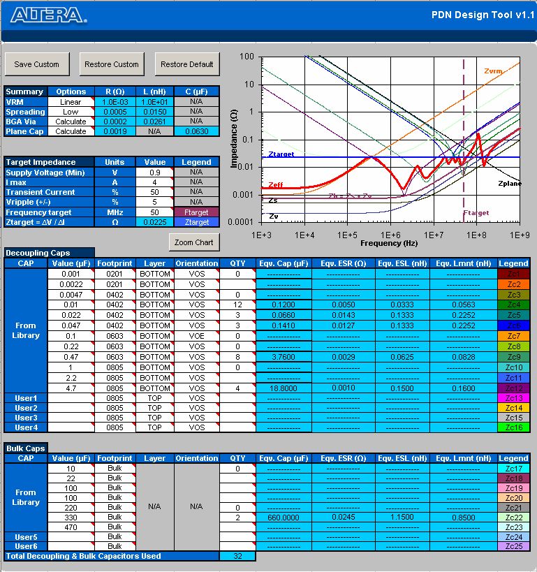
1–2                                                                              Chapter 1: Power Delivery Network (PDN) Tool User Guide
                                                                                                                 Setting Up the PDN Tool

                          Beyond lower frequencies, the VRM impedance is primarily inductive, making it
                          incapable of meeting the transient current requirement. The on-board discrete
                          decoupling capacitors must provide the required low impedance from low to high
                          frequencies, depending on the capacitor intrinsic parasitics (RcN, CcN, LcN) and the
                          capacitor mounting inductance (LmntN). The interplanar capacitance between the
                          power-ground planes typically has lower inductance than the discrete decoupling
                          capacitor network, making it more effective at higher frequencies (tens of MHz). The
                          effectiveness of the decoupling capacitors is limited by the PCB spreading inductance
                          and the ball grid array (BGA) via inductance that a given capacitor encounters with
                          respect to the FPGA. To simplify the circuit topology, the PDN tool models the
                          distributed nature of PCB spreading, BGA inductance, and resistance with a single
                          lumped inductor and resistor.

Figure 1–1. PDN Circuit Topology

                                                                                      Rs        Ls    Rv    Lv

          Rvrm     Lvrm                                                                Spreading       BGR Via
                                                                                        R and L        R and L
                          Lmnt1       Lmnt2         Lmnt3    LmntN

                                                                            Rp

            VRM                                                                                                      Altera FPGA
                           Lc1         Lc2            Lc3     LcN
                                                                            Cp                                          Device
                                                                                      Planar
                          Cc1         Cc2            Cc3      CcN                     R and C

                          Rc1         Rc2            Rc3      RcN

       VRM Model

                                               Decoupling
                                               CAP Model

Setting Up the PDN Tool
                          Figure 1–2 shows the various tabs of the PDN tool spreadsheet.

Figure 1–2. Tabs in the PDN Tool

                          Table 1–1 describes the PDN tool tabs.

Table 1–1. Description of Tabs in PDN Tool (Sheet 1 of 2)
 Tab                               Description
 Release Notes                     This tab provides the legal disclaimers, the revision history of the tool, and the user
                                   agreement.
 Introduction                      This tab shows the schematic representation of the circuit that is modeled as part of the PDN
                                   tool. The tab also provides a brief Quick Start instruction on using the tool.
 Decap Selection                   This tab provides an interface to input the various parameters and observe the resultant
                                   impedance profile. This is the main user interface to the tool.

Power Delivery Network (PDN) Tool User Guide                                                           © March 2009 Altera Corporation
Chapter 1: Power Delivery Network (PDN) Tool User Guide 1–3
Setting Up the PDN Tool
Table 1–1. Description of Tabs in PDN Tool (Sheet 2 of 2)
Tab Description
Library This tab points to various libraries (capacitor, dielectric materials, and so on) that are called
by other tabs. You can change the default values listed as part of these libraries.
BGA Via This tab provides an interface to calculate the BGA mounting inductance based on
design-specific via parameters and the number of vias.
Plane Cap This tab provides an interface to calculate the plane capacitance based on design-specific
parameters.
Cap Mount This tab provides an interface to input design-specific parameters for calculating the
capacitor mounting inductance for two different capacitor orientations (Via on Side [VOS]
and Via on End [VOE]).
X2Y Mount This tab provides an interface to input design-specific parameters for calculating the
capacitor mounting inductance for X2Y type capacitors.
BOM The Bill of Materials (BOM) tab provides a summary of the final capacitor count required to
meet the target impedance.
The PDN tool is designed to provide an accurate estimate on the number and types of
capacitors required to design a robust PDN, regardless of where you are in the design
phase. The accuracy of the results is highly dependent on the user inputs for the
various parameters.
1 You can explore the tool by following the Quick Start instructions listed in the
Introduction tab.
In the pre-layout phase of the design cycle, when no specific information about the
board stackup and board layout is known, you can follow the “Pre-Layout
Instructions” on page 1–3 to explore the solution space when finalizing key design
parameters, such as stackup, plane size, capacitor count, capacitor orientation, and so
on.
If you have finalized the board stackup and have access to board database and layout
information, you can step through the various tabs and enter the required information
to arrive at a very accurate decoupling scheme.
Pre-Layout Instructions
In the pre-layout phase, you can ignore the Plane Cap, Cap Mount, X2Y Mount, and
BGA Via tabs and go directly to the Library tab when you do not have layout
information. Figure 1–3 shows the fields located in the Library tab for entering the
various parameters.
If available, enter the values shown in Figure 1–3 in the Library tab. To use the default
values, go directly to the Decap Selection tab to begin the analysis.
© March 2009 Altera Corporation Power Delivery Network (PDN) Tool User Guide1–4 Chapter 1: Power Delivery Network (PDN) Tool User Guide
Setting Up the PDN Tool
Figure 1–3. Library Tab
Notes to Figure 1–3:
The numbers in Figure 1–3 correspond to the follwing steps 1, 2, 3, 4, 5.
(1) Enter the ESR, ESL, and Lmount values for the capacitors under the Custom field.
(2) Enter the effective BGA via (loop) parasitics for the power supply being decoupled.
(3) Enter the plane capacitance seen by the power/ground plane pair on the board for the power supply under Plane Cap.
(4) Enter the VRM parasitics, if available, under the Custom row.
(5) Enter the effective spreading inductance seen by the decoupling capacitors in the Custom row.
For more information on the Decap Selection tab, refer to “Decap Selection Tab” on
page 1–16.
Power Delivery Network (PDN) Tool User Guide © March 2009 Altera CorporationChapter 1: Power Delivery Network (PDN) Tool User Guide 1–5
Setting Up the PDN Tool
Figure 1–4 shows the various components (VRM, Spreading, BGA Via, and Plane
Cap) of the PDN. In the Decap Selection tab, select the option most applicable for
your design to begin the analysis for a given power supply. In this example, use the
values populated in the Custom field in the Library tab, choose the Custom setting
for the various parameters in the Decap Selection tab.
Figure 1–4. Options for the PDN Components
The following information helps you accurately calculate the ZTARGET for any power
rail:
■ The maximum transient current requirements for all devices in the system that are
powered by the power rail under consideration. You can obtain this information
from the manufacturers of the respective devices.
1 Altera provides the PowerPlay Early Power Estimator (EPE) tool to
estimate power consumption for all its FPGA and CPLD devices. You can
download the EPE tool from the PowerPlay Early Power Estimator
Downloads for your target Altera device. You can also use the Quartus® II
PowerPlay Power Analyzer for an accurate estimation when the design is
implemented.
■ The maximum allowable AC ripple on the power rail as a percentage of the supply
voltage. You can obtain this information from the power supply tolerance
specifications of the devices being supplied by the power rail under consideration.
■ Information regarding the Frequency Target (FTARGET) to which the board PDN
decoupling needs to be effective.
© March 2009 Altera Corporation Power Delivery Network (PDN) Tool User Guide1–6 Chapter 1: Power Delivery Network (PDN) Tool User Guide
Setting Up the PDN Tool
The upper limit of the frequency target for a given supply can be determined from the
plot where the series combination of the plane spreading inductance and the BGA via
inductance (ZSPREAD + ZVIA) profile crosses the ZTARGET profile. Figure 1–5 shows the
upper limit of frequency target calculation.
Figure 1–5. Frequency Target Calculation
Decoupling using PCB capacitors becomes ineffective at high frequency. There is a
cut-off frequency that you must decouple the power supply up to. This frequency
ranges from tens of MHz to higher depending on the parameters, such as parasitic
inductance, OPD capacitors, and ODC, of selected power rail. Altera has new
family-specific PDN tools released that provide a suggested cut-off frequency,
FEFFECTIVE, as the guide line for PCB decoupling.
f For information regarding the availability of the PDN tool that targets your device,
refer to the Altera website at www.altera.com.
You must determine the proper FTARGET in case the information regarding the PCB
decoupling cut-off frequency is not available. You must decouple the power supply
up to this frequency and expect the package and die parasitics to take over the
decoupling for higher frequencies. For most supplies, this frequency is around
80 MHz for any power supply with reasonable ZTARGET. Expect this frequency to be
even lower, in the range of 50 MHz for the core power supply. Expect the device to
take over at a frequency lower than the maximum frequency target that can be
achieved on an optimally designed board (specifically for the Stratix® II GX, Stratix III,
and Stratix IV device families).
After all this information is available, ZTARGET can be calculated as:
Equation 1–1.
%Ripple
VoltageRail • ----------------------
100
Z TARGET = ----------------------------------------------------------
MaxTransientCurrent
Power Delivery Network (PDN) Tool User Guide © March 2009 Altera CorporationChapter 1: Power Delivery Network (PDN) Tool User Guide 1–7
Setting Up the PDN Tool
For example, to reliably decouple a 0.9-volt power rail up to 50 MHz with 5%
AC ripple and a maximum current of 4 A, (assuming 50% of which is transcient
current), ZTARGET can be calculated as:
Equation 1–2.
(0.9)(0.05)
Z TARGET = -------------------------- = 0.0225
4x0.5
Figure 1–6 shows the ZTARGET calculation from the PDN tool.
Figure 1–6. ZTARGET Calculation
To achieve a very low impedance profile (Zeff) below the target impedance (ZTARGET)
up to the desired frequency, the power delivery network relies on the VRM, the
on-board discrete decoupling capacitors, inter-plane capacitance, and a low value of
spreading and mounting inductances.
Figure 1–7 shows one of the capacitor combinations that you can select to ensure that
the effective impedance remains below 0.0225 Ω until the frequency range of interest
(50 MHz). There are many combinations, but the ideal solution is to minimize the
quantity and the type of capacitors required to achieve a flat impedance profile below
the target impedance.
© March 2009 Altera Corporation Power Delivery Network (PDN) Tool User Guide1–8 Chapter 1: Power Delivery Network (PDN) Tool User Guide
Setting Up the PDN Tool
Figure 1–7. Decoupling Example
[
Power Delivery Network (PDN) Tool User Guide © March 2009 Altera CorporationChapter 1: Power Delivery Network (PDN) Tool User Guide 1–9
Setting Up the PDN Tool
Tabs in the PDN Tool
This section describes the various tabs in detail. You can input design-specific
information in the various tabs to arrive at a very accurate PDN profile for a given
power supply.
Library Tab
Figure 1–8 shows the Library tab.
Figure 1–8. Library Tab
This tab is divided into the following sections:
■ Two-Terminal Decoupling Capacitors (High/Mid Frequency)
■ X2Y Decoupling Capacitors (High/Mid Frequency) (High/Mid Frequency)
■ Bulk Capacitors (Mid/Low Frequency)
■ BGA Via and Plane Capacitance
© March 2009 Altera Corporation Power Delivery Network (PDN) Tool User Guide1–10 Chapter 1: Power Delivery Network (PDN) Tool User Guide
Setting Up the PDN Tool
■ VRM Library
■ Spreading R, L Parasitics
■ Dielectric Material Library
You can change each of the default values listed in the respective sections to meet the
specific requirements of your design.
Two-Terminal Decoupling Capacitors
The decoupling capacitors section contains the default ESR and ESL values for the
various two-terminal capacitors in different footprints (0201, 0402, 0603, 0805, and
1206). You also can either modify the default values or enter your own custom values
in the Custom field. If you use a non-two-terminal capacitor, such as an IDC-type
capacitor, you must use the Custom field to enter the capacitor parasitics and the
corresponding mounting inductance.
The decoupling capacitors section also provides the option for the user-defined
capacitors (such as User1, ..., User4). You can define the ESR and ESL parasitics for the
various footprints and enter the corresponding capacitor value in the Decap Selection
tab. Choose the corresponding footprint when defining the capacitor values.
X2Y Decoupling Capacitors (High/Mid Frequency)
The decoupling capacitors section contains the default ESR and ESL values for the
various X2Y capacitors in different footprints (0603, 0805, 1206, and 1210). You also
can replace the default ESR and ESL values with your own custom values.
Bulk Capacitors
The bulk capacitors section contains the commonly used capacitor values for
decoupling the power supply at mid/low frequencies. You can change the default
values to reflect the parameters specific to the design.
BGA Via and Plane Capacitance
The BGA via and plane capacitance section provides an option to directly enter the
values for effective via loop inductance under the BGA and plane capacitance during
the pre-layout phase when no design-specific information is available.
If you have access to design-specific information, you can ignore this section and
enter the design-specific information in the Plane Cap and BGA Via tabs that
calculate the plane capacitance and the BGA via parasitics, respectively.
VRM Library
The VRM section lists the default values for both the linear and switcher regulators.
You can change the VRM parasitics listed under the linear/switcher rows or add the
custom parasitics for the VRM relevant to the design in the Custom field.
Power Delivery Network (PDN) Tool User Guide © March 2009 Altera CorporationChapter 1: Power Delivery Network (PDN) Tool User Guide 1–11
Setting Up the PDN Tool
Spreading R, L Parasitics
The spreading R, L library provides various options for the default effective spreading
inductance values that the decoupling capacitors see with respect to the FPGA based
on the quality of the PDN design.
You can choose a Low value of effective spreading inductance if you have optimally
designed your PDN. Optimum PDN design involves implementing the following
design rules:
■ PCB stackup that provides a wide solid power/ground sandwich for a given
supply with a thin dielectric between the planes. This minimizes the current loop,
which reduces the spreading inductance. The thickness of the dielectric material
between the power/ground pair directly influences the amount of spreading/loop
inductance that a decoupling cap can see with respect to the FPGA.
■ Placing Capacitors closer to the FPGA from an electrical standpoint.
■ Minimizing via perforations in the power/ground sandwich in the current path
from the decoupling caps to the FPGA device.
Due to layout and design constraints, the PDN design might not be optimum; thus,
you can choose either a Medium or High value of spreading R and L. You also can
change the default values or use the Custom field listed in the library specific to the
design.
Dielectric Material Library
The dielectric materials section lists the dielectric constant values for the various
dielectric materials. These values are used in the plane capacitance calculations listed
under the Plane Cap tab. You can change the values listed in this section.
If you change the default values listed in the various sections in the Library tab, you
can save the changes by clicking Save Custom. You can restore the default library by
clicking Restore Default located at the top right corner of the Library page. You also
can restore the saved custom library by clicking Restore Custom.
© March 2009 Altera Corporation Power Delivery Network (PDN) Tool User Guide1–12 Chapter 1: Power Delivery Network (PDN) Tool User Guide
Setting Up the PDN Tool
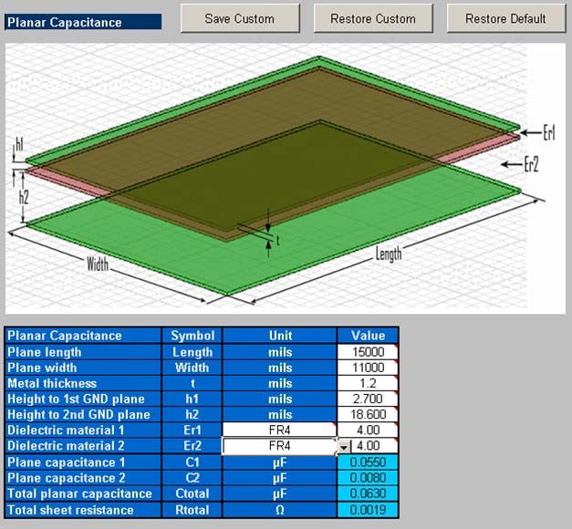
Plane Cap Tab
The Plane Cap tab is used to calculate the distributed plane capacitance in
microfarads (µf) that develops between the power/ground planes with a parallel
plate capacitor equation. Figure 1–9 shows the Plane Cap tab.
Figure 1–9. Plane Cap Tab
You can enter the details specific to this design, for example plane dimensions,
dielectric material, and plane configuration to calculate an accurate capacitance value.
Similar to the Library tab, you can save custom values, restore custom values, and
restore the default settings.
Power Delivery Network (PDN) Tool User Guide © March 2009 Altera CorporationChapter 1: Power Delivery Network (PDN) Tool User Guide 1–13
Setting Up the PDN Tool
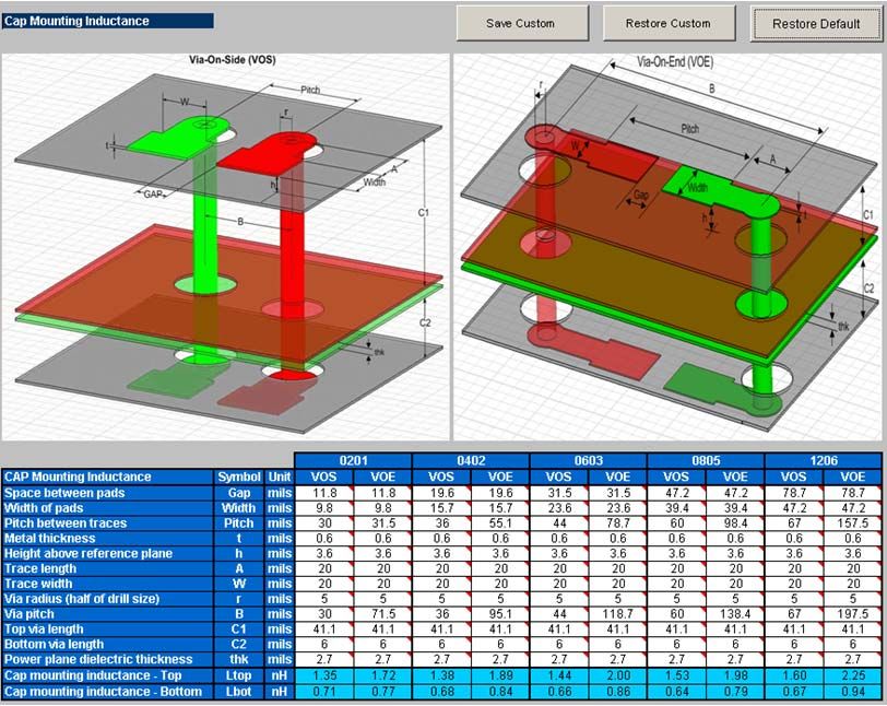
Cap Mount Tab
The Cap Mount tab, shown in Figure 1–10, is used to calculate the capacitor mounting
inductance seen by the decoupling capacitor.
Figure 1–10. Cap Mount Tab
The capacitor mounting calculation is based on the assumption that the decoupling
capacitor is a two-terminal device. The capacitor mounting calculation is applicable
for any two-terminal capacitor with the following footprints: 0201, 0402, 0603, 0805,
1206, and so on. Based on the layout, you can enter all the information and the tool
will provide a mounting inductance for a capacitor mounted on either the top or
bottom layer of the board. Depending on the layout, you can choose between Via on
End or Via on Side to acheive an accurate capacitor mounting inductance value.
If you plan to use a different footprint capacitor other than a regular two-terminal
capacitor or X2Y capacitor for decoupling , you can skip using the Cap Mount tab and
directly enter the capacitor parasitics and capacitor mounting inductance in the
Library tab (under the Custom field in the Decoupling Cap section of the library). As
with the other tabs, you can save the changes made to the tab, restore the changes, and
restore the tab back to the default settings.
© March 2009 Altera Corporation Power Delivery Network (PDN) Tool User Guide1–14 Chapter 1: Power Delivery Network (PDN) Tool User Guide
Setting Up the PDN Tool
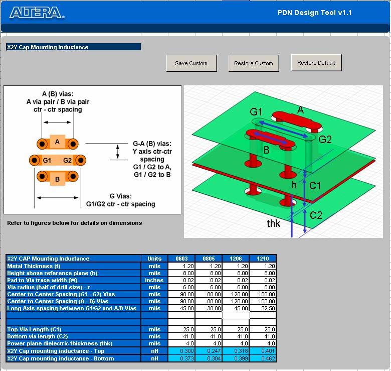
X2Y Mount Tab
The X2Y Mount tab, shown in Figure 1–11, is used to calculate the capacitor mounting
inductance seen by the X2Y decoupling capacitor.
Figure 1–11. X2Y Mount Tab
User inputs in this tab are similar to those in the Cap Mount tab except that the VOE
or VOS options are not required. If you plan to use a different footprint capacitor
other than those available in the tool, you can skip using this tab and directly enter the
capacitor parasitics and capacitor mounting inductance in the Library tab (replacing
the preset value with your own data in the X2Y Decoupling Cap section). As with the
other tabs, you have can save the changes made to the tab, restore the changes, and
restore the tab back to the default settings.
Power Delivery Network (PDN) Tool User Guide © March 2009 Altera CorporationChapter 1: Power Delivery Network (PDN) Tool User Guide 1–15
Setting Up the PDN Tool
BGA Via Tab
The BGA Via tab is used to calculate the vertical via loop inductance under the BGA
pin field. Figure 1–12 shows teh BGA Via tab.
Figure 1–12. BGA Via Tab
This tab takes the layout-specific information, such as the via drill diameter, via
length, via pitch, and the number of power/ground via pairs under the BGA for an
effective via loop inductance and resistance value.
© March 2009 Altera Corporation Power Delivery Network (PDN) Tool User Guide1–16 Chapter 1: Power Delivery Network (PDN) Tool User Guide
Setting Up the PDN Tool
Decap Selection Tab
The Decap Selection tab, shown in Figure 1–13, is the main tab where you perform
the analysis.
Figure 1–13. Decap Selection Tab
[
In the Decap Selection window, you can either enable or disable the following
components of the PDN:
■ VRM
■ Spreading Parasitics
■ BGA Via
■ Plane Capacitance
VRM
You can choose either to Ignore or include the VRM parasitics for a Linear, Switcher,
or Custom VRM parasitics.
Power Delivery Network (PDN) Tool User Guide © March 2009 Altera CorporationChapter 1: Power Delivery Network (PDN) Tool User Guide 1–17
Setting Up the PDN Tool
Spreading Parasitics
Based on the design, you can select either a Low, Medium, High, or Custom value for
the effective spreading R, L values that the decoupling capacitors see with respect to
the FPGA. You can ignore the spreading inductance. Ignoring the spreading
inductance leads to an optimistic result and is not an accurate representation of the
impedance profile that the FPGA encounters.
The Ignore option helps you understand that the spreading inductance in
combination with the BGA via inductance is the limiting factor from a PCB
perspective to decouple the FPGA at high frequencies. Be careful when choosing the
Ignore option while estimating a final capacitor count.
BGA Via
Based on the design, you can either Ignore the BGA via component or Calculate the
effective via inductance based on the layout. If you are in the middle of layout, you
can directly enter the effective loop R, L via parasitics in the Library tab and choose
the Custom setting under BGA Via to include the via parasitics.
Plane Capacitance
Based on the design, you can either Ignore the interplanar capacitance between the
power and ground plane, or Calculate the plane capacitance based on the layout. If
you are in the middle of layout, you can directly enter the plane capacitance in the
Library tab and choose the Custom setting under Plane Cap to include the plane
capacitance parasitics.
The next section in the Decap Selection tab deals with target impedance calculation
that was described earlier in the user guide.
The final section in the Decap Selection tab provides the ability to select the various
high/mid frequency decoupling capacitors based on footprint, layer, and orientation
to meet the target impedance you can choose X2Y type of capacitors in the Footprint
column besides two-terminal capacitors. The capacitance value for the X2Y capacitor
may be different from that of the two-terminal capacitor. A warning message of
"Wrong Footprint" is displayed if you choose a wrong combination of capacitance and
footprint. You can define custom capacitor values (such as User1, ..., User4) needed
for high/mid frequency decoupling specific to the design. However, you cannot
change the capacitor parasitics (ESR and ESL) in this tab. This can only be done in the
Library tab.
You can change the parasitics of the bulk decoupling capacitors in the Library tab and
define the mounting inductance specific to the design. You also can define custom
capacitor values (such as User5, User6) for low/mid frequency decoupling specific to
the design.
As provided in other tabs, you can save and restore the final capacitor count and other
settings for a specific set of assumptions. You can also revert back to default settings.
© March 2009 Altera Corporation Power Delivery Network (PDN) Tool User Guide1–18 Chapter 1: Power Delivery Network (PDN) Tool User Guide
Setting Up the PDN Tool
BOM Tab
Figure 1–14 shows the BOM tab.
Figure 1–14. BOM Tab
When the analysis is done, you can print the final Zeff profile and capacitor count to
achieve the profile by clicking Print BOM on the top right corner. It defaults to the
default printer assigned on the File menu under Print. You can also export the data as
an .xls file by clicking Export Data.
Power Delivery Network (PDN) Tool User Guide © March 2009 Altera CorporationChapter 1: Power Delivery Network (PDN) Tool User Guide 1–19
Summary
Summary
This user guide provides a brief overview of the various tabs in the PDN tool. You can
quickly and accurately design a robust PDN by calculating an optimum number of
capacitors that meet the target impedance requirements for a given power supply.
© March 2009 Altera Corporation Power Delivery Network (PDN) Tool User Guide1–20 Chapter 1: Power Delivery Network (PDN) Tool User Guide
Summary
Power Delivery Network (PDN) Tool User Guide © March 2009 Altera CorporationAdditional Information
Document Revision History
The table below displays the revision history for the chapters in this User Guide.
Document
Date Version Changes Made
March 2009 2.0 ■ Added X2Y Mount information.
■ Added X2Y Decoupling Capacitors information.
■ Added PDN Decoupling Methodology Review section.
■ Updated PDN Circuit Topology section.
■ Updated Pre-Layout Instructions section.
■ Updated graphics.
■ Converted to the 8.5 × 11 template.
April 2008 1.0 Initial release.
How to Contact Altera
For the most up-to-date information about Altera® products, refer to the following
table.
Contact
Contact (1) Method Address
Technical support Website www.altera.com/support
Technical training Website www.altera.com/training
Email custrain@altera.com
Product literature Website www.altera.com/literature
Non-technical support (General) Email nacomp@altera.com
Non-technical support (Software Email authorization@altera.com
Licensing)
Note to table:
(1) You can also contact your local Altera sales office or sales representative.
© March 2009 Altera Corporation Power Delivery Network (PDN) Tool User GuideInfo–2
Typographic Conventions
Typographic Conventions
This document uses the typographic conventions shown below.
Visual Cue Meaning
Bold Type with Initial Command names, dialog box titles, checkbox options, and dialog box options are shown in
Capital Letters bold, initial capital letters. Example: Save As dialog box.
bold type External timing parameters, directory names, project names, disk drive names, file names, file
name extensions, and software utility names are shown in bold type. Examples: fMAX,
\qdesigns directory, d: drive, chiptrip.gdf file.
Italic Type with Initial Document titles are shown in italic type with initial capital letters. Example: AN 75: High-Speed
Capital Letters Board Design.
Italic type Internal timing parameters and variables are shown in italic type.
Examples: tPIA, n + 1.
Variable names are enclosed in angle brackets (< >) and shown in italic type. Example: , .pof file.
Initial Capital Letters Keyboard keys and menu names are shown with initial capital letters. Examples: Delete key, the
Options menu.
“Subheading Title” References to sections within a document and titles of on-line help topics are shown in
quotation marks. Example: “Typographic Conventions.”
Courier type Signal and port names are shown in lowercase Courier type. Examples: data1, tdi, input.
Active-low signals are denoted by suffix n, e.g., resetn.
Anything that must be typed exactly as it appears is shown in Courier type. For example:
c:\qdesigns\tutorial\chiptrip.gdf. Also, sections of an actual file, such as a Report
File, references to parts of files (e.g., the AHDL keyword SUBDESIGN), as well as logic function
names (e.g., TRI) are shown in Courier.
1., 2., 3., and Numbered steps are used in a list of items when the sequence of the items is important, such
a., b., c., etc. as the steps listed in a procedure.
■ ● • Bullets are used in a list of items when the sequence of the items is not important.
v The checkmark indicates a procedure that consists of one step only.
1 The hand points to information that requires special attention.
A caution calls attention to a condition or possible situation that can damage or destroy the
c
product or the user’s work.
A warning calls attention to a condition or possible situation that can cause injury to the user.
w
r The angled arrow indicates you should press the Enter key.
f The feet direct you to more information on a particular topic.
Power Delivery Network (PDN) Tool User Guide © March 2009 Altera CorporationYou can also read