Clocking Wizard v6.0 LogiCORE IP Product Guide - Vivado Design Suite - Xilinx
←
→
Page content transcription
If your browser does not render page correctly, please read the page content below
Clocking Wizard v6.0

LogiCORE IP Product Guide

Vivado Design Suite
PG065 February 5, 2020
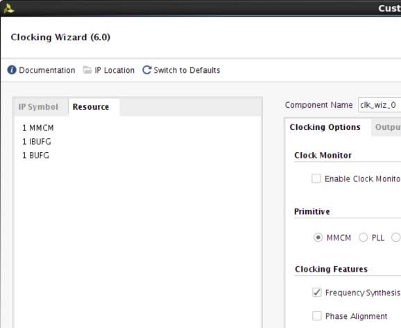
Table of Contents
       IP Facts

       Chapter 1: Overview
          About the Core . . . . . . . . . . . . . . . . . . . . . . . . . . . . . . . . . . . . . . . . . . . . . . . . . . . . . . . . . . . . . . . . . . . .       5
          Recommended Design Experience . . . . . . . . . . . . . . . . . . . . . . . . . . . . . . . . . . . . . . . . . . . . . . . . . . . .                        5
          Feature Summary. . . . . . . . . . . . . . . . . . . . . . . . . . . . . . . . . . . . . . . . . . . . . . . . . . . . . . . . . . . . . . . . . .           6
          Applications . . . . . . . . . . . . . . . . . . . . . . . . . . . . . . . . . . . . . . . . . . . . . . . . . . . . . . . . . . . . . . . . . . . . . .     7
          Licensing and Ordering . . . . . . . . . . . . . . . . . . . . . . . . . . . . . . . . . . . . . . . . . . . . . . . . . . . . . . . . . . . . .             7

       Chapter 2: Product Specification
          Performance. . . . . . . . . . . . . . . . . . . . . . . . . . . . . . . . . . . . . . . . . . . . . . . . . . . . . . . . . . . . . . . . . . . . . . 8
          Resource Utilization. . . . . . . . . . . . . . . . . . . . . . . . . . . . . . . . . . . . . . . . . . . . . . . . . . . . . . . . . . . . . . . . 9
          Port Descriptions . . . . . . . . . . . . . . . . . . . . . . . . . . . . . . . . . . . . . . . . . . . . . . . . . . . . . . . . . . . . . . . . . 10
          Register Space . . . . . . . . . . . . . . . . . . . . . . . . . . . . . . . . . . . . . . . . . . . . . . . . . . . . . . . . . . . . . . . . . . . 14

       Chapter 3: Designing with the Core
          General Design Guidelines . . . . . . . . . . . . . . . . . . . . . . . . . . . . . . . . . . . . . . . . . . . . . . . . . . . . . . . . .                  23
          Clocking. . . . . . . . . . . . . . . . . . . . . . . . . . . . . . . . . . . . . . . . . . . . . . . . . . . . . . . . . . . . . . . . . . . . . . . . .    23
          Resets . . . . . . . . . . . . . . . . . . . . . . . . . . . . . . . . . . . . . . . . . . . . . . . . . . . . . . . . . . . . . . . . . . . . . . . . . .   23
          Functional Overview . . . . . . . . . . . . . . . . . . . . . . . . . . . . . . . . . . . . . . . . . . . . . . . . . . . . . . . . . . . . . .              24
          Core Architecture. . . . . . . . . . . . . . . . . . . . . . . . . . . . . . . . . . . . . . . . . . . . . . . . . . . . . . . . . . . . . . . . .           30

       Chapter 4: Design Flow Steps
          Customizing and Generating the Core . . . . . . . . . . . . . . . . . . . . . . . . . . . . . . . . . . . . . . . . . . . . . . . .                          32
          Constraining the Core . . . . . . . . . . . . . . . . . . . . . . . . . . . . . . . . . . . . . . . . . . . . . . . . . . . . . . . . . . . . .              58
          Simulation . . . . . . . . . . . . . . . . . . . . . . . . . . . . . . . . . . . . . . . . . . . . . . . . . . . . . . . . . . . . . . . . . . . . . .       59
          Synthesis and Implementation . . . . . . . . . . . . . . . . . . . . . . . . . . . . . . . . . . . . . . . . . . . . . . . . . . . . . .                     60

       Chapter 5: Example Design
          Directory and File Contents. . . . . . . . . . . . . . . . . . . . . . . . . . . . . . . . . . . . . . . . . . . . . . . . . . . . . . . . . 61
          Example Design . . . . . . . . . . . . . . . . . . . . . . . . . . . . . . . . . . . . . . . . . . . . . . . . . . . . . . . . . . . . . . . . . . 61

Clocking Wizard v6.0                                                                                                               Send Feedback
                                                                                                                                                                       2
PG065 February 5, 2020                                             www.xilinx.com
Chapter 6: Test Bench
Appendix A: Verification, Compliance, and Interoperability
Simulation . . . . . . . . . . . . . . . . . . . . . . . . . . . . . . . . . . . . . . . . . . . . . . . . . . . . . . . . . . . . . . . . . . . . . . 63
Hardware Testing. . . . . . . . . . . . . . . . . . . . . . . . . . . . . . . . . . . . . . . . . . . . . . . . . . . . . . . . . . . . . . . . . 63
Appendix B: Upgrading
Migrating to the Vivado Design Suite. . . . . . . . . . . . . . . . . . . . . . . . . . . . . . . . . . . . . . . . . . . . . . . . . 64
Differences between the Clocking Wizard and the Legacy DCM and PLL Wizards . . . . . . . . . . . . . 64
Upgrading in the Vivado Design Suite . . . . . . . . . . . . . . . . . . . . . . . . . . . . . . . . . . . . . . . . . . . . . . . . 65
Appendix C: Debugging
Finding Help on Xilinx.com . . . . . . . . . . . . . . . . . . . . . . . . . . . . . . . . . . . . . . . . . . . . . . . . . . . . . . . . . 67
Debug Tools . . . . . . . . . . . . . . . . . . . . . . . . . . . . . . . . . . . . . . . . . . . . . . . . . . . . . . . . . . . . . . . . . . . . . 68
Hardware Debug . . . . . . . . . . . . . . . . . . . . . . . . . . . . . . . . . . . . . . . . . . . . . . . . . . . . . . . . . . . . . . . . . 69
Appendix D: Additional Resources and Legal Notices
Xilinx Resources . . . . . . . . . . . . . . . . . . . . . . . . . . . . . . . . . . . . . . . . . . . . . . . . . . . . . . . . . . . . . . . . . . 71
Documentation Navigator and Design Hubs . . . . . . . . . . . . . . . . . . . . . . . . . . . . . . . . . . . . . . . . . . . 71
References . . . . . . . . . . . . . . . . . . . . . . . . . . . . . . . . . . . . . . . . . . . . . . . . . . . . . . . . . . . . . . . . . . . . . . 72
Revision History . . . . . . . . . . . . . . . . . . . . . . . . . . . . . . . . . . . . . . . . . . . . . . . . . . . . . . . . . . . . . . . . . . 73
Please Read: Important Legal Notices . . . . . . . . . . . . . . . . . . . . . . . . . . . . . . . . . . . . . . . . . . . . . . . . 74
Clocking Wizard v6.0 Send Feedback
3
PG065 February 5, 2020 www.xilinx.comIP Facts
Introduction LogiCORE IP Facts Table
Core Specifics
The Clocking Wizard LogiCORE™ IP simplifies
Supported Device UltraScale+™ families, UltraScale™ families,
the creation of HDL source code wrappers for Family(1) Zynq®-7000 SoC, 7 Series
clock circuits customized to your clocking Supported User
AXI4-Lite
requirements. The Wizard guides you in setting Interfaces
the appropriate attributes for your clocking Resources Performance and Resource Utilization web page.
primitive, and allows you to override any Special Features PLL(E2/E3/E4), MMCM(E2/E3/E4),
wizard-calculated parameter. In addition to Spread Spectrum Clocking
providing an HDL wrapper for implementing Provided with Core
the desired clocking circuit, the Clocking
Design Files Verilog(2)
Wizard also delivers a timing parameter
Example Design Verilog
summary generated by the Xilinx® timing tools
for the circuit. Test Bench Verilog(2)
Constraints File .xdc (Xilinx Design Constraints)
For supported simulators, see the Xilinx
Simulation Model
Features Instantiation
Design Tools: Release Notes Guide.
Verilog and VHDL Wrapper
Template
• The selection of mixed-mode clock Supported
manager (MMCM) and phase-locked loop S/W Driver
Not Applicable
(PLL) primitives. Integrated design
Tested Design Flows
environment (IDE) options are enabled for
the supported features for the primitives. Design Entry Tools Vivado® Design Suite
Mentor Graphics Questa Advanced
• The Safe Clock Startup feature enables a Simulation
Simulator, Vivado Simulator
stable and valid clock at the output.
Synthesis Tools Synplify PRO E-2012.03, Vivado Synthesis
Enabling the Sequencing feature provides
sequenced output clocks. Support
• Accepts up to two input clocks and up to Release Notes and
Master Answer Record: 54102
Known Issues
seven output clocks per clock network.
All Vivado IP
• Provides an AXI4-Lite interface for Change Logs
Master Vivado IP Change Logs: 72775
dynamically reconfiguring the clocking Xilinx Support web page
primitives for Multiply, Divide, Phase Shift/
Offset, or Duty Cycle. Notes:
1. For a complete listing of supported devices, see the Vivado IP
• Automatically configures a clocking Catalog.
primitive based on the selected clocking 2. The top RTL design file is delivered in Verilog and the
sub-modules can still be in VHDL or Verilog.
features.
3. A standalone C example can be found in the Vitis directory
• Automatically calculates the (/data/embeddedsw/XilinxProcessorIPLib/
drivers/clk_wiz_vx_x). Linux OS and driver support information
voltage-controlled oscillator (VCO)
is available from the Xilinx Wiki page. Common clock Linux
frequency for primitives with an oscillator, driver information for Zynq UltraScale+ MPSoCs is available from
and provides multiply and divide values the Common Clock Framework Wiki page.
based on input and output frequency 4. For the supported versions of third-party tools, see the
Xilinx Design Tools: Release Notes Guide.
requirements.
Clocking Wizard v6.0 Send Feedback 4
PG065 February 5, 2020 www.xilinx.com Product SpecificationChapter 1
Overview
This chapter introduces the Clocking Wizard core and provides related information,
including recommended design experience, additional resources, technical support, and
ways of submitting feedback to Xilinx. The Clocking Wizard core generates source register
transfer level (RTL) code to implement a clocking network matched to your requirements.
Both Verilog and VHDL design environments are supported.
About the Core
The Clocking Wizard is a Xilinx ® IP core that can be generated using the Xilinx Vivado
design tools, included with the latest Vivado release in the Xilinx Download Center.
The core is licensed under the terms of the Xilinx End User License, and no FLEX license key
is required.
Recommended Design Experience
The Clocking Wizard is designed for users with any level of experience. Using the Wizard
automates the process of creating your clocking network and is highly recommended. The
Wizard guides you to the proper primitive configuration and allows advanced users to
override and manually set any attribute. Although the Clocking Wizard provides a fully
verified clocking network, understanding the Xilinx clocking primitives aids you in making
design trade-off decisions.
Clocking Wizard v6.0 Send Feedback
5
PG065 February 5, 2020 www.xilinx.comChapter 1: Overview
Feature Summary
The clocking options are listed below:
• Frequency Synthesis allows output clocks to have different frequencies from the active
input clock.
• Spread Spectrum provides modulated output clocks, which reduces the spectral
density of the electromagnetic interference (EMI) generated by electronic devices. This
feature is available for the MMCM(E2/E3/E4)_ADV primitive only. UNISIM simulation
support for this feature is not currently available.
• Phase Alignment allows the output clock to be phase locked to a reference, such as
the input clock pin for a device.
• Minimize Power allows you to minimize the amount of power needed for the primitive.
This is at the possible expense of frequency, phase offset, or duty cycle accuracy.
• Dynamic Phase Shift allows you to change the phase relationship on the output
clocks.
• Dynamic Reconfiguration allows you to change the programming of the primitive
after device configuration. When this option is chosen, the AXI4-Lite interface is
selected by default for reconfiguring the clocking primitive.
• Balanced. Selecting Balanced results in the software choosing the correct bandwidth
for jitter optimization.
• Minimize Output Jitter. This feature minimizes the jitter on the output clocks, but at
the expense of power and possibly output clock phase error. This feature is not
available with the Maximize input jitter filtering feature.
• Maximize Input Jitter filtering allows for larger input jitter on the input clocks, but
can negatively impact the jitter on the output clocks. This feature is not available with
the Minimize output jitter feature.
• Safe Clock Startup and Sequencing can be used to get a stable and valid clock at the
output. It also enables clocks in a particular sequence order as specified in the
configuration.
• Clock Monitor helps you to monitor the clock inputs to the Clocking Wizard. It can
monitor up to four clocks. You can monitor if the input frequency is out of range of the
expected frequency, and detect clock stop and glitches in the clock.
• Auto Primitive instantiates the appropriate clocking primitive for your requirements.
You do not need know the specification of the MMCM or PLL to judge which primitive
fits into your requirements; the Wizard does this for you. This feature is available for
UltraScale™ and UltraScale+™ devices only.
Clocking Wizard v6.0 Send Feedback
6
PG065 February 5, 2020 www.xilinx.comChapter 1: Overview
Applications
• The creation of clock networks with the required frequency, phase, and duty cycle, with
reduced jitter.
• Electromagnetic interference reduction in electronic devices using the Spread Spectrum
feature.
Licensing and Ordering
This Xilinx LogiCORE™ IP module is provided at no additional cost with the Xilinx Vivado®
Design Suite under the terms of the Xilinx End User License.
Information about other Xilinx LogiCORE IP modules is available at the Xilinx Intellectual
Property page. For information about pricing and availability of other Xilinx LogiCORE IP
modules and tools, contact your local Xilinx sales representative.
Clocking Wizard v6.0 Send Feedback
7
PG065 February 5, 2020 www.xilinx.comChapter 2
Product Specification
Clocking Wizard helps create the clocking circuit for the required output clock frequency,
phase, and duty cycle using a mixed-mode clock manager (MMCM)(E2/E3/E4) or
phase-locked loop (PLL)(E2/E3/E4) primitive. It also helps verify the output generated clock
frequency in simulation, providing a synthesizable example design which can be tested on
the hardware. It also supports the Spread Spectrum feature, which is helpful in reducing
electromagnetic interference. Figure 2-1 shows a block diagram of the Clocking Wizard.
X-Ref Target - Figure 2-1
Demonstration Test Bench
Example Design
Provided Clocking Network
Frequency
Optional Feedback Check
Optional Optional
Clock Input Configured Output Counter High
Generators Bufs Clocking Bufs
Clocks Clocks Array Bits
Primitive
X12950-022219
Figure 2-1: Clocking Wizard Block Diagram
Performance
Maximum Frequencies
For the maximum frequencies of the MMCM and PLL, refer to the following device data
sheets:
• Virtex-7 T and XT FPGAs Data Sheet (DS183) [Ref 10]
• Kintex-7 FPGAs Data Sheet (DS182) [Ref 11]
• Kintex UltraScale FPGAs Data Sheet (DS892) [Ref 12]
Clocking Wizard v6.0 Send Feedback
8
PG065 February 5, 2020 www.xilinx.comChapter 2: Product Specification
• Virtex UltraScale FPGAs Data Sheet (DS893) [Ref 13]
• Zynq UltraScale+ MPSoC Data Sheet (DS925) [Ref 14]
• Kintex UltraScale+ FPGAs Data Sheet (DS922) [Ref 15]
• Virtex UltraScale FPGAs Data Sheet (DS893) [Ref 16]
Power
• The Minimize Power feature minimizes the amount of power needed for the primitive at
the possible expense of frequency, phase offset, or duty cycle accuracy.
• When asserted, the power down input pin places the clocking primitive in a low power
state, which stops the output clocks.
Resource Utilization
Resource utilization is available in the Clocking Wizard IDE by clicking on the Resource tab.
This does not include AXI4-Lite resources when Dynamic Reconfiguration is enabled.
X-Ref Target - Figure 2-2
Figure 2-2: Resource Tab
Clocking Wizard v6.0 Send Feedback
9
PG065 February 5, 2020 www.xilinx.comChapter 2: Product Specification
Port Descriptions
Table 2-1 describes the input and output ports provided from the clocking network. All
ports are optional, with the exception being that at least one input and one output clock are
required. The options selected determine which ports are actually available to be
configured. For example, when Dynamic Reconfiguration is selected, these ports are
exposed. Any port that is not exposed is appropriately tied off or connected to a signal
labeled unused in the delivered source code.
Table 2-1: Clocking Wizard I/O
Port (5) I/O Description
Input Clock Ports(1)
clk_in1 I Clock in 1 : Single-ended primary input clock port. Available
when single-ended primary clock source is selected.
clk_in1_p I Clock in 1 Positive and Negative: Differential primary input
clock port pair. Available when a differential primary clock
clk_in1_n source is selected.
clk_in2 (2) I Clock in 2: Single-ended secondary input clock port. Available
when a single-ended secondary clock source is selected.
clk_in2_p (2) I Clock in 2 Positive and Negative: Differential secondary input
(2) clock port pair. Available when a differential secondary clock
clk_in2_n source is selected.
clk_in_sel(2) I Clock in Select: When 1, selects the primary input clock; when
0, the secondary input clock is selected. Available when two
input clocks are specified.
clkfb_in I Clock Feedback in: Single-ended feedback in port of the
clocking primitive. Available when user-controlled on-chip,
user controller-off chip, or automatic control off-chip feedback
option is selected.
clkfb_in_p I Clock Feedback in: Positive and Negative: Differential feedback
in port of the clocking primitive. Available when the automatic
clkfb_in_n control off-chip feedback and differential feedback option is
selected.
Output Clock Ports
clk_out1 O Clock Out 1: Output clock of the clocking network. clk_out1 is
not optional.
clk_out1_ce I Clock Enable: Clock enable pin of the output buffer. Available
when BUFGCE or BUFHCE or BUFR or BUFGCE_DIV buffers are
used as output clock drivers.
clk_out1_clr I Counter reset for divided clock output: Available when BUFR or
BUFGCE_DIV buffer is used as output clock driver.
Clocking Wizard v6.0 Send Feedback
10
PG065 February 5, 2020 www.xilinx.comChapter 2: Product Specification
Table 2-1: Clocking Wizard I/O (Cont’d)
Port (5) I/O Description
clk_out2_n (3) O Clock Out 2 - n: Optional output clocks of the clocking network
that are user specified. For an MMCM, up to seven are
available. For UltraScale PLLE3, up to two clocks are available
and for 7 series/Zynq-7000PLLE2, up to six clocks are available.
clk_out[2-n]_ce (3) I Clock Enable: Clock enable pin of the output buffer. Available
when BUFGCE or BUFHCE or BUFR or BUFGCE_DIV buffers are
used as output clock drivers.
clk_out[2-n]_clr(3) I Counter reset for divided clock output: Available when the
BUFR buffer is used as output clock driver.
clkfb_out O Clock Feedback Out: Single-ended feedback port of the
clocking primitive. Available when the user-controlled
feedback or automatic control off chip with single-ended
feedback option is selected.
clkfb_out_p O Clock Feedback Out: Positive and Negative: Differential
feedback output port of the clocking primitive. Available when
clkfb_out_n O the user-controlled off-chip feedback and differential
feedback option is selected.
Dynamic Reconfiguration Ports
daddr[6:0] I Dynamic Reconfiguration Address: Address port for use in
dynamic reconfiguration; active when den is asserted.
dclk I Dynamic Reconfiguration Clock: Clock port for use in dynamic
reconfiguration.
den I Dynamic Reconfiguration Enable: Starts a dynamic
reconfiguration transaction. Refer to DRP protocol details for
more information.
di[15:0] I Dynamic Reconfiguration Data in: Input data for a dynamic
reconfiguration write transaction; active when den is asserted.
do[15:0] O Dynamic Reconfiguration Data Out: Output data for a dynamic
reconfiguration read transaction; active when drdy is asserted.
drdy O Dynamic Reconfiguration Ready: Completes a dynamic
reconfiguration transaction.
dwe I Dynamic Reconfiguration Write Enable: When asserted,
indicates that the dynamic reconfiguration transaction is a
write; active when den is asserted.
Dynamic Phase Shift Ports(2)
psclk I Dynamic Phase Shift Clock: Clock for use in dynamic phase
shifting.
psen I Dynamic Phase Shift Enable: Starts a dynamic phase shift
transaction.
psincdec I Dynamic Phase Shift increment/decrement: When 1,
increments the phase shift of the output clock, when 0,
decrements the phase shift.
Clocking Wizard v6.0 Send Feedback
11
PG065 February 5, 2020 www.xilinx.comChapter 2: Product Specification
Table 2-1: Clocking Wizard I/O (Cont’d)
Port (5) I/O Description
psdone O Dynamic Phase Shift Done: Completes a dynamic phase shift
transaction.
Status and Control Ports(4)
reset/resetn I Reset (active-High)/Resetn (active-Low): When asserted,
asynchronously clears the internal state of the primitive, and
causes the primitive to re-initiate the locking sequence when
released.
power_down I Power Down: When asserted, places the clocking primitive into
a low power state, which stops the output clocks.
input_clk_ stopped O Input Clock Stopped: When asserted, indicates that the
selected input clock is no longer toggling.
locked O Locked: When asserted, indicates that the output clocks are
stable and usable by downstream circuitry.
cddcreq (6) Clock Divide Dynamic Change (CDDC) request. This is asserted
I after last DRP request is performed, and then deasserted after
the last DRDY.
cddcdone (6) Clock Divide Dynamic Change (CDDC) done. When output
O
counters are updated, this signal is asserted.
s_axi_aclk I AXI Clock.
s_axi_aresetn I AXI Reset, active-Low.
s_axi_awaddr[10:0] AXI Write address. The write address bus gives the address of
I
the write transaction.
s_axi_awvalid Write address valid. This signal indicates that a valid write
I
address and control information are available.
s_axi_awready Write address ready. This signal indicates that the slave is
O
ready to accept an address and associated control signals.
s_axi_wdata[31:0] I Write data.
s_axi_wstb[3:0] Write strobes. This signal indicates which byte lanes to update
I
in memory.
s_axi_wvalid Write valid. This signal indicates that valid write data and
I
strobes are available.
s_axi_wready Write ready. This signal indicates that the slave can accept the
O
write data.
s_axi_bresp[1:0] Write response. This signal indicates the status of the write
transaction
O 00 = OKAY (normal response)
10 = SLVERR (error condition)
11 = DECERR (not issued by core)
s_axi_bvalid Write response valid. This signal indicates that a valid write
O
response is available.
Clocking Wizard v6.0 Send Feedback
12
PG065 February 5, 2020 www.xilinx.comChapter 2: Product Specification
Table 2-1: Clocking Wizard I/O (Cont’d)
Port (5) I/O Description
s_axi_bready Response ready. This signal indicates that the master can
I
accept the response information.
s_axi_araddr[10:0] Read address. The read address bus gives the address of a read
I
transaction.
s_axi_arvalid Read address valid. This signal indicates, when High, that the
read address and control information is valid and remains
I
stable until the address acknowledgment signal, s_axi_arready,
is High.
s_axi_arready Read address ready. This signal indicates that the slave is ready
O
to accept an address and associated control signals.
s_axi_rdata[31:0] O Read data.
s_axi_rresp[1:0] Read response. This signal indicates the status of the read
transfer.
O 00 = OKAY (normal response)
10 = SLVERR (error condition)
11 = DECERR (not issued by core)
s_axi_rvalid Read valid. This signal indicates that the required read data is
O
available and the read transfer can complete.
s_axi_rready Read ready. This signal indicates that the master can accept the
I
read data and response information.
s_axis_aclk The global clock signal. All streaming signals from Read
I interface of the FIFO are sampled on the rising edge of
s_axis_aclk.
Clock Monitor Ports (7)
ref_clk This is the input reference clock used to monitor the user
I
clocks. It is considered to be stable and error free.
user_clk0 User clock 0. This port is disabled when the ENABLE_PLL/
I
MMCM0 checkbox is enabled in the Vivado IDE.
user_clk1 User clock 1. This port is disabled when the ENABLE_PLL1/
I
MMCM1 checkbox is enabled in the Vivado IDE.
user_clk2 I User input clock 2 to monitor.
user_clk3 I User input clock 3 to monitor.
clk_stop[3:0] The bits for this port are High when clock is stopped on the
respective user clock.
Bit 0 - User clock 0
O
Bit 1 - User clock 1
Bit 2 - User clock 2
Bit 3 - User clock 3
Clocking Wizard v6.0 Send Feedback
13
PG065 February 5, 2020 www.xilinx.comChapter 2: Product Specification
Table 2-1: Clocking Wizard I/O (Cont’d)
Port (5) I/O Description
clk_OOR[3:0] The bits for this port are High when input clock frequency is
out of range than expected.
Bit 0 - User clock 0
O
Bit 1 - User clock 1
Bit 2 - User clock 2
Bit 3 - User clock 3
clk_glitch[3:0] The bits for this port are High where there is a glitch in the
input clock.
Bit 0 - User clock 0
O
Bit 1 - User clock 1
Bit 2 - User clock 2
Bit 3 - User clock 3
interrupt O This port gives the interrupts of the clock monitor feature.
Notes:
1. At least one input clock is required; any design has at least a clk_in1 or a clk_in1_p/clk_in1_n port.
2. Not available when primitive chosen is UltraScale PLL or Spread Spectrum is selected for MMCM.
3. The clk_out3 and clk_out4 ports are not available when Spread Spectrum is selected.
4. Exposure of every status and control port is individually selectable.
5. This version of Clocking Wizard supports naming of ports as per requirements. The list mentioned in Table 2-1 is the default
port list.
6. Ports used for dynamic change of output counter without reset. Available only in MMCME3 primitive.
7. These ports are available when the Clock Monitor feature is enabled.
Register Space
Table 2-2 shows the set of registers applicable when the Dynamic Reconfiguration mode is
selected. All registers are accessed as 32-bit.
Clocking Wizard v6.0 Send Feedback
14
PG065 February 5, 2020 www.xilinx.comChapter 2: Product Specification
Table 2-2: Clock Configuration Registers
Base Address + Reset
Offset Register Value Access Description
Name Type
(hex) (hex)
C_BASEADDR + Software Reset Register (SRR) N/A W (1) Software Reset Register
0x00 To activate software reset, the
value 0x0000_000A must be
written to the register. Any other
access, read or write, has
undefined results.
C_BASEADDR + Status Register (SR) 0x00000000 R Status Register
0x04 Bit[0] = Locked
When 1 MMCM/PLL is Locked
and ready for reconfiguration.
The status of this bit is 0 during
reconfiguration.
C_BASEADDR Clock Monitor Error Status Register 0x00000000 R This register gives the error
+0x08 status bits of the clock monitor
feature.
C_BASEADDR Interrupt Status 0x00000000 R/W Interrupt Status for Clock Stop,
+0x0C Clock Overrun, and Clock
Underrun. These bits are gated by
Interrupt enable bits. Interrupts
corresponding to the enabled
bits in Interrupt enable register
would be updated in this register.
C_BASEADDR Interrupt Enable 0x00000000 R/W Interrupt Enable for Clock Stop,
+0x10 Clock Overrun, and Clock
Underrun bits in the Interrupt
status register.
Clocking Wizard v6.0 Send Feedback
15
PG065 February 5, 2020 www.xilinx.comChapter 2: Product Specification
Table 2-2: Clock Configuration Registers (Cont’d)
Base Address + Register Reset Access
Offset Value Description
(hex) Name (hex) Type
Dynamic Reconfiguration Registers
C_BASEADDR + Clock Configuration Register 0 Default(2): R/W Bit[7:0] = DIVCLK_DIVIDE
0x200 0x01010A00 Eight bit divide value applied to all
output clocks.
Bit[15:8] = CLKFBOUT_MULT
Integer part of multiplier value i.e.
For 8.125, this value is 8 = 0x8.
Bit[25:16] = CLKFBOUT_FRAC
Multiply (3)
Fractional part of multiplier value
i.e. For 8.125, this value is 125 =
0x7D.
Note: You need not set any bit for
specifying that the multiplier value is
fractional. Just mention the fractional
value in the register space.
The value of CLKFBOUT fractional
divide can be from 0 to 875
representing the fractional
multiplied by 1000.
C_BASEADDR + Clock Configuration Register 1 Default(2): R/W Bit[31:0] = CLKFBOUT_PHASE
0x204 0x00000000 Phase values entered are Signed
Number for +/- phase.
C_BASEADDR + Clock Configuration Register 2 Default(2): R/W Bit[7:0] = CLKOUT0_DIVIDE
0x208 0x0004000a Integer part of clkout0 divide
value
For example, for 2.250, this value is
2 = 0x2
Bit[17:8] = CLKOUT0_FRAC
Divide(3)
Fractional part of clkout0 divide
value
For example, for 2.250, this value
is 250 = 0xFA
Note: You need not set any bit for
specifying that the multiplier value is
fractional. Just mention the fractional
value in the register space.
C_BASEADDR + Clock Configuration Register 3 Default(2): R/W Bit[31:0] = CLKOUT0_PHASE(5)
0x20C 0x00000000
Clocking Wizard v6.0 Send Feedback
16
PG065 February 5, 2020 www.xilinx.comChapter 2: Product Specification
Table 2-2: Clock Configuration Registers (Cont’d)
Base Address + Register Reset Access
Offset Value Description
(hex) Name (hex) Type
C_BASEADDR + Clock Configuration Register 4 Default(2): R/W Bit[31:0] = CLKOUT0_DUTY
0x210 0x0000C350 Duty cycle value = (Duty Cycle in
%) * 1000
For example, for 50% duty cycle,
value is 50000 = 0xC350
(2) : Bit[7:0] = CLKOUT1_DIVIDE(4)
C_BASEADDR + Clock Configuration Register 5 Default R/W
0x214 0x0000000A Eight bit clkout1 divide value
C_BASEADDR + Clock Configuration Register 6 Default(2): R/W Bit[31:0] = CLKOUT1_PHASE(5)
0x218 0x00000000 Phase values entered are Signed
Number for +/- phase
C_BASEADDR + Clock Configuration Register 7 Default(2): R/W Bit[31:0] = CLKOUT1_DUTY (6)
0x21C 0x0000C350
C_BASEADDR + Clock Configuration Register 8 Default(2): R/W Bit[7:0] = CLKOUT2_DIVIDE(4)
0x220 0x0000000A
C_BASEADDR + Clock Configuration Register 9 Default(2): R/W Bit[31:0] = CLKOUT2_PHASE(5)
0x224 0x00000000
C_BASEADDR + Clock Configuration Register 10 Default(2): R/W Bit[31:0] = CLKOUT2_DUTY (6)
0x228 0x0000C350
C_BASEADDR + Clock Configuration Register 11 Default(2): R/W Bit[7:0] = CLKOUT3_DIVIDE(4)
0x22C 0x0000000A
C_BASEADDR + Clock Configuration Register 12 Default(2): R/W Bit[31:0] = CLKOUT3_PHASE(5)
0x230 0x00000000
C_BASEADDR + Clock Configuration Register 13 Default(2): R/W Bit[31:0] = CLKOUT3_DUTY (6)
0x234 0x0000C350
C_BASEADDR + Clock Configuration Register 14 Default(2): R/W Bit[7:0] = CLKOUT4_DIVIDE(4)
0x238 0x0000000A
C_BASEADDR + Clock Configuration Register 15 Default(2): R/W Bit[31:0] = CLKOUT4_PHASE(5)
0x23C 0x00000000
C_BASEADDR + Clock Configuration Register 16 Default(2): R/W Bit[31:0] = CLKOUT4_DUTY (6)
0x240 0x0000C350
C_BASEADDR + Clock Configuration Register 17 Default(2): R/W Bit[7:0] = CLKOUT5_DIVIDE(4)
0x244 0x0000000A
C_BASEADDR + Clock Configuration Register 18 Default(2): R/W Bit[31:0] = CLKOUT5_PHASE(5)
0x248 0x00000000
C_BASEADDR + Clock Configuration Register 19 Default(2): R/W Bit[31:0] = CLKOUT5_DUTY (6)
0x24C 0x0000C350
Clocking Wizard v6.0 Send Feedback
17
PG065 February 5, 2020 www.xilinx.comChapter 2: Product Specification
Table 2-2: Clock Configuration Registers (Cont’d)
Base Address + Register Reset Access
Offset Value Description
(hex) Name (hex) Type
C_BASEADDR + Clock Configuration Register 20 Default(2): R/W Bit[7:0] = CLKOUT6_DIVIDE(4)
0x250 (3) 0x0000000A
C_BASEADDR + Clock Configuration Register 21 Default(2): R/W Bit[31:0] = CLKOUT6_PHASE(5)
0x254 (3) 0x00000000
C_BASEADDR + Clock Configuration Register 22 Default(2): R/W Bit[31:0] = CLKOUT6_DUTY (6)
0x258 (3) 0x0000C350
C_BASEADDR + Clock Configuration Register 23 0x00000000 R/W Bit[0] = LOAD / SEN
0x25C Loads Clock Configuration Register
values to the internal register
used for dynamic reconfiguration
and initiates reconfiguration
state machine. This bit should be
asserted when the required
settings are already written into
Clock Configuration Registers.
This bit retains to 0, when the
dynamic reconfiguration is done
and the clock is locked.
Bit[1] = SADDR
When written 0, default
configuration done in the
Clocking Wizard GUI is loaded for
dynamic reconfiguration.
When written 1, setting provided
in the Clock Configuration
Registers are used for dynamic
reconfiguration.
C_BASEADDR + Undefined Undefined N/A Do not read/write these registers.
(1)
0x260 to
C_BASEADDR +
0x7FC
C_BASEADDR + Undefined Undefined N/A
0x260 to
C_BASEADDR +
0x2FC
Clocking Wizard v6.0 Send Feedback
18
PG065 February 5, 2020 www.xilinx.comChapter 2: Product Specification
Table 2-2: Clock Configuration Registers (Cont’d)
Base Address + Register Reset Access
Offset Value Description
(hex) Name (hex) Type
Dynamic Reconfiguration Registers (when the Write DRP feature is enabled)
C_BASEADDR Power Register FFFF R/W
+0x300
C_BASEADDR CLKOUT0 Register 1 1145 R/W
+0x304
C_BASEADDR CLKOUT0 Register 2 0000 R/W
+0x308 For more information, see MMCM
and PLL Dynamic Reconfiguration
C_BASEADDR CLKOUT1 Register 1 1145 R/W [Ref 6].
+0x30C
C_BASEADDR CLKOUT1 Register 2 00C0 R/W
+0x310
C_BASEADDR CLKOUT2 Register 1 (Not available 1145 R/W
+0x314 for PLLE3)
Clocking Wizard v6.0 Send Feedback
19
PG065 February 5, 2020 www.xilinx.comChapter 2: Product Specification
Table 2-2: Clock Configuration Registers (Cont’d)
Base Address + Register Reset Access
Offset Value Description
(hex) Name (hex) Type
C_BASEADDR CLKOUT2 Register 2 (Not available 00C0 R/W
+0x318 for PLLE3)
C_BASEADDR CLKOUT3 Register 1 (Not available 1145 R/W
+0x31C for PLLE3)
C_BASEADDR CLKOUT3 Register 2 (Not available 00C0 R/W
+0x320 for PLLE3)
C_BASEADDR CLKOUT4 Register 1 (Not available 1145 R/W
+0x324 for PLLE3)
C_BASEADDR CLKOUT4 Register 2 (Not available 00C0 R/W
+0x328 for PLLE3)
C_BASEADDR CLKOUT5 Register 1 1145 R/W
+0x32C
C_BASEADDR CLKOUT5 Register 2 00C0 R/W
+0x330
For more information, see MMCM
C_BASEADDR CLKOUT6 Register 1 (Not available 1145 R/W
and PLL Dynamic Reconfiguration
+0x334 for PLLE2 or PLLE3)
[Ref 6].
C_BASEADDR CLKOUT6 Register 2 (Not available 00C0 R/W
+0x338 for PLLE2 or PLLE3)
C_BASEADDR DIVCLK Register 1041 R/W
+0x33C
C_BASEADDR CLKFBOUT Register 1 1145 R/W
+0x340
C_BASEADDR CLKFBOUT Register 2 0000 R/W
+0x344
C_BASEADDR Lock Register 1 03e8 R/W
+0x348
C_BASEADDR Lock Register 2 7001 R/W
+0x34C
C_BASEADDR Lock Register 3 73E9 R/W
+0x350
C_BASEADDR Filter Register 1 800 R/W
+0x354 For more information, see MMCM
and PLL Dynamic Reconfiguration
C_BASEADDR Filter Register 2 9190 R/W [Ref 6].
+0x358
Clocking Wizard v6.0 Send Feedback
20
PG065 February 5, 2020 www.xilinx.comChapter 2: Product Specification
Table 2-2: Clock Configuration Registers (Cont’d)
Base Address + Register Reset Access
Offset Value Description
(hex) Name (hex) Type
C_BASEADDR Clock Configuration Register 24s 0000 R/W Bit[0] = LOAD / SEN
+0x35C Loads Clock Configuration
Register values to the internal
register used for dynamic
reconfiguration and initiates
reconfiguration state machine.
This bit should be asserted when
the required settings are already
written into Clock Configuration
Registers. This bit retains to 0,
when the dynamic
reconfiguration is done and the
clock is locked.
Bit[1] = SADDR
When written 0, default
configuration done in the
Clocking Wizard GUI is loaded for
dynamic reconfiguration.
When written 1, setting provided
in the Clock Configuration
Registers are used for dynamic
reconfiguration.
C_BASEADDR + Undefined Undefined N/A
0x360 to
C_BASEADDR +
0x7FC
Notes:
1. Reading of this register returns an undefined value.
2. Initialized with configuration settings done by the clocking algorithm.
3. Valid only for MMCM(E2/E4) primitive.
4. Eight-bit divide value.
5. Phase value = (Phase Requested) * 1000. For example, for a 45.5 degree phase, the required value is 45500 = 0xB1BC.
6. Phase values entered are signed numbers in the range +360000 to -360000.
7. Duty cycle value = (duty cycle in %) * 1000. For example, for a 50% duty cycle, the value is 50000 = 0xC350.
Note: You need to write all the register sets with the required values, even if you want the change
only in one particular register.
Clocking Wizard v6.0 Send Feedback
21
PG065 February 5, 2020 www.xilinx.comChapter 2: Product Specification
Clock Monitor Registers
The Clock Monitor error status register, the Interrupt status register, and the Interrupt
enable register have the following bit map:
Table 2-3: Clock Monitor Registers Bit Map
Bit Number Description
0 User clock 0 frequency is greater than the specifications.
1 User clock 1 frequency is greater than the specifications.
2 User clock 2 frequency is greater than the specifications.
3 User clock 3 frequency is greater than the specifications.
4 User clock 0 frequency is lesser than the specifications.
5 User clock 1 frequency is lesser than the specifications.
6 User clock 2 frequency is lesser than the specifications.
7 User clock 3 frequency is lesser than the specifications.
8 Glitch occurred in user clock 0.
9 Glitch occurred in user clock 1.
10 Glitch occurred in user clock 2.
11 Glitch occurred in user clock 3.
12 Clock stop on user clock 0.
13 Clock stop on user clock 1.
14 Clock stop on user clock 2.
15 Clock stop on user clock 3.
16-31 Undefined.
Clocking Wizard v6.0 Send Feedback
22
PG065 February 5, 2020 www.xilinx.comChapter 3
Designing with the Core
This chapter includes guidelines and additional information to make designing with the
core easier.
General Design Guidelines
• Provide the available input clock information for frequency and jitter.
• If the same input clock is used by other logic in the design, provide no buffer (if the
input clock is output of global buffer), or a global buffer option for the source type. If
the input clock is used only by the core, provide a clock-capable pin as the source type.
Clocking
Up to seven output clocks with different frequencies can be generated for the required
circuitry.
Resets
• The Clocking Wizard has an active-High asynchronous reset signal for the clocking
primitive.
• The core must be held in reset during clock switch over.
• When the input clock or feedback clock is lost, the clkinstopped or clkfbstopped
status signal is asserted. After the clock returns, the clkinstopped signal is
deasserted and a reset must be applied.
Clocking Wizard v6.0 Send Feedback
23
PG065 February 5, 2020 www.xilinx.comChapter 3: Designing with the Core
Functional Overview
The Clocking Wizard is an interactive graphical user interface (GUI) that creates a clocking
network based on design-specific needs. The required clock network parameters are
organized in a linear sequence, so that you can select only the desired parameters. Using
the Wizard, experienced users can explicitly configure their chosen clocking primitive, while
less experienced users can let the Wizard automatically determine the optimal primitive
and configuration - based on the features required for their individual clocking networks.
If you are already familiar with the Digital Clock Manager (DCM) and Phase-Locked Loop
(PLL) Wizards, see Appendix B, Upgrading for information on usage differences.
Clocking Features
Major clocking-related functional features desired and specified can be used by the Wizard
to select an appropriate primitive. Incompatible features are automatically dimmed out to
help the designer evaluate feature trade-offs. See Feature Summary for more details.
Input Clocks
One input clock is the default behavior, but two input clocks can be chosen by selecting a
secondary clock source. Only the timing parameters of the input clocks in their specified
units is required; the Wizard uses these parameters as needed to configure the output
clocks.
Input Clock Jitter Option
The Wizard allows you to specify the input clock jitter either in UI or PS units using a
drop-down menu.
Output Clocks
You can configure the number of output clocks. The maximum number allowed depends
upon the selected device or primitive and the interaction of the major clocking features you
specify. For MMCM(E2/E3) maximum seven, PLLE2 maximum six and PLLE3 maximum two
output clocks can be configured. If the primitive selected is Auto, then all the maximum
seven output clocks can be configured. Input the desired timing parameters (frequency,
phase, and duty cycle) and let the Clocking Wizard select and configure the clocking
primitive and network automatically to comply with the requested characteristics. If it is not
possible to comply exactly with the requested parameter settings due to the number of
available input clocks, best-attempt settings are provided. When this is the case, the clocks
are ordered so that clk_out1 is the highest-priority clock and is most likely to comply with
the requested timing parameters. The Wizard prompts you for frequency parameter
settings before the phase and duty cycle settings.
Clocking Wizard v6.0 Send Feedback
24
PG065 February 5, 2020 www.xilinx.comChapter 3: Designing with the Core
TIP: The port names in the generated circuit can differ from the port names used on the original
primitive.
Clock Buffering and Feedback
In addition to configuring the clocking primitive within the device, the Wizard also assists
with constructing the clocking network. Buffering options are provided for both input and
output clocks. Feedback for the primitive can be user-controlled or left to the Wizard to
automatically connect. If automatic feedback is selected, the feedback path is matched to
timing for clk_out1.
Optional Ports
All primitive ports are available for configuration. You can expose any of the ports on the
clocking primitive, and these are provided in the source code.
Primitive Override
All configuration parameters are also configurable. In addition, should a provided value be
undesirable, any of the calculated parameters can be overridden with the desired settings.
Clock Monitor
The Clock Monitor feature allows you to monitor the clocks in a system; typically, the inputs
to the MMCM/PLL. It detects changes in the frequency of the clock, glitches in the clock, or
a clock stop. It also gives you the option to specify the tolerance required. For example, if
you want to see an error only if the frequency is 1 MHz higher than requested, a tolerance
of 1 MHz must be specified.
Clock Stop
The Clock Stop goes High when the clock is flat-lined for more than 50 clock cycles. Once
the clock is stale for 50 or more clock cycles, it initiates the calculation to detect the stop
and signals the clock_stop High. This calculation requires a set of reference clock cycle
periods, time at which the clock_stop will go High depends on the ratio of user_clk
and ref_clk.
Clock Glitch
The Clock Monitor can detect a glitch in the user clock. The minimum glitch it can detect in
the user clock is one clock period of the reference clock. The Clock Glitch condition might
overlap with the Clock Overrun.
Clocking Wizard v6.0 Send Feedback
25
PG065 February 5, 2020 www.xilinx.comChapter 3: Designing with the Core
Clock Out of Range
The Clock Monitor detects if the user clock frequency exceeds or goes below the required
frequency.
Note: The Clock Underrun signal might also go High during the stop condition, if the frequency of
the signals goes much lower than the desired frequency.
Auto Primitive
This feature helps to instantiate the clocking primitive which best fits your requirements,
with high performance and better clock routing, while keeping the use of clocking
resources to a minimum. All clocking features and optional ports are deselected when you
select the primitive as Auto. You need to exclusively enable the options which are required.
The following tables explain the selection criteria depending on the clocking features
selected.
Note: This feature is available for UltraScale and UltraScale+ devices only.
Table 3-1: Auto Primitives
Inferred
Feature BUFGCE_DIV PLL MMCM Selection Criteria Primitive
Phase Alignment X X MMCM
Spread Spectrum X X MMCM
Dynamic Phase Shift X X MMCM
Secondary Input Clock X X MMCM
Input_clk_stopped X X MMCM
Clock fb stopped X X MMCM
More than four output
X X MMCM
clocks
Use CDDC X X MMCM
Dynamic Reconfig If number of output
MMCM
clocks > 2
X
If number of output
PLL
clocks 2
X
If number of output
PLL
clocks In_freq If number of output
MMCM
clocks > 2
X
If number of output
PLL
clocksChapter 3: Designing with the Core
Table 3-1: Auto Primitives (Cont’d)
Feature BUFGCE_DIV PLL MMCM Selection Criteria Inferred
Primitive
Reset If number of output
MMCM
clocks > 4
If number of output
X clocks 2
X
If number of output
PLL
clocks 4
If number of output
X clocks 4
If number of output
X clocksChapter 3: Designing with the Core
Table 3-2: Condition 1
In_freq / Out_freq Out_Duty_Cycle
1,2,4,6,8 50%
3 33% - 34%
5 40%
7 42% -43%
Condition 2
Condition 2 is satisfied when you select any one of the following buffers for all the output
clocks:
1. Buffer
2. Buffer_with_CE
3. BUFGCE_DIV
Condition 3
Condition 3 is satisfied when the output clocks 2-7 satisfy the duty cycle and divide
combinations specified in the following table.
Table 3-3: Condition 3
Out1_freq / Out_freq Out_Duty_Cycle
1,2,4,6,8 50%
3 33% - 34%
5 40%
7 42% -43%
Auto Buffer Selection
In Auto mode, few output clocks are derived from the clkout1 of the PLL through
BUFGCE_DIV. If the number of clock outputs is greater than 4, the MMCM is inferred. In this
case, clkout1 matched routing must be enabled to derive the clocks from the MMCM.
Buffer options (Buffer or Buffer with CE) are provided to help you by instantiating the
appropriate buffer, which helps in creating better clock routing. When you select these
options, the Wizard determines the buffer to be instantiated by taking into consideration
the conditions in the following table.
Note: This feature is available for UltraScale and UltraScale+ devices only.
Clocking Wizard v6.0 Send Feedback
28
PG065 February 5, 2020 www.xilinx.comChapter 3: Designing with the Core
Table 3-4: Auto Buffer Selection
Buffer Selected Matched Routing Buffer Inferred
Buffer true BUFGCE_DIV
false BUFG
Buffer_with_CE true BUFGCE_DIV
false BUFGCE
If you select specific buffers like BUFG, BUFGCE, BUFGCE_DIV, or No_Buffer, the Wizard
instantiates them specifically.
Matched Routing
• Enabling matched routing on the clocks conveys the information to the implementation
tool to use the same CLOCK_ROOT for the selected clocks. This is performed by setting
the CLOCK_DELAY_GROUP property on the corresponding clock nets in the Xilinx
design constraints (XDC) file for the IP.
• For clocks without matched routing, the clock skew on timing paths with other clocks is
not optimized. This can lead to difficult timing closure. Use matched routing preferably
for high-frequency clocks with many clock domain crossing paths.
• The Wizard infers the BUFGCE_DIV as buffer when matched routing is selected. This
buffer helps in better matched routing.
Summary
This feature is available only for UltraScale and UltraScale+ devices. When matched routing
is enabled on the clocks and Auto Primitive is selected, the Wizard generates the clocks in
such a way that they have the same source and are derived through BUFGCE_DIV. These
derived clocks have minimum skew. The Clocking Wizard provides a summary for the
created network. Input and output clock settings are provided both visually and as
constraint files. In addition, jitter numbers for the created network are provided along with
a resource estimate. Lastly, the Wizard provides the input setting for PLL- and
MMCM-based designs for Xilinx Power Estimator (XPE) in an easy-to-use table.
Design Environment
Figure 3-1 shows the design environment provided by the Wizard to assist in integrating
the generated clocking network into a design. The Wizard provides a synthesizable and
downloadable example design to demonstrate how to use the network and allows you to
place a simple clocking network in a device. A sample simulation test bench, which
simulates the example design and illustrates output clock waveforms with respect to input
clock waveforms, is also provided.
Clocking Wizard v6.0 Send Feedback
29
PG065 February 5, 2020 www.xilinx.comChapter 3: Designing with the Core
X-Ref Target - Figure 3-1
Demonstration Test Bench
Example Design
Provided Clocking Network
Frequency
Optional Feedback Check
Optional Optional
Clock Input Configured Output Counter High
Generators Bufs Clocking Bufs
Clocks Clocks Array Bits
Primitive
X12950-022219
Figure 3-1: Clocking Network and Support Modules
Core Architecture
The Clocking Wizard generates source code HDL to implement a clocking network. The
generated clocking network typically consists of a clocking primitive (MMCM(E2/E3)_ADV
or PLL(E2/E3)_ADV) plus some additional circuitry which typically includes buffers and clock
pins. The network is divided into segments as illustrated in Figure 3-2. Details of these
segments are described in the following sections.
X-Ref Target - Figure 3-2
0ROVIDED #LOCKING .ETWORK
/PTIONAL FEEDBACK
#ONFIGURED
)NPUT /PT /PT /UTPUT
#LOCKING
#LOCKS "UFS "UFS #LOCKS
0RIMITIVE
8
Figure 3-2: Provided Clocking Network
Input Clocks
Up to two input clocks are available for the clocking network. Buffers are optionally inserted
on the input clock paths based on the selected buffer type.
Clocking Wizard v6.0 Send Feedback
30
PG065 February 5, 2020 www.xilinx.comChapter 3: Designing with the Core
Primitive Instantiation
The primitive, selected either by you or the Wizard, is instantiated into the network.
Parameters on primitives are set by the Wizard, and you can override them. Unused input
ports are tied to the appropriate values. Unused output ports are labeled as such.
Feedback
If phase alignment is not selected, the feedback output port on the primitive is
automatically tied to the feedback input port. If phase alignment with automatic feedback
is selected, the connection is made, but the path delay is matched to that of clk_out1. If
user-controlled feedback is selected, the feedback ports are exposed.
Output Clocks
Buffers that are user-selected are added to the output clock path, and these clocks are
provided.
I/O Signals
All ports are optional, with the exception that at least one input and one output clock are
required. Availability of ports is controlled by user-selected parameters. For example, when
Dynamic Reconfiguration is selected, only those ports related to Dynamic Reconfiguration
are exposed. Any port that is not exposed is either tied off or connected to a signal labeled
unused in the delivered source code.
IMPORTANT: Not all ports are available for all devices or primitives; for example, Dynamic Phase Shift
is not available when Spread Spectrum is selected.
Clocking Wizard v6.0 Send Feedback
31
PG065 February 5, 2020 www.xilinx.comChapter 4
Design Flow Steps
This chapter describes customizing and generating the core, constraining the core, and the
simulation, synthesis and implementation steps that are specific to this IP core. More
detailed information about the standard Vivado® design flows and the IP integrator can be
found in the following Vivado Design Suite user guides:
• Vivado Design Suite User Guide: Designing IP Subsystems using IP Integrator (UG994)
[Ref 7]
• Vivado Design Suite User Guide: Designing with IP (UG896) [Ref 2]
• Vivado Design Suite User Guide: Getting Started (UG910) [Ref 4]
• Vivado Design Suite User Guide: Logic Simulation (UG900) [Ref 5]
Customizing and Generating the Core
This section includes information about using Xilinx tools to customize and generate the
core in the Vivado Design Suite.
If you are customizing and generating the core in the Vivado IP integrator, see the Vivado
Design Suite User Guide: Designing IP Subsystems Using IP Integrator (UG994) [Ref 7] for
detailed information. IP integrator might auto-compute certain configuration values when
validating or generating the design. To check whether the values do change, see the
description of the parameter in this chapter. To view the parameter value, you can run the
validate_bd_design command in the Tcl console.
You can customize the IP for use in the design by specifying values for the various
parameters associated with the IP core using the following steps:
1. Select the IP from the IP catalog.
2. Double-click on the selected IP or select the Customize IP command from the toolbar
or right-click menu.
For details, see Vivado Design Suite User Guide: Designing with IP (UG896) [Ref 2] and
Vivado Design Suite User Guide: Getting Started (UG810) [Ref 4].
Note: Figures in this chapter are illustrations of the Vivado IDE. This layout might vary from the
current version.
Clocking Wizard v6.0 Send Feedback
32
PG065 February 5, 2020 www.xilinx.comChapter 4: Design Flow Steps
Clock Manager Type (Primitive Selection)
In Zynq®-7000 and 7 series devices, MMCME2 and PLLE2 primitives are available for
clocking needs. In UltraScale™ architecture, MMCME3 and PLLE3 primitives are available for
clocking needs. You have the option to configure either of these by selecting the primitive.
Features are enabled or disabled depending on the primitive selected.
Clocking Features
The first tab of the IDE allows you to identify the required features of the clocking network
and configure the input clocks.
X-Ref Target - Figure 4-1
Figure 4-1: Clocking Options for 7 Series MMCM (Spread Spectrum Unselected)
Clocking Wizard v6.0 Send Feedback
33
PG065 February 5, 2020 www.xilinx.comChapter 4: Design Flow Steps
X-Ref Target - Figure 4-2
Figure 4-2: Clocking Options with Spread Spectrum Unselected for UltraScale and UltraScale+
Note: The Auto option under Primitive is available only for UltraScale and UltraScale+ devices.
Clocking Wizard v6.0 Send Feedback
34
PG065 February 5, 2020 www.xilinx.comChapter 4: Design Flow Steps
X-Ref Target - Figure 4-3
Figure 4-3: Clocking Options for 7 Series MMCM (Spread Spectrum Selected)
Selecting Clocking Features
The available clocking features are shown for the selected target device. You can select as
many features as desired; however, some features consume additional resources, and some
can result in increased power consumption. Additionally, certain combinations of features
are not allowed.
When using IP integrator, the frequency, phase and clock domain properties of the output
clocks are automatically propagated and any change in input clock properties reflects on all
the outputs.
Note: The Port Renaming tab has been removed from the Clocking Wizard interface because the IP
does not support renaming of the ports in IP integrator.
Details of the clocking options are listed below:
• Frequency Synthesis allows output clocks to have different frequencies from the active
input clock.
Clocking Wizard v6.0 Send Feedback
35
PG065 February 5, 2020 www.xilinx.comChapter 4: Design Flow Steps
• Spread Spectrum provides modulated output clocks, which reduces the spectral
density of the electromagnetic interference (EMI) generated by electronic devices. This
feature is available for the MMCM(E2/E3/E4)_ADV primitive only. The Minimize Power
and Dynamic Reconfig features are not available when Spread Spectrum is selected.
• Phase Alignment allows the output clock to be phase locked to a reference, such as
the input clock pin for a device. The default value of phase alignment is set to false for
UltraScale and UltraScale+ primitives. This feature uses extra clock routes in UltraScale
and UltraScale+ designs when MMCMs are used.
RECOMMENDED: Use this feature only if you specifically require it. Extra clock routes can be
used by implementation tools for high fanout signals instead of the Phase Alignment
feature.
Note: The Phase Alignment option is not available for the UltraScale PLL primitive.
• Minimize Power allows you to minimize the amount of power needed for the primitive.
This is at the possible expense of frequency, phase offset, or duty cycle accuracy.
• Dynamic Phase Shift allows you to change the phase relationship on the output
clocks.
• Dynamic Reconfiguration allows you to change the programming of the primitive
after device configuration. When this option is chosen, the AXI4-Lite interface is
selected by default for reconfiguring the clocking primitive. The DRP interface can be
selected if direct access to MMCM/PLL DRP register is required. See Dynamic
Reconfiguration through AXI4-Lite for more information.
• Selecting Balanced results in the software choosing the correct bandwidth for jitter
optimization.
• Minimize Output Jitter. This feature minimizes the jitter on the output clocks, but at
the expense of power and possibly output clock phase error. This feature is not
available with the Maximize input jitter filtering feature.
• Maximize Input Jitter filtering allows for larger input jitter on the input clocks, but
can negatively impact the jitter on the output clocks. This feature is not available with
the Minimize output jitter feature.
• Safe Clock Startup enables a stable and valid clock at the output using BUFGCE after
Locked is sampled High for eight input clocks. The sequencing feature enables clocks in
a sequence according to the number entered in the IDE. The delay between two
enabled output clocks in sequence is eight cycles of the second clock in the sequence
clock. This feature is useful for a system where modules need to start operating one
after the other.
Configuring Input Clocks
If Auto is selected under Primitive, all the above options would be unselected except
Frequency Synthesis. There are two input clocks available, and depending on the selection,
Clocking Wizard v6.0 Send Feedback
36
PG065 February 5, 2020 www.xilinx.comChapter 4: Design Flow Steps
the reference clock can be switched from one to another. The IDE provides the option to
select the secondary input clock to enable the additional input clock. If Spread Spectrum
feature is selected, secondary input clock is disabled in the Clocking Wizard. Depending on
the frequency of the secondary input clock, this can cause a less ideal network to be created
than might be possible if just the primary input clock was present (more output jitter, higher
power, etc.)
Valid input frequency ranges are:
Frequency when SS is unselected: 10 – 1066 MHz
Frequency when SS is selected: 25 – 150 MHz
Note: These input frequency ranges vary with the device selected.
Enter the frequency and peak-to-peak period (cycle) jitter for the input clocks. The Wizard
then uses this information to create the clocking network. Additionally, a Xilinx design
constraints (XDC) file is created using the values entered. For the best calculated clocking
parameters, it is best to fully specify the values. For example, for a clock requirement of 33
1/3 MHz, enter 33.333 MHz rather than 33 MHz.
You can select the buffer type that drives the input clock, and this is then instantiated in the
provided source code. If the input buffers are located externally, selecting No buffer leaves
the connection blank. If Phase Alignment is selected, you do not have access to pins that
are not dedicated clock pins, because the skew introduced by a non-clock pin is not
matched by the primitive. You can choose the units for input clock jitter by selecting either
the UI or PS drop-down menu. The input jitter box accepts the values based on this
selection.
In IP integrator, when the Clocking Wizard IP is selected to target a board part, the
frequency values that are generated to the primary and secondary clocks are displayed in a
floating number format. For example, if the primary clock frequency is 100 MHz, it is
displayed as 100.000 instead of 100.
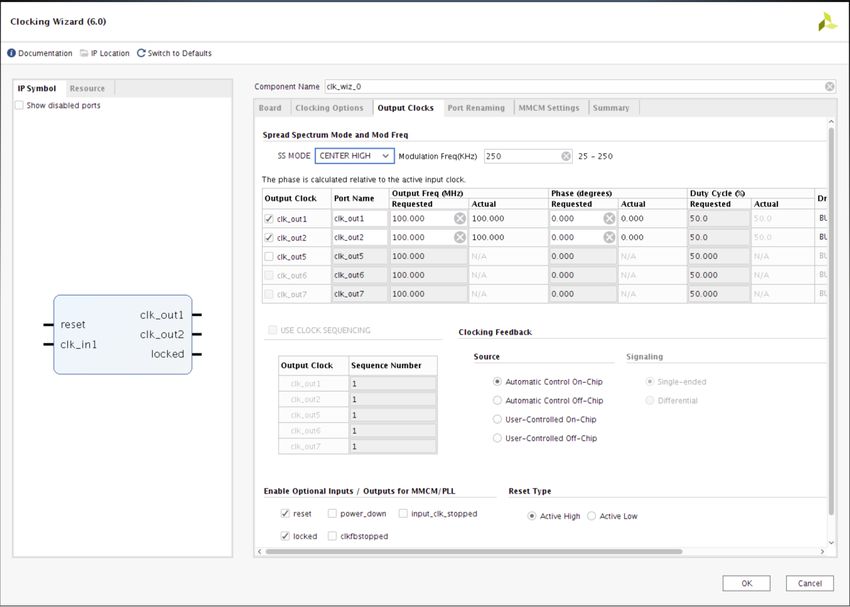
Output Clock Settings
The requirements for each selected output clock can be configured on the Output Clocks
tab in the IDE (Figure 4-4).
Clocking Wizard v6.0 Send Feedback
37
PG065 February 5, 2020 www.xilinx.comYou can also read