Video Mixer v5.2 LogiCORE IP Product Guide - Vivado Design Suite - Xilinx
←
→
Page content transcription
If your browser does not render page correctly, please read the page content below
Video Mixer v5.2

LogiCORE IP Product Guide

Vivado Design Suite
PG243 August 6, 2021
Table of Contents
       IP Facts

       Chapter 1: Overview
          Navigating Content by Design Process . . . . . . . . . . . . . . . . . . . . . . . . . . . . . . . . . . . . . . . . . . . . . . . . .                       5
          Feature Summary. . . . . . . . . . . . . . . . . . . . . . . . . . . . . . . . . . . . . . . . . . . . . . . . . . . . . . . . . . . . . . . . . .           5
          Applications . . . . . . . . . . . . . . . . . . . . . . . . . . . . . . . . . . . . . . . . . . . . . . . . . . . . . . . . . . . . . . . . . . . . . .     6
          Licensing and Ordering Information . . . . . . . . . . . . . . . . . . . . . . . . . . . . . . . . . . . . . . . . . . . . . . . . . . .                     6

       Chapter 2: Product Specification
          Standards . . . . . . . . . . . . . . . . . . . . . . . . . . . . . . . . . . . . . . . . . . . . . . . . . . . . . . . . . . . . . . . . . . . . . . . . 8
          Performance. . . . . . . . . . . . . . . . . . . . . . . . . . . . . . . . . . . . . . . . . . . . . . . . . . . . . . . . . . . . . . . . . . . . . . 8
          Resource Utilization. . . . . . . . . . . . . . . . . . . . . . . . . . . . . . . . . . . . . . . . . . . . . . . . . . . . . . . . . . . . . . . . 9
          Port Descriptions . . . . . . . . . . . . . . . . . . . . . . . . . . . . . . . . . . . . . . . . . . . . . . . . . . . . . . . . . . . . . . . . . 10
          Register Space . . . . . . . . . . . . . . . . . . . . . . . . . . . . . . . . . . . . . . . . . . . . . . . . . . . . . . . . . . . . . . . . . . . 20

       Chapter 3: Designing with the Core
          General Design Guidelines . . . . . . . . . . . . . . . . . . . . . . . . . . . . . . . . . . . . . . . . . . . . . . . . . . . . . . . . .                  31
          Clocking. . . . . . . . . . . . . . . . . . . . . . . . . . . . . . . . . . . . . . . . . . . . . . . . . . . . . . . . . . . . . . . . . . . . . . . . .    34
          Resets . . . . . . . . . . . . . . . . . . . . . . . . . . . . . . . . . . . . . . . . . . . . . . . . . . . . . . . . . . . . . . . . . . . . . . . . . .   34
          System Considerations . . . . . . . . . . . . . . . . . . . . . . . . . . . . . . . . . . . . . . . . . . . . . . . . . . . . . . . . . . . .                34
          Programming Sequence. . . . . . . . . . . . . . . . . . . . . . . . . . . . . . . . . . . . . . . . . . . . . . . . . . . . . . . . . . . .                  35

       Chapter 4: Design Flow Steps
          Customizing and Generating the Core . . . . . . . . . . . . . . . . . . . . . . . . . . . . . . . . . . . . . . . . . . . . . . . .                          36
          Constraining the Core . . . . . . . . . . . . . . . . . . . . . . . . . . . . . . . . . . . . . . . . . . . . . . . . . . . . . . . . . . . . .              42
          Simulation . . . . . . . . . . . . . . . . . . . . . . . . . . . . . . . . . . . . . . . . . . . . . . . . . . . . . . . . . . . . . . . . . . . . . .       42
          Synthesis and Implementation . . . . . . . . . . . . . . . . . . . . . . . . . . . . . . . . . . . . . . . . . . . . . . . . . . . . . .                     43

       Chapter 5: Example Design
          Simulation Example Design . . . . . . . . . . . . . . . . . . . . . . . . . . . . . . . . . . . . . . . . . . . . . . . . . . . . . . . . . 45
          Synthesizable Example Design . . . . . . . . . . . . . . . . . . . . . . . . . . . . . . . . . . . . . . . . . . . . . . . . . . . . . . 47

       Appendix A: Verification, Compliance, and Interoperability
          Simulation . . . . . . . . . . . . . . . . . . . . . . . . . . . . . . . . . . . . . . . . . . . . . . . . . . . . . . . . . . . . . . . . . . . . . . 58

Video Mixer v5.2                                                                                                                   Send Feedback
                                                                                                                                                                       2
PG243 August 6, 2021                                               www.xilinx.com
Hardware Testing. . . . . . . . . . . . . . . . . . . . . . . . . . . . . . . . . . . . . . . . . . . . . . . . . . . . . . . . . . . . . . . . . 58
          Interoperability . . . . . . . . . . . . . . . . . . . . . . . . . . . . . . . . . . . . . . . . . . . . . . . . . . . . . . . . . . . . . . . . . . 59

       Appendix B: Upgrading
          Upgrading in the Vivado Design Suite . . . . . . . . . . . . . . . . . . . . . . . . . . . . . . . . . . . . . . . . . . . . . . . . 60

       Appendix C: Application Software Development
          Building the BSP . . . . . . . . . . . . . . . . . . . . . . . . . . . . . . . . . . . . . . . . . . . . . . . . . . . . . . . . . . . . . . . . . .        63
          Prerequisites . . . . . . . . . . . . . . . . . . . . . . . . . . . . . . . . . . . . . . . . . . . . . . . . . . . . . . . . . . . . . . . . . . . .       63
          Modes of Operation. . . . . . . . . . . . . . . . . . . . . . . . . . . . . . . . . . . . . . . . . . . . . . . . . . . . . . . . . . . . . . .             64
          Usage . . . . . . . . . . . . . . . . . . . . . . . . . . . . . . . . . . . . . . . . . . . . . . . . . . . . . . . . . . . . . . . . . . . . . . . . . .   65

       Appendix D: Debugging
          Finding Help on Xilinx.com . . . . . . . . . . . . . . . . . . . . . . . . . . . . . . . . . . . . . . . . . . . . . . . . . . . . . . . . . 68
          Debug Tools . . . . . . . . . . . . . . . . . . . . . . . . . . . . . . . . . . . . . . . . . . . . . . . . . . . . . . . . . . . . . . . . . . . . . 69
          Hardware Debug . . . . . . . . . . . . . . . . . . . . . . . . . . . . . . . . . . . . . . . . . . . . . . . . . . . . . . . . . . . . . . . . . 70

       Appendix E: Additional Resources and Legal Notices
          Xilinx Resources . . . . . . . . . . . . . . . . . . . . . . . . . . . . . . . . . . . . . . . . . . . . . . . . . . . . . . . . . . . . . . . . . .        71
          Documentation Navigator and Design Hubs . . . . . . . . . . . . . . . . . . . . . . . . . . . . . . . . . . . . . . . . . . .                               71
          References . . . . . . . . . . . . . . . . . . . . . . . . . . . . . . . . . . . . . . . . . . . . . . . . . . . . . . . . . . . . . . . . . . . . . .      72
          Revision History . . . . . . . . . . . . . . . . . . . . . . . . . . . . . . . . . . . . . . . . . . . . . . . . . . . . . . . . . . . . . . . . . .        72
          Please Read: Important Legal Notices . . . . . . . . . . . . . . . . . . . . . . . . . . . . . . . . . . . . . . . . . . . . . . . .                        73

Video Mixer v5.2                                                                                                                  Send Feedback
                                                                                                                                                                      3
PG243 August 6, 2021                                               www.xilinx.com
IP Facts

                                                               •      Supports programmable CSC coefficient registers.
Introduction
                                                                                    LogiCORE™ IP Facts Table
The Xilinx® LogiCORE™ IP Video Mixer core                                                 Core Specifics
provides a flexible video processing block for alpha
                                                                                                              UltraScale+™ Families
blending and compositing multiple video and/or
                                                                   Supported                               UltraScale™ Architecture
graphics layers. Support for up to seventeen layers                Device Family(1)                                Zynq®-7000 SoC
(one main layer and sixteen overlay layers), with an                                                                 7 Series FPGAs
optional logo layer, using a combination of video
                                                                   Supported User
inputs from either memory or streaming video cores                 Interfaces
                                                                                              AXI4-Master, AXI4-Lite, AXI4-Stream(2)
(through AXI4-Stream interfaces) is provided. The
                                                                                        Performance and Resource Utilization web
core is programmable through a comprehensive                       Resources
                                                                                                                            page
register interface to control frame size, background
color, layer position, and the AXI4-Lite interface. A                                  Provided with Core
comprehensive set of interrupt status bits is                      Design Files                                       Not Provided
provided for processor monitoring.
                                                                   Example Design                                               Yes

Features                                                           Test Bench
                                                                   Constraints File
                                                                                                                      Not Provided
                                                                                                     Xilinx Design Constraints (XDC)

•   Supports (per pixel) alpha-blending of seventeen               Simulation
                                                                                                                      Encrypted RTL
                                                                   Model
    video/graphics and logo layers video/graphics
                                                                   Supported                                            Standalone
•   Optional logo (in block RAM) layer with color                  S/W Driver (3)                                        DRM/KMS
    transparency support
                                                                                      Tested Design Flows(4)
•   Layers can either be memory mapped AXI4
                                                                   Design Entry                               Vivado® Design Suite
    interface or AXI4-Stream
                                                                                                   For supported simulators, see the
•   Provides programmable background color                         Simulation
                                                                                         Xilinx Design Tools: Release Notes Guide.
•   Provides programmable layer position and size                  Synthesis                                       Vivado Synthesis
•   Provides upscaling of layers by 1x, 2x, or 4x                  Release Notes
•   Optional built-in color space conversion and                   and Known                       Master Answer Record: AR 66753
                                                                   Issues
    chroma re-sampling
                                                                   All Vivado IP
•   Supports RGB, YUV 444, YUV 422, YUV 420                                                   Master Vivado IP Change Logs: 72775
                                                                   Change Logs
•   Supports 8, 10, 12, and 16 bits per color
    component input and output on stream interface,
                                                                                             Support
    8-bit and 10-bit per color component on memory                        Provided by Xilinx at the Xilinx Support web page
    interface
                                                               Notes:
•   Supports semi-planar memory formats next to                1. For a complete list of supported devices, see the Vivado IP
    packed memory formats                                         catalog.
•   Supports spatial resolutions from 64 × 64 up to            2. Video protocol as defined in the AXI4-Stream Video IP and
                                                                  System Design Guide (UG934) [Ref 2].
    8,192 × 4,320
                                                               3. Standalone driver details can be found in /
•   Supports 8K30 in all supported device families (1)            Vitis//data/embeddedsw/doc/
                                                                  xilinx_drivers_api_toc.htm. Linux OS and driver support
•   Supports Programmable CSC coefficients to                     information is available from the
    support various calorimetry like BT601, BT709 and             Xilinx Wiki page.
    BT2020.                                                    4. For the supported versions of the tools, see the
                                                                  Xilinx Design Tools: Release Notes Guide.

1. Performance on low power devices might be lower.

Video Mixer v5.2                                                                                Send Feedback                4
PG243 August 6, 2021                                  www.xilinx.com                                     Product Specification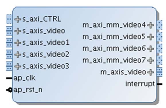
Chapter 1

Overview
       The Xilinx® LogiCORE™ IP Video Mixer produces one single output video stream from
       multiple external video and/or graphics sources. Sources can be dynamically positioned,
       scaled, and combined using alpha-blending.

       Navigating Content by Design Process
       Xilinx® documentation is organized around a set of standard design processes to help you
       find relevant content for your current development task. This document covers the
       following design processes:

       •   Hardware, IP, and Platform Development: Creating the PL IP blocks for the hardware
           platform, creating PL kernels, subsystem functional simulation, and evaluating the
           Vivado timing, resource and power closure. Also involves developing the hardware
           platform for system integration. Topics in this document that apply to this design
           process include:

           °   Port Descriptions

           °   Register Space

           °   Clocking

           °   Resets

           °   Customizing and Generating the Core

           °   Example Design

       Feature Summary
       The Video Mixer is a highly configurable IP core that supports blending of up to seventeen
       video and/or graphics layers plus an additional logo layer into one single output video
       stream. All layers except the master layer can either be a memory mapped AXI4 interface or
       AXI4-Stream based. Alpha-blending (global or per pixel) and scaling is supported per layer.
       Finally, built-in color space conversion between RGB and YUV 4:4:4 and chroma re-sampling
       between YUV 4:4:4, YUV 4:2:2, and YUV 4:2:0 is optionally available.

Video Mixer v5.2                                                            Send Feedback
                                                                                                 5
PG243 August 6, 2021                     www.xilinx.com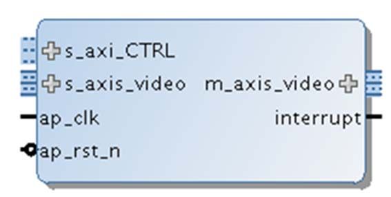
Chapter 1: Overview

       The mixer provides an optional logo layer. It blends a logo that is stored in block RAM on
       the top-most layer. A programmable color key can be used to make part of the logo
       transparent. Also, alpha-blending (global or per pixel) can be used for logo transparency.

       Alpha-blending is the convex combination of two image layers allowing for transparency.
       Each layer in the mixer has a fixed Z-plane order; or conceptually, each layer resides closer
       to the observer having a different depth. Thus, the image and the image directly "over" it
       are blended. The order and amount of blending is programmable in real-time. This can
       either be done through a global alpha, that is, every pixel uses the same alpha value, or
       through a per pixel alpha value in case either the RGBA8, BGRA8, or YUVA8 memory video
       format is selected. Per pixel alpha also supports RGBA and YUVA444 streaming video
       formats.

       Scaling by means of pixel and line repeat is supported, and provides scaling of layers by 1x,
       2x, or 4x. This feature might be used to save on memory bandwidth used by a layer, that is,
       a memory layer can read in a 1,920 × 1,080 frame buffer while scaling it up on-the-fly to a
       3,840 × 2,160 resolution.

       The Video Mixer supports parallel processing of multiple pixels per clock cycle allowing
       support for resolutions beyond 1080p60 with up to three color components, each of 8, 10,
       12, or 16 bits.

       Applications
       Applications range from broadcast and consumer, automotive, medical and industrial
       imaging, and can include the following:

       •   Video surveillance
       •   Machine vision
       •   Video conferencing
       •   Set-top box displays

       Licensing and Ordering Information
       This Xilinx LogiCORE™ IP module is provided at no additional cost with the Xilinx Vivado
       Design Suite under the terms of the Xilinx End User License. Information about this and
       other Xilinx LogiCORE IP modules is available at the Xilinx Intellectual Property page. For
       information about pricing and availability of other Xilinx LogiCORE IP modules and tools,
       contact your local Xilinx sales representative.

       For more information, visit the Video Mixer product web page.

Video Mixer v5.2                                                              Send Feedback
                                                                                                     6
PG243 August 6, 2021                      www.xilinx.com
Chapter 1: Overview
Information about other Xilinx LogiCORE IP modules is available at the Xilinx Intellectual
Property page. For information on pricing and availability of other Xilinx LogiCORE IP
modules and tools, contact your local Xilinx sales representative.
Video Mixer v5.2 Send Feedback
7
PG243 August 6, 2021 www.xilinx.comChapter 2
Product Specification
Standards
The Video Mixer is compliant with the AXI4-Stream Video Protocol, AXI4-Lite interconnect
and memory mapped AXI4 interface standards. For additional information, see the “Video
IP: AXI Feature Adoption” section of the AXI4-Stream Video IP and System Design Guide
(UG934) [Ref 2].
Performance
The following sections detail the performance characteristics of the Video Mixer.
Maximum Frequencies
The following are typical clock frequencies for the target devices:
• Virtex ®-7 and Virtex UltraScale™ devices with –2 speed grade or higher: 300 MHz
• Kintex®-7 and Kintex UltraScale™ devices with –2 speed grade or higher: 300 MHz
• Artix ®-7 devices with –2 speed grade or higher: 150 MHz
• UltraScale™+ devices with -1 speed grade or higher: 300 MHz
• Versal™ ACAP devices with -1 Speed grade or higher: 300 MHz
The maximum achievable clock frequency can vary. The maximum achievable clock
frequency and all resource counts can be affected by other tool options, additional logic in
the device, using a different version of Xilinx ® tools, and other factors.
Throughput
The Video Mixer supports bi-directional data throttling between its AXI4-Stream slave and
master interfaces. If the slave side data source is not providing valid data samples
(s_axis_video_tvalid is not asserted), the core cannot produce valid output samples
after its internal buffers are depleted. Similarly, if the master side interface is not ready to
Video Mixer v5.2 Send Feedback
8
PG243 August 6, 2021 www.xilinx.comChapter 2: Product Specification
accept valid data samples (m_axis_video_tready is not asserted) the core cannot
accept valid input samples after its buffers become full.
If the master interface is able to provide valid samples (s_axis_video_tvalid is High)
and the slave interface is ready to accept valid samples (m_axis_video_tready is High),
typically the core can process and produce one, two, or four pixels specified by Samples
Per Clock in the Vivado® Integrated Design Environment (IDE) per ap_clk cycle.
However, at the end of each scan line and frame the core flushes internal pipelines for
several clock cycles, during which the s_axis_video_tready is deasserted signaling that
the core is not ready to process samples.
When the Video Mixer is processing timed streaming video (which is typical for most video
sources), the flushing periods coincide with the blanking periods and therefore do not
reduce the throughput of the system.
When operating on a streaming video source (that is, not frame buffered data), the Video
Mixer must operate minimally at the burst data rate. For example, 148.5 MHz for a 1080p60
video source for a one sample per clock configuration of the IP. For a 4K 60 fps video source,
the core must operate at 297 MHz for a two sample per clock configuration, or 148.5 MHz
for a four sample per clock configuration on slower devices such as Artix ®-7.
Resource Utilization
For full details about performance and resource utilization, visit the Performance and
Resource Utilization web page.
Video Mixer v5.2 Send Feedback
9
PG243 August 6, 2021 www.xilinx.comChapter 2: Product Specification
Port Descriptions
The Video Mixer uses industry standard control and data interfaces to connect to other
system components. The following sections describe the various interfaces available with
the core. Figure 2-1 illustrates a Video Mixer I/O diagram. In this configuration, the IP has
10 AXI interfaces:
• AXI4-Lite control interface (s_axi_CTRL)
• AXI4-Stream streaming video output (m_axis_video)
• AXI4-Stream streaming video input (s_axis_video, s_axis_video1, etc.)
• Memory mapped AXI4 interface (m_axi_mm_video4, m_axi_mm_video5, etc.).
X-Ref Target - Figure 2-1
Figure 2-1: Video Mixer I/O Diagram
Video Mixer v5.2 Send Feedback
10
PG243 August 6, 2021 www.xilinx.comChapter 2: Product Specification
The interfaces change depending on the number of layers and layer type, that is, streaming
or memory based. For example, Figure 2-2 shows a minimum configuration of the Video
Mixer IP with only one layer and a logo layer.
X-Ref Target - Figure 2-2
Figure 2-2: Video Mixer I/O Diagram Single Layer
Common Interface Signals
Table 2-1 summarizes the signals which are either shared by, or not part of the dedicated
AXI4-Stream, memory mapped AXI4 data, or AXI4-Lite control interfaces.
Table 2-1: Common Interface Signals
Signal Name I/O Width Description
ap_clk I 1 Video core clock
ap_rst_n I 1 Video core active-Low reset
interrupt O 1 Interrupt Request Pin
The ap_clk and ap_rst_n signals are shared between the core, the AXI4-Stream, memory
mapped AXI4 data interfaces, and the AXI4-Lite control interface.
ap_clk
The AXI4-Stream, memory mapped AXI4, and AXI4-Lite interfaces must be synchronous to
the core clock signal ap_clk. All AXI4-Stream, memory mapped AXI4 interface input
signals and AXI4-Lite control interface input signals are sampled on the rising edge of
ap_clk. All AXI4-Stream output signal changes occur after the rising edge of ap_clk.
ap_rst_n
The ap_rst_n pin is an active-Low, synchronous reset input pertaining to both AXI4-Lite,
AXI4-Stream, and memory mapped AXI4 interfaces. When ap_rst_n is set to 0, the core
resets at the next rising edge of ap_clk.
Video Mixer v5.2 Send Feedback
11
PG243 August 6, 2021 www.xilinx.comChapter 2: Product Specification
interrupt
The interrupt status output bus can be integrated with an external interrupt controller that
has independent interrupt enable/mask, interrupt clear, and interrupt status registers that
allows for interrupt aggregation to the system processor.
AXI4-Stream Video Interface
The Video Mixer in any configuration has AXI4-Stream video input and output interfaces
named s_axis_video and m_axis_video, respectively. Per additional streaming layer,
there are an additional AXI4-Stream video input named s_axis_videoi with i
representing the layer number minus 1. All video streaming interfaces follow the interface
specification as defined in the AXI4-Stream Video IP and System Design Guide (UG934)
[Ref 2]. The video AXI4-Stream interface can be single, dual, or quad pixels per clock and
can support 8, 10, 12, or 16 bits per component. The streaming interface configuration
(samples per clock and bits per component) is chosen at IP level and applies to all instances
of the AXI4-Stream interface.
Table 2-2 through Table 2-6 explain the pixel mapping of an AXI4-Stream interface with 2
pixels per clock and 10 bits per component configuration for all supported color formats.
Given that the Video Mixer always requires a hardware configuration for at least three
component video, the AXI4-Stream Subset Converter is needed to communicate with other
IPs of two or one component video interface in YUV 4:2:2, 4:2:0, or Luma Only.
Table 2-2: Dual Pixels Per Clock, 10 Bits Per Component Mapping for RGB
63:60 59:50 49:40 39:30 29:20 19:10 9:0
Zero padding R1 B1 G1 R0 B0 G0
Table 2-3: Dual Pixels Per Clock, 10 Bits Per Component Mapping for YUV 4:4:4
63:60 59:50 49:40 39:30 29:20 19:10 9:0
Zero padding V1 U1 Y1 V0 U0 Y0
Table 2-4: Dual Pixels Per Clock, 10 Bits Per Component Mapping for YUV 4:2:2
63:60 59:50 49:40 39:30 29:20 19:10 9:0
Zero padding Zero padding Zero padding V0 Y1 U0 Y0
Table 2-5: Dual Pixels Per Clock, 10 Bits Per Component Mapping for RGBA
79:70 69:60 59:50 49:40 39:30 29:20 19:10 9:0
A1 R1 B1 G1 A0 R0 B0 G0
Table 2-6: Dual Pixels Per Clock, 10 Bits Per Component Mapping for YUVA 4:4:4
79:70 69:60 59:50 49:40 39:30 29:20 19:10 9:0
A1 V1 U1 Y1 A0 V0 U0 Y0
Video Mixer v5.2 Send Feedback
12
PG243 August 6, 2021 www.xilinx.comChapter 2: Product Specification
Table 2-7 shows the interface signals for input and output AXI4-Stream video streaming
interfaces.
Table 2-7: AXI4-Stream Interface Signals
Signal Name I/O Width Description
(1)
floor(((3 × bits_per_component
s_axis_tdata I Input Data
× pixels_per_clock) + 7) / 8) × 8
s_axis_tready O 1 Input Ready
s_axis_tvalid O 1 Input Valid
s_axis_tdest I 1 Input Data Routing Identifier
Input byte qualifier that indicates whether the
s_axis_tkeep I (s_axis_video_tdata width) / 8 content of the associated byte of TDATA is
processed as part of the data stream.
s_axis_tlast I 1 Input End of Line
Input byte qualifier that indicates whether the
s_axis_tstrb I (s_axis_video_tdata width) / 8 content of the associated byte of TDATA is
processed as a data byte or a position byte.
s_axis_tuser I 1 Input Start of Frame
floor(((3 × bits_per_component
m_axis_tdata O Output Data
× pixels_per_clock) + 7) / 8) × 8
m_axis_tdest O 1 Output Data Routing Identifier
m_axis_tid O 1 Output Data Stream Identifier
Output byte qualifier that indicates whether the
m_axis_tkeep O (m_axis_video_tdata width) / 8 content of the associated byte of TDATA is
processed as part of the data stream.
m_axis_tlast O 1 Output End of Line
m_axis_tready I 1 Output Ready
Output byte qualifier that indicates whether the
m_axis_tstrb O (m_axis_video_tdata width) / 8 content of the associated byte of TDATA is
processed as a data byte or a position byte.
m_axis_tuser O 1 Output Start of Frame
m_axis_tvalid O 1 Output Valid
Notes:
1. For RGBA and YUVA444, the video data consists of 4 components.
All video streaming interfaces run at the IP core clock speed, ap_clk.
Video Mixer v5.2 Send Feedback
13
PG243 August 6, 2021 www.xilinx.comChapter 2: Product Specification
Memory Mapped AXI4 Interface
Per memory layer, there is a memory mapped AXI4 interface named m_axi_mm_videoi
with i representing the layer number minus 1. The memory mapped AXI4 interface runs on
the ap_clk clock domain. The signals follow the specification as defined in the Vivado
Design Suite: AXI Reference Guide (UG1037) [Ref 1]. Table 2-8 shows the pixel formats in
memory supported by the Video Mixer.
Table 2-8: Pixel Formats
Video Format Description Bits per Component Bytes per Pixel
RGBX8 packed RGB 8 4 bytes per pixel
BGRX8 packed BGR 8 4 bytes per pixel
YUVX8 packed YUV 4:4:4 8 4 bytes per pixel
YUYV8 packed YUV 4:2:2 8 2 bytes per pixel
UYVY8 packed YUV 4:2:2 8 2 bytes per pixel
RGBA8 packed RGB with alpha 8 4 bytes per pixel
BGRA8 packed BGR with alpha 8 4 bytes per pixel
YUVA8 packed YUV 4:4:4 8 4 bytes per pixel
RGBX10 packed RGB 10 4 bytes per pixel
YUVX10 packed YUV 4:4:4 10 4 bytes per pixel
RGB565 packed RGB 5 bits per R component 2 bytes per pixel
6 bits per G component
5 bits per B component
BGR8 packed BGR 8 3 bytes per pixel
Y_UV8 semi-planar YUV 4:2:2 8 1 byte per pixel per plane
Y_UV8_420 semi-planar YUV 4:2:0 8 1 byte per pixel per plane
RGB8 packed RGB 8 3 bytes per pixel
YUV8 packed YUV 4:4:4 8 3 bytes per pixel
Y_UV10 semi-planar YUV 4:2:2 10 4 bytes per 3 pixels per plane
Y_UV10_420 semi-planar YUV 4:2:0 10 4 bytes per 3 pixels per plane
Y8 packed luma only 8 1 byte per pixel
Y10 packed luma only 10 4 bytes per 3 pixels
The following tables explain the expected pixel mappings in memory for each of the
mentioned listed formats.
Video Mixer v5.2 Send Feedback
14
PG243 August 6, 2021 www.xilinx.comChapter 2: Product Specification
RGBX8
Packed RGB, 8 bits per component. Every pixel in memory is represented with 32 bits, as
shown. The images need be stored in memory in raster order, that is, top-left pixel first,
bottom-right pixel last. Bits[31:24] do not contain pixel information.
31:24 23:16 15:8 7:0
X B G R
YUVX8
Packed YUV 4:4:4, 8 bits per component. Every pixel in memory is represented with 32 bits,
as shown. Bits[31:24] do not contain pixel information.
31:24 23:16 15:8 7:0
X V U Y
BGRX8
Packed BGR, 8 bits per component. Every pixel in memory is represented with 32 bits, as
shown. The images need be stored in memory in raster order, that is, top-left pixel first,
bottom-right pixel last. Bits[31:24] do not contain pixel information.
31:24 23:16 15:8 7:0
X R G B
YUYV8
Packed YUV 4:2:2, 8 bits per component. Every two pixels in memory are represented with
32 bits, as shown.
31:24 23:16 15:8 7:0
V0 Y1 U0 Y0
RGBA8
Packed RGB with alpha, 8 bits per component. Every pixel is represented with 32 bits, as
shown. Bits[31:24] contain alpha information, 0 is fully transparent, 255 is fully opaque.
31:24 23:16 15:8 7:0
A B G R
Video Mixer v5.2 Send Feedback
15
PG243 August 6, 2021 www.xilinx.comChapter 2: Product Specification
UYVY8
Packed YUV 4:2:2, 8 bits per component. Every two pixels in memory are represented with
32 bits, as shown:
31:24 23:16 15:8 7:0
Y1 V0 Y0 U0
BGRA8
Packed BGR with alpha, 8 bits per component. Every pixel is represented with 32 bits, as
shown. Bits[31:24] contain alpha information, 0 is fully transparent, 255 is fully opaque.
31:24 23:16 15:8 7:0
A R G B
YUVA8
Packed YUV with alpha, 8 bits per component. Every pixel is represented with 32 bits, as
shown. Bits[31:24] contain alpha information, 0 is fully transparent, 255 is fully opaque.
31:24 23:16 15:8 7:0
A V U Y
RGBX10
Packed RGB, 10 bits per component. Every pixel is represented with 32 bits, as shown.
Bits[31:30] do not contain any pixel information.
31:30 29:20 19:10 9:0
X B G R
YUVX10
Packed YUV 4:4:4, 10 bits per component. Every pixel is represented with 32 bits, as shown.
Bits[31:30] do not contain any pixel information.
31:30 29:20 19:10 9:0
X V U Y
Video Mixer v5.2 Send Feedback
16
PG243 August 6, 2021 www.xilinx.comChapter 2: Product Specification
RGB565
Packed RGB with 5 bits per R component, 6 bits per G component, 5 bits per B component.
Every pixel is represented with 16 bits, as shown.
15:11 10:5 4:0
B G R
Y_UV8
Semi-planar YUV 4:2:2 with 8 bits per component. Y and UV stored in separate planes as
shown. The UV plane is assumed to have an offset of stride × height bytes from the Y plane
buffer address.
31:24 23:16 15:8 7:0
Y3 Y2 Y1 Y0
31:24 23:16 15:8 7:0
V2 U2 V0 U0
Y_UV8_420
Semi-planar YUV 4:2:0 with 8 bits per component. Y and UV stored in separate planes as
shown. The UV plane is assumed to have an offset of stride × height bytes from the Y plane
buffer address.
31:24 23:16 15:8 7:0
Y3 Y2 Y1 Y0
31:24 23:16 15:8 7:0
V4 U4 V0 U0
RGB8
Packed RGB, 8 bits per component. Every pixel in memory is represented with 24 bits, as
shown. The images need be stored in memory in raster order, that is, top-left pixel first,
bottom-right pixel last.
23:16 15:8 7:0
B G R
Video Mixer v5.2 Send Feedback
17
PG243 August 6, 2021 www.xilinx.comChapter 2: Product Specification
BGR8
Packed BGRB, 8 bits per component. Every pixel in memory is represented with 24 bits, as
shown. The images need be stored in memory in raster order, that is, top-left pixel first,
bottom-right pixel last.
23:16 15:8 7:0
R G B
YUV8
Packed YUV 4:4:4, 8 bits per component. Every pixel in memory is represented with 24 bits,
as shown. The images need be stored in memory in raster order, that is, top-left pixel first,
bottom-right pixel last.
23:16 15:8 7:0
V U Y
Y_UV10
Semi-planar YUV 4:2:2 with 10 bits per component. Every 3 pixels is represented with 32
bits. Bits[31:30] do not contain any pixel information. Y and UV stored in separate planes as
shown. The UV plane is assumed to have an offset of stride x height bytes from the Y plane
buffer address.
63:62 61:52 51:42 41:32 31:30 29:20 19:10 9:0
X Y5 Y4 Y3 X Y2 Y1 Y0
63:62 61:52 51:42 41:32 31:30 29:20 19:10 9:0
X V4 U4 V2 X U2 V0 U0
Y_UV10_420
Semi-planar YUV 4:2:0 with 10 bits per component. Every 3 pixels is represented with 32
bits. Bits[31:30] do not contain any pixel information. Y and UV stored in separate planes as
shown. The UV plane is assumed to have an offset of stride x height bytes from the Y plane
buffer address.
63:62 61:52 51:42 41:32 31:30 29:20 19:10 9:0
X Y5 Y4 Y3 X Y2 Y1 Y0
63:62 61:52 51:42 41:32 31:30 29:20 19:10 9:0
X V8 U8 V4 X U4 V0 U0
Video Mixer v5.2 Send Feedback
18
PG243 August 6, 2021 www.xilinx.comChapter 2: Product Specification
Y8
Packed Luma-Only, 8 bits per component. Every luma-only pixel in memory is represented
with 8 bits, as shown. The images need be stored in memory in raster order, that is, top-left
pixel first, bottom-right pixel last. Y8 is presented as YUV 4:4:4 on the AXI4-Stream
interface.
7:0
Y
Y10
Packed Luma-Only, 10 bits per component. Every three luma-only pixels in memory is
represented with 32 bits, as shown. The images need be stored in memory in raster order,
that is, top-left pixel first, bottom-right pixel last. Y10 is presented as YUV 4:4:4 on the
AXI4-Stream interface.
31:30 29:20 19:10 9:0
X Y2 Y1 Y0
AXI4-Lite Control Interface
The AXI4-Lite interface allows you to dynamically control parameters within the core. The
configuration can be accomplished using an AXI4-Lite master state machine, an embedded
ARM ®, or soft system processor such as MicroBlaze™. The Video Mixer can be controlled
through the AXI4-Lite interface by using functions provided by the driver in the Vitis.
Another method is performing read and write transactions to the register space but should
only be used when the first method is not available. Table 2-9 shows the AXI4-Lite control
interface signals. This interface runs at the ap_clk clock.
Table 2-9: AXI4-Lite Control Interface Signals
Signal Name I/O Width Description
s_axi_ctrl_aresetn I 1 Reset
s_axi_ctrl_aclk I 1 Clock
s_axi_ctrl_awaddr I 18 Write Address
s_axi_ctrl_awprot I 3 Write Address Protection
s_axi_ctrl_awvalid I 1 Write Address Valid
s_axi_ctrl_awready O 1 Write Address Ready
s_axi_ctrl_wdata I 32 Write Data
s_axi_ctrl_wstrb I 4 Write Data Strobe
s_axi_ctrl_wvalid I 1 Write Data Valid
s_axi_ctrl_wready O 1 Write Data Ready
Video Mixer v5.2 Send Feedback
19
PG243 August 6, 2021 www.xilinx.comChapter 2: Product Specification
Table 2-9: AXI4-Lite Control Interface Signals (Cont’d)
Signal Name I/O Width Description
s_axi_ctrl_bresp O 2 Write Response
s_axi_ctrl_bvalid O 1 Write Response Valid
s_axi_ctrl_bready I 1 Write Response Ready
s_axi_ctrl_araddr I 18 Read Address
s_axi_ctrl_arprot I 3 Read Address Protection
s_axi_ctrl_arvalid I 1 Read Address Valid
s_axi_ctrl_aready O 1 Read Address Ready
s_axi_ctrl_rdata O 32 Read Data
s_axi_ctrl_rresp O 2 Read Data Response
s_axi_ctrl_rvalid O 1 Read Data Valid
s_axi_ctrl_rready I 1 Read Data Ready
Register Space
The Video Mixer has specific registers which allow you to dynamically control the operation
of the core. All registers have an initial value of 0.
Top-Level Registers
Table 2-10 provides a detailed description of all the registers that apply globally to the IP.
Table 2-10: Top-Level Registers
Address (hex) Access
BASEADDR+ Register Name Type Register Description
Bit[0] = ap_start
Bit[1] = ap_done
Bit[2] = ap_idle
Bit[3] = ap_ready
0x0000 Control R/W
Bit[5] = Flush pending AXI transactions (2)
Bit[6] = Flush done
Bit[7] = auto_restart
Others = Reserved
Bit[0] = Global interrupt enable
0x0004 Global Interrupt Enable R/W
Others = Reserved
Bit[0] = ap_done
0x0008 IP Interrupt Enable Bit[1] = ap_ready
Others = reserved
Video Mixer v5.2 Send Feedback
20
PG243 August 6, 2021 www.xilinx.comChapter 2: Product Specification
Table 2-10: Top-Level Registers (Cont’d)
Address (hex) Register Name Access Register Description
BASEADDR+ Type
Bit[0] = ap_done
IP Interrupt Status
0x000C R/TOW(1) Bit[1] = ap_ready
Register
Others = Reserved
0x0010 Width R/W Active width of background.
0x0018 Height R/W Active height of background.
0x0028 Background_Y_R R/W Red or Y value of background color
0x0030 Background_U_G R/W Green or U value of background color
0x0038 Background_V_B R/W Blue or V value of background color
Bit[0] = Master layer is enabled/disabled
Bit[1] = Overlay Layer 1 is enabled/disabled
0x0040 Layer enable R/W …
Bit[16] = Overlay Layer 16 is enabled/disabled
Bit[23] = Logo layer is enabled/disabled
Notes:
1. TOW = Toggle on Write.
2. BIT[5] and BIT[6] are applicable only for memory based layers.
Control (0x0000) Register
This register controls the operation of the Video Mixer. Bit[0] of the Control register,
ap_start, kicks off the core from software. Writing 1 to this bit, starts the core to generate
a video frame. Bit[5] is for flushing pending AXI transactions. Bit[5] should be set and held
(until reset) by software to flush pending transactions. When Bit[5] is set, the hardware
expects a hard reset. Bit[6] is the flush status bit and is asserted when the flush is done. To
set the core in free running mode, Bit[7] of this register, auto_restart, must be set to 1.
Bits[3:1] are not used now but reserved for future use.
Global Interrupt Enable (0x0004) Register
This register is the master control for all interrupts. Bit[0] can be used to enable/disable all
core interrupts.
IP Interrupt Enable (0x0008) Register
This register allows interrupts to be enabled selectively. Currently, two interrupt sources are
available ap_done and ap_ready. ap_done is triggered after the frame processing is
complete, while ap_ready is triggered after the core is ready to start processing the next
frame.
Video Mixer v5.2 Send Feedback
21
PG243 August 6, 2021 www.xilinx.comChapter 2: Product Specification
IP Interrupt Status (0x000C) Register
This is a dual purpose register. When an interrupt occurs, the corresponding interrupt
source bit is set in this register. In readback mode (Get status), the interrupting source can
be determined. In writeback mode (Clear interrupt), the requested interrupt source bit is
cleared.
Width (0x0010) Register
The WIDTH register encodes the number of active pixels per scan. Supported values are
between 64 and the value provided in the Maximum Number of Columns field in the
Vivado Integrated Design Environment (IDE). To avoid processing errors, you should restrict
values written to width to the range supported by the core instance. Furthermore, width
needs to be a multiple of the Samples per Clock field in the Vivado® IDE.
Height (0x0018) Register
The Height register encodes the number of active scan lines per frame. Supported values
are between 64 and the value provided in the Maximum Number of Rows field in the
Vivado IDE. To avoid processing errors, you should restrict values written to height to the
range supported by the core instance.
Background_Y_R (0x0028) Register
Red color component of the background color. The range of the background color is
determined by the number of bits per color component selected in the Maximum Data
Width field in the Vivado IDE, for example, 0..1023 for 10-bit maximum data width.
Background_U_G (0x0030) Register
Green color component of the background color. The range of the background color is
determined by the number of bits per color component selected in the Maximum Data
Width field in the Vivado IDE, for example, 0..1023 for 10-bit maximum data width.
Background_V_B (0x0038) Register
Blue color component of the background color. The range of the background color is
determined by the number of bits per color component selected in the Maximum Data
Width field in the Vivado IDE, for example, 0..1023 for 10-bit maximum data width.
Layer Enable (0x0040) Register
This register has one bit for every layer that indicates whether a layer is enabled (1) or
disabled (0). Bit[0] is for the master input layer, which associates with the s_axis_video
AXI4-Stream input. This is the bottom-most layer, and all other layers are blended on top.
If this layer is disabled and no other layers are blended on top, the background color as
Video Mixer v5.2 Send Feedback
22
PG243 August 6, 2021 www.xilinx.comChapter 2: Product Specification
specified by the previous mentioned registers are shown. If this layer is enabled, video data
should be sent to this layer, otherwise the Video Mixer stalls.
Bit[1] is for overlay layer 1, which associates with either s_axis_video1 AXI4-Stream
input or m_axi_mm_video1 memory mapped AXI4 input, depending on the Interface
Type field selected in the Vivado IDE. Bit[2] is for overlay layer 2, and so on, until Bit[16]
which enables/disables layer 16.
Bit[23] is for the logo layer. The logo layer is the top-most layer and is blended on top of all
other layers.
CSC Coefficient Registers
Table 2-11 provides a detailed description of CSC coefficient registers:
Note: These registers are available to program only if the Enable CSC Coefficient Registers option
is enabled in the GUI. With these registers, different CSC coefficients can be programmed to support
BT601, BT709 and BT2020.
Table 2-11: CSC Coefficient Registers
Address (hex) Register Access
BASEADDR+ Name Type Description
0x00048 K11 R/W 16 Bits K11[15:0] are Read/Write and others are reserved
0x00050 K12 R/W 16 Bits K12[15:0] are Read/Write and others are reserved
0x00058 K13 R/W 16 Bits K13[15:0] are Read/Write and others are reserved
0x00060 K21 R/W 16 Bits K21[15:0] are Read/Write and others are reserved
0x00068 K22 R/W 16 Bits K22[15:0] are Read/Write and others are reserved
0x00070 K23 R/W 16 Bits K23[15:0] are Read/Write and others are reserved
0x00078 K31 R/W 16 Bits K31[15:0] are Read/Write and others are reserved
0x00080 K32 R/W 16 Bits K32[15:0] are Read/Write and others are reserved
0x00088 K33 R/W 16 Bits K33[15:0] are Read/Write and others are reserved
0x00090 ROffset R/W 12 Bits ROffset[11:0] are Read/Write and others are reserved
0x00098 GOffset R/W 12 Bits GOffset[11:0] are Read/Write and others are reserved
0x000A0 Boffset R/W 12 Bits BOffset[11:0] are Read/Write and others are reserved
0x00140 K11_2 R/W 16 Bits K11_2[15:0] are Read/Write and others are reserved
0x00148 K12_2 R/W 16 Bits K12_2[15:0] are Read/Write and others are reserved
0x00150 K13_2 R/W 16 Bits K13_2[15:0] are Read/Write and others are reserved
0x00158 K21_2 R/W 16 Bits K21_2[15:0] are Read/Write and others are reserved
0x00160 K22_2 R/W 16 Bits K22_2[15:0] are Read/Write and others are reserved
0x00168 K23_2 R/W 16 Bits K23_2[15:0] are Read/Write and others are reserved
0x00170 K31_2 R/W 16 Bits K31_2[15:0] are Read/Write and others are reserved
0x00178 K32_2 R/W 16 Bits K32_2[15:0] are Read/Write and others are reserved
Video Mixer v5.2 Send Feedback
23
PG243 August 6, 2021 www.xilinx.comChapter 2: Product Specification
Table 2-11: CSC Coefficient Registers (Cont’d)
Address (hex) Register Access Description
BASEADDR+ Name Type
0x00180 K33_2 R/W 16 Bits K33_2[15:0] are Read/Write and others are reserved
0x00188 YOffset R/W 12 Bits YOffset[11:0] are Read/Write and others are reserved
0x00190 UOffset R/W 12 Bits UOffset[11:0] are Read/Write and others are reserved
0x00198 VOffset R/W 12 Bits VOffset[11:0] are Read/Write and others are reserved
Notes:
1. These registers can be used to program your coefficients.
2. For YUV to RGB and RGB to YUV equations, refer to CSC section of Video Processing Subsystem PG231 [Ref 11]
Layer Registers
Table 2-12 provides a detailed description of all the registers that apply to layers 0 through
16. Note that overlay layer 1 registers start at base address 0x0200, overlay layer 2 registers
start at base address 0x300, and so forth.
Mixer IP has one primary layer, which we mention as layer0. It supports up to 16 overlay
layers (Layer 1 to Layer 16). Layer 0 does not have any register for programming. For all
overlay layers (Layer 1 to Layer 16) the registers are at identical offsets. Layer 1 registers
start at base address 0x200, Layer 2 registers start at base address 0x300 and so forth. Layer
16 registers start at base address 0x1100. In this section, the register description number
represents a number from 2 to 11.
Table 2-12: Layer Registers
Address (hex) Register Access Description
BASEADDR+ Name Type
Alpha blending value for layer 1 ranging from
Layer 1
0x0200 R/W 0 = Fully transparent
Alpha
256 = Fully opaque
Layer 1 X position of the top left corner of layer 1, relative to the
0x0208 R/W
Start X background layer.
Layer 1 Y position of the top left corner of layer 1, relative to the
0x0210 R/W
Start Y background layer
Layer 1
0x0218 R/W Active width (in pixels) of layer 1.
Width
Layer 1
0x0220 R/W Active stride (in bytes) of layer 1.
Stride
Layer 1
0x0228 R/W Active height (in lines) of layer 1.
Height
Video Mixer v5.2 Send Feedback
24
PG243 August 6, 2021 www.xilinx.comChapter 2: Product Specification
Table 2-12: Layer Registers (Cont’d)
Address (hex) Register Access Description
BASEADDR+ Name Type
Scale factor for layer 1 ranging from
Layer 1
0 = No scaling
0x0230 Scale R/W
1 = 2x scaling (horizontally and vertically)
Factor
2 = 4x scaling (horizontally and vertically)
Layer 1
Start address of plane 1 of frame buffer for layer 1. Only valid in
0x0240 Plane 1 R/W
case layer 1 is a memory layer.
Buffer
Layer 1 Start address of plane 2 of frame buffer for layer 1. Only valid in
0x024C Plane 2 R/W case layer 1 is a memory layer and a semi-planar video format is
Buffer selected.
Layer Alpha (0x0#00) Register
The Layer Alpha register specifies the per layer alpha blending value used for blending this
layer with the underlying layer. The value of this register has a range from 0 which is fully
transparent, to 256 which is fully opaque. Layer alpha blending is only supported when the
Enable Global Alpha field in the Vivado IDE is enabled for a particular layer. When alpha
blending is disabled for a layer, layers are blended as fully opaque on top of the underlying
layer.
Layer Start X (0x0#08) Register
The Layer Start X register marks the x position (columns) of the top left corner of the layer
relative to the mixer output frame dimensions. (0,0) puts the layer in the top left corner of
the output frame. To avoid processing errors, you should restrict values written to start x
such that the entire layer is contained within the frame. Furthermore, the x position needs
to be a multiple of the Samples per Clock field in the Vivado IDE.
Layer Start Y (0x0#10) Register
The Layer Start Y register marks the y position (rows) of the top left corner of the layer
relative to the mixer output frame dimensions. (0,0) puts the layer in the top left corner of
the output frame. To avoid processing errors, you should restrict values written to start y
such that the entire layer is contained within the frame.
Layer Width (0x0#18) Register
The Layer Width register encodes the active width in pixels of the layer. Supported values
are between 64 and the value provided in the Maximum Number of Columns field in the
Vivado IDE if the Enable Scaling field in the Vivado IDE is disabled. It is between 64 and the
Layer Line Buffer Width in the Vivado IDE if the Enable Scaling field is enabled. To avoid
processing errors, you should restrict values written to layer width such that the entire layer
Video Mixer v5.2 Send Feedback
25
PG243 August 6, 2021 www.xilinx.comChapter 2: Product Specification
is contained within the frame. Furthermore, layer width needs to be a multiple of the
Samples Per Clock field in the Vivado IDE.
Layer Stride (0x0#20) Register
This register is not applicable if the layer is a streaming layer. If it is a memory layer, the
layer stride determines the number of bytes from one row of pixels in memory to the next
row of pixels in memory. When a video frame is stored in memory, the memory buffer might
contain extra padding bytes after each row of pixels. The padding bytes only affect how the
image is stored in memory, but does not affect how the image is displayed.
Padding bytes are necessary to make sure that every row of pixels starts at an address that
is aligned with the size of the data on the memory mapped AXI4 interface. Therefore, layer
stride needs to be a multiple of the memory mapped AXI4 data size. For the Video Mixer,
the data size of the memory mapped AXI4 interface is 64 × Samples per Clock bits, that is,
64, 128, or 256 bits for 1, 2, and 4 samples per clock, respectively.
Layer Height (0x0#28) Register
The Layer Height register encodes the height in lines of the layer. Supported values are
between 64 and the value provided in the Maximum Number of Rows field in the Vivado
IDE. To avoid processing errors, you should restrict values written to layer height such that
the entire layer, after applying the scale factor, is contained within the frame.
Layer Scale Factor (0x0#30) Register
The Layer Scale Factor register determines the scaling factor that is applied before blending
this layer with the underlying layer. Scale factors of 1x, 2x, and 4x are supported.
• 0 = No scaling
• 1 = 2x scaling (horizontally and vertically)
• 2 = 4x scaling (horizontally and vertically)
Layer scaling is only supported when the Enable Scaling field in the Vivado IDE is enabled
for a particular layer.
Layer Buffer Plane 1 (0x0#40) and Layer Plane 2 Buffer (0x0*4C) Registers
In case the layer is a memory layer, the Layer Plane 1 Buffer register specifies the frame
buffer address of plane 1. Note that for the semi-planar formats (Y_UV8, Y_UV8_420,
Y_UV10, and Y_UV10_420), the chroma buffer is specified by the Layer Plane 2 Buffer
register. The addresses must be aligned to the data size of the memory mapped AXI4
interface. For the Video Mixer, the data size of the memory mapped AXI4 interface is 64 ×
Samples per Clock bits, that is, 64, 128, or 256 bits for 1, 2, and 4 samples per clock,
respectively. These registers are not applicable when the layer is a streaming layer.
Video Mixer v5.2 Send Feedback
26
PG243 August 6, 2021 www.xilinx.comChapter 2: Product Specification
Logo Layer Registers
Table 2-13 provides a detailed description of all the registers that apply to the logo layer.
Table 2-13: Logo Layer Registers
Address (hex) Access
BASEADDR+ Register Name Type Description
X position of the top left corner of the logo, relative to the
0x2000 Logo Start X R/W
output resolution
Y position of the top left corner of the logo, relative to the
0x2008 Logo Start Y R/W
output resolution
0x2010 Logo Width R/W Active width (in pixels) of the logo
0x2018 Logo Height R/W Active height (in lines) of the logo
Scale factor for logo ranging from
0 = No scaling
0x2020 Logo Scale Factor R/W
1 = 2x scaling (horizontally and vertically)
2 = 4x scaling (horizontally and vertically)
Alpha blending value for logo ranging from
0x2028 Logo Alpha R/W 0 = Fully transparent
255 = Fully opaque
0x2030 Logo Color Key Min R R/W Red minimum value of color key range
0x2038 Logo Color Key Min G R/W Green minimum value of color key range
0x2040 Logo Color Key Min B R/W Blue minimum value of color key range
0x2048 Logo Color Key Max R R/W Red maximum value of color key range
0x2050 Logo Color Key Max G R/W Green maximum value of color key range
0x2058 Logo Color Key Max B R/W Blue maximum value of color key range
0x1 0000 Logo Red Buffer R/W Start address of buffer for red logo pixels
0x2 0000 Logo Green Buffer R/W Start address of buffer for green logo pixels
0x3 0000 Logo Blue Buffer R/W Start address of buffer for blue logo pixels
0x4 0000 Logo Alpha Buffer R/W Start address of buffer for logo per pixel alpha
Logo Start X (0x2000) Register
The Logo Start X register marks the x position (columns) of top left corner of the logo
relative to the mixer output frame dimensions. (0,0) puts the logo in the top left corner of
the output frame. To avoid processing errors, you should restrict values written to start x
such that the entire logo is contained within the frame. Furthermore, the x position needs to
be a multiple of the Samples per Clock field in the Vivado IDE.
Video Mixer v5.2 Send Feedback
27
PG243 August 6, 2021 www.xilinx.comChapter 2: Product Specification
Logo Start Y (0x2008) Register
The Logo Start Y register marks the y position (rows) of the top left corner of the logo
relative to the mixer output frame dimensions. (0,0) puts the logo in the top left corner of
the output frame. To avoid processing errors, you should restrict values written to start y
such that the entire logo is contained within the frame.
Logo Width (0x2010) Register
The Logo Width register encodes the width in pixels of the logo. Supported values are
between 32 and the value provided in the Maximum Number of Columns for Logo field
in the Vivado IDE. To avoid processing errors, you should restrict values written to width to
the range supported by the core instance. Furthermore, width needs to be a multiple of the
Samples per Clock field in the Vivado IDE.
Logo Height (0x2018) Register
The Logo Height register encodes the height in lines of the logo. Supported values are
between 32 and the value provided in the Maximum Number of Rows for Logo field in
the Vivado IDE. To avoid processing errors, you should restrict values written to height to
the range supported by the core instance.
Logo Scale Factor (0x2020) Register
The Logo Scale Factor register determines the scaling factor that is applied before blending
the logo with the underlying layer. Scale factors of 1x, 2x, and 4x are supported.
• 0 = No scaling
• 1 = 2x scaling (horizontally and vertically)
• 2 = 4x scaling (horizontally and vertically)
Logo Alpha (0x2028) Register
The Logo Alpha register specifies the per layer alpha blending value used for blending the
logo with the underlying layer. The value of this register has a range from 0 which is fully
transparent, to 256 which is fully opaque.
Logo Color Key Min R (0x2030) Register
The Logo Color Key values determine a color range that is treated as transparent. Any logo
pixel that falls in this range are not blended on top of the underlying layer but is
transparent. This equation is used to determine if a pixel is transparent.
Let (r, g, b) be a pixel value of the logo.
Video Mixer v5.2 Send Feedback
28
PG243 August 6, 2021 www.xilinx.comChapter 2: Product Specification
Let (min_r, min_g, min_b) and (max_r, max_g, max_b) be the values of the Color Key registers.
Then, pixel (r, g, b) is transparent if the following holds:
min_r ≤ r ≤ max_r AND
min_g ≤ g ≤ max_g AND
min_b ≤ b ≤ max_b
To turn off background color keying, program a maximum value that is smaller than the
minimum value, for example, maximum is 0, minimum is 1.
Logo Color Key Min G (0x2038)
For more information, see Logo Color Key Min R (0x2030) Register.
Register, Logo Color Key Min B (0x2040) Register
For more information, see Logo Color Key Min R (0x2030) Register.
Logo Color Key Max R (0x2048) Register
For more information, see Logo Color Key Min R (0x2030) Register.
Logo Color Key Max G (0x2050) Register
For more information, see Logo Color Key Min R (0x2030) Register.
Logo Color Key Max B (0x2058) Register
For more information, see Logo Color Key Min R (0x2030) Register.
Logo Red Buffer (0x1 0000) Register
The memory for storing the frame data for the logo layer is block RAM local to the core. The
application is required to load the logo into this block RAM through the AXI4-Lite interface.
The Logo Buffer address is the start address for this block RAM. The Logo Buffer addresses
point to block RAM for separate red, green, and blue pixel buffers that hold the logo pixels.
Optionally, if Logo Per Pixel Alpha is enabled, there is an additional buffer for the logo per
pixel alpha values. The logo has to be formatted as planar RGB(A) with eight bits per color
component. The size of the buffer is dimensioned by the Maximum Number of Columns
for Logo and the Maximum Number of Rows for Logo fields in the Vivado IDE. With eight
bits per color component, the size in bytes is defined as columns × rows. The logo pixels
have to be organized in the buffer as follows.
• Red[x + y × columns] holds the red pixel of the logo for column x and row y
Video Mixer v5.2 Send Feedback
29
PG243 August 6, 2021 www.xilinx.comChapter 2: Product Specification
• Green[x + y × columns] holds the green pixel of the logo for column x and row y
• Blue[x + y × columns] holds the blue pixel of the logo for column x and row y
• Alpha[x + y × columns] holds the per pixel alpha value of the logo for column x and
row y
Logo Green Buffer (0x2 0000) Register
For more information, see Logo Red Buffer (0x1 0000) Register.
Logo Blue Buffer (0x3 0000) Register
For more information, see Logo Red Buffer (0x1 0000) Register.
Logo Alpha Buffer (0x4 0000) Register
For more information, see Logo Red Buffer (0x1 0000) Register.
Note: The logo layer requires 512 Kb address space in Vivado address map to access logo layer
registers.
Video Mixer v5.2 Send Feedback
30
PG243 August 6, 2021 www.xilinx.comChapter 3
Designing with the Core
This chapter includes guidelines and additional information to facilitate designing with the
core.
General Design Guidelines
The Video Mixer has support for up to 17 layers, with an optional logo layer, using a
combination of video inputs from either frame buffer (through memory-mapped AXI4
interfaces) or streaming video cores (through AXI4-Stream interfaces). Figure 3-1 shows the
functional block diagram of the Video Mixer. Functions listed as optional are under Vivado ®
Integrated Design Environment (IDE) control, as explained later in this section.
X-Ref Target - Figure 3-1
Optional Optional
Main Layer AXI4-
420-422-444 YUV to RGB
Stream input
Resampling Conversion
Layer 1 AXI4-
Optional Optional
Stream or Optional Scaling
420-422-444 YUV to RGB Mix
Memory Mapped (2x, 4x)
Resampling Conversion
AXI4 Input
Layer 2 AXI4-
Optional Optional
Stream or Optional Scaling
420-422-444 YUV to RGB Mix
Memory Mapped (2x, 4x)
Resampling Conversion
AXI4 Input
. . . . .
. . . . .
. . . . .
Layer 16 AXI4-
Optional Optional
Stream or Optional Scaling
420-422-444 YUV to RGB Mix
Memory Mapped (2x, 4x)
Resampling Conversion
AXI4 Input
Optional Optional
Logo in Block Scaling AXI4-Stream
Mix RGB to YUV 444-422-420
RAM (1x, 2x, 4x) Output
Conversion Resampling
X16244-080216
Figure 3-1: Video Mixer Customize IP
The Video Mixer always has one streaming input layer and one streaming output layer. This
is known as main, master, or background layer. The main layer associates with the
s_axis_video AXI4-Stream input and m_axis_video AXI4-Stream output.
The main layer input is the bottom-most layer and all other layers are blended on top. Note
that there is no programmable Z order for layers. The main layer can be disabled at
Video Mixer v5.2 Send Feedback
31
PG243 August 6, 2021 www.xilinx.comChapter 3: Designing with the Core
run-time through the AXI4-Lite interface, by clearing Bit[0] of the Layer Enable (0x0040)
Register. When disabled, the main layer does not read from the streaming interface but
generates a solid background color as specified by Background_Y_R (0x0028) Register,
Background_U_G (0x0030) Register, and Background_V_B (0x0038) Register.
The video format of both the streaming input and output layer is determined by the Video
Format field in the Vivado IDE. As video mixing is performed in the RGB domain, note that
if the selected video format is YUV 4:4:4, color space conversion (as per the standard BT.601)
is done at the input to RGB, and at the output to go back to YUV 4:4:4 again. If the selected
video format is YUV 4:2:2 or YUV 4:2:0, additional chroma resampling at the input and
output is performed to go from YUV 4:2:2 (or YUV 4:2:0) to YUV 4:4:4 and back.
The Video Mixer can have up to seventeen additional video or graphics sources, each of
which can be configured to be an AXI4-Stream or memory mapped AXI4 frame buffer.
When using streaming layers, keep in mind that the Video Mixer achieves synchronization
of streaming layers to the main output layer by throttling the incoming data if the mixer is
not ready to accept this data yet. Also, the mixer has no internal buffering to queue up
incoming data.
If a streaming layer is used and enabled, the mixer tries to read from this streaming
interface. If no data is present, the mixer will stall until data is present. Enable layers only
when they start to receive video input on that layer. If the IP stalls and freezes, apply a hard
reset to the core (as the core is still in stalled state regardless if you try to disable the layer).
If a memory mapped AXI4 frame buffer is selected to be a source, then the Video Mixer
automatically handles interfacing to memory without the need of an additional AXI VDMA
controller.
Like the main layer, every layer has a pre-defined video format that is either RGB, YUV 4:4:4,
YUV 4:2:2, or YUV 4:2:0. Optional chroma resampling from YUV 4:2:2, or YUV 4:2:0 to YUV
4:4:4, and optional color space conversion from YUV 4:4:4 to RGB, are performed as mixing
is done in the RGB domain. Layers 1 through 7, additionally can be configured to optionally
have scaling ability (1x, 2x, or 4x) by the Enable Scaling field in the Vivado IDE. Scaling is
implemented by means of pixel and line repeat, and therefore requires an internal line
buffer.
The Video Mixer provides an optional logo layer. It blends a logo that is stored in the block
RAM on the top-most layer. A programmable color key can be used to make part of the logo
transparent. Also, (per pixel) alpha-blending can be used for logo transparency. The logo
layer also has the ability for scaling (1x, 2x, or 4x). As the logo is read from the block RAM,
no additional line buffer is needed for this. Scaling is implemented by means of pixel and
line repeat.
Alpha Blending
Alpha blending is the process of combining two images with the appearance of partial
transparency. To perform this composition, a per layer alpha value (and optionally a per
Video Mixer v5.2 Send Feedback
32
PG243 August 6, 2021 www.xilinx.comChapter 3: Designing with the Core
pixel alpha value) is used that contains the coverage information for all the pixels within a
layer. The alpha value ranges from 0 to 1, where 0 represents that the current pixel does not
contribute to the final image and is fully transparent. A 1 represents that the current pixel
is fully opaque. Any value in between represents a partially transparent pixel.
When applying alpha blending, the two pixels to be blended reside within two different
image layers. Each layer has a definite Z-axis order. In other words, each layer resides closer
or farther from the observer and has a different depth. Thus, the image pixel and the image
pixel directly "over" it are to be blended.
The equation for alpha blending one layer to the layer directly behind in the Z-axis is below.
This operation is conceptually simple linear interpolation between each color component of
each layer.
Component′ ( x, y, z ) = αComponent + ( 1 – α )Component ( x, y, z – 1 )
( x, y, z )
Where:
α is the product of the global alpha and per pixel alpha (if enabled) or just the global
alpha value (otherwise).
Component(x, y, z) represents one color component channel from the color space triplet
(RGB, YUV, etc.) associated with the pixel at coordinates (x, y) in Layer z.
Component(x, y, z – 1) represents the same color component at the same (x, y) coordinates
in Layer z – 1 (one layer below in Z-plane order).
Component'(x, y, z) is the resulting output component value after alpha-blending the
component values from coordinates (x, y) from Layer z and Layer z – 1.
The same equation applies for the next layer above, Layer z + 1. These alpha-blending
operations can be chained together by taking the resultant output, Component' (x, y, z), and
substituting it into the Layer z + 1 equation for Component(x, y, z). This implies that the result
of blending Layer z with the background becomes the new background for Layer z + 1, or
the layer directly over it. In this mode, any number of image layers can be blended by taking
the blended result of the layer below it.
Note: Alpha blending is optional per layer but always enabled for the logo layer. In case alpha
blending is disabled, pixels are always superimposed as fully opaque on the underlying layer.
Video Mixer v5.2 Send Feedback
33
PG243 August 6, 2021 www.xilinx.comYou can also read