ULTRAFAST HIGH-LEVEL PRODUCTIVITY DESIGN METHODOLOGY GUIDE - UG1197 (V2019.2) JANUARY 6, 2020 - XILINX
←
→
Page content transcription
If your browser does not render page correctly, please read the page content below
UltraFast High-Level
Productivity Design
Methodology Guide
UG1197 (v2019.2) January 6, 2020
Revision History
The following table shows the revision history for this document.

                     Section                                        Revision Summary
                                     01/06/2020 Version 2019.2
General Updates                                    General figure updates.
                                     05/22/2019 Version 2019.1
Vivado HLS Design Flow                             Updated the Vivado HLS Design Flow.

UltraFast High-Level Productivity Design Methodology Guide                     Send Feedback
                                                                                               2
UG1197 (v2019.2) January 6, 2020            www.xilinx.com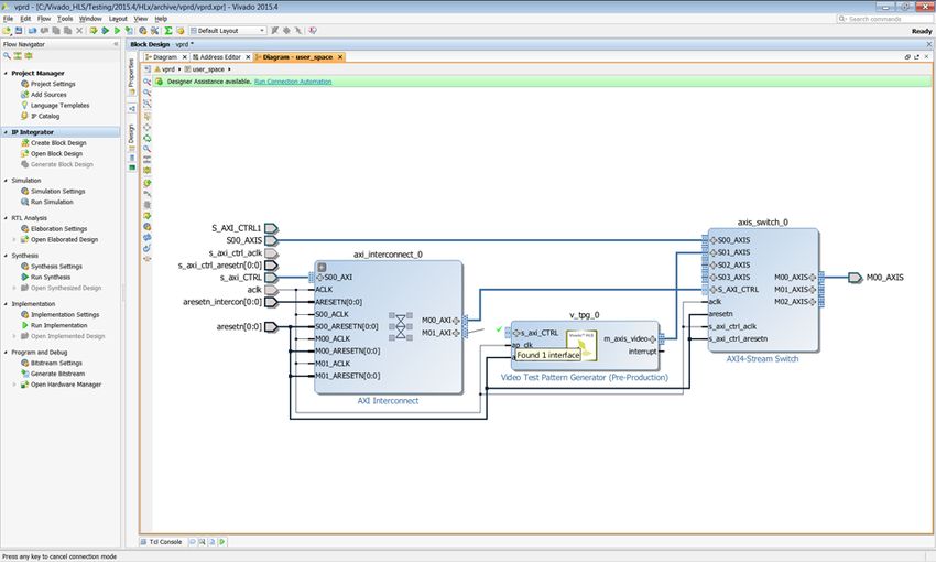
Table of Contents
   Revision History . . . . . . . . . . . . . . . . . . . . . . . . . . . . . . . . . . . . . . . . . . . . . . . . . . . . . . . . . . . . . . . . . . . . 2

Chapter 1: High-Level Productivity Design Methodology
   About This Guide . . . . . . . . . . . . . . . . . . . . . . . . . . . . . . . . . . . . . . . . . . . . . . . . . . . . . . . . . . . . . . . . . . 5
   Need for a New Design Methodology . . . . . . . . . . . . . . . . . . . . . . . . . . . . . . . . . . . . . . . . . . . . . . . . . 6
   Design Process . . . . . . . . . . . . . . . . . . . . . . . . . . . . . . . . . . . . . . . . . . . . . . . . . . . . . . . . . . . . . . . . . . . . 9
   Accessing Documentation and Training . . . . . . . . . . . . . . . . . . . . . . . . . . . . . . . . . . . . . . . . . . . . . . . 10

Chapter 2: System Design
   Overview. . . . . . . . . . . . . . . . . . . . . . . . . . . . . . . . . . . . . . . . . . . . . . . . . . . . . . . . . . . . . . . . . . . . . . . . 12
   System Partitioning . . . . . . . . . . . . . . . . . . . . . . . . . . . . . . . . . . . . . . . . . . . . . . . . . . . . . . . . . . . . . . . 12
   System Development. . . . . . . . . . . . . . . . . . . . . . . . . . . . . . . . . . . . . . . . . . . . . . . . . . . . . . . . . . . . . . 16

Chapter 3: Shell Development
   Overview. . . . . . . . . . . . . . . . . . . . . . . . . . . . . . . . . . . . . . . . . . . . . . . . . . . . . . . . . . . . . . . . . . . . . . . . 23
   Shell Design . . . . . . . . . . . . . . . . . . . . . . . . . . . . . . . . . . . . . . . . . . . . . . . . . . . . . . . . . . . . . . . . . . . . . 24
   Shell Verification . . . . . . . . . . . . . . . . . . . . . . . . . . . . . . . . . . . . . . . . . . . . . . . . . . . . . . . . . . . . . . . . . 26

Chapter 4: C-Based IP Development
   Overview. . . . . . . . . . . . . . . . . . . . . . . . . . . . . . . . . . . . . . . . . . . . . . . . . . . . . . . . . . . . . . . . . . . . . . . .   29
   Fast C Verification . . . . . . . . . . . . . . . . . . . . . . . . . . . . . . . . . . . . . . . . . . . . . . . . . . . . . . . . . . . . . . . .       30
   C Language Support for Synthesis. . . . . . . . . . . . . . . . . . . . . . . . . . . . . . . . . . . . . . . . . . . . . . . . . . . .                   35
   Using Hardware Optimized C Libraries. . . . . . . . . . . . . . . . . . . . . . . . . . . . . . . . . . . . . . . . . . . . . . . .                       39
   Understanding Vivado HLS . . . . . . . . . . . . . . . . . . . . . . . . . . . . . . . . . . . . . . . . . . . . . . . . . . . . . . . . .                39
   Optimization Methodology . . . . . . . . . . . . . . . . . . . . . . . . . . . . . . . . . . . . . . . . . . . . . . . . . . . . . . . . .                45
   Optimization Strategies . . . . . . . . . . . . . . . . . . . . . . . . . . . . . . . . . . . . . . . . . . . . . . . . . . . . . . . . . . . .           55
   RTL Verification . . . . . . . . . . . . . . . . . . . . . . . . . . . . . . . . . . . . . . . . . . . . . . . . . . . . . . . . . . . . . . . . . .      58
   IP Packaging . . . . . . . . . . . . . . . . . . . . . . . . . . . . . . . . . . . . . . . . . . . . . . . . . . . . . . . . . . . . . . . . . . . . .    59
   Design Analysis and Optimization . . . . . . . . . . . . . . . . . . . . . . . . . . . . . . . . . . . . . . . . . . . . . . . . . . .                    59

Chapter 5: System Integration
   Overview. . . . . . . . . . . . . . . . . . . . . . . . . . . . . . . . . . . . . . . . . . . . . . . . . . . . . . . . . . . . . . . . . . . . . . . . 63
   Initial System Integration . . . . . . . . . . . . . . . . . . . . . . . . . . . . . . . . . . . . . . . . . . . . . . . . . . . . . . . . . . 63

UltraFast High-Level Productivity Design Methodology Guide                                                                             Send Feedback
                                                                                                                                                                  3
UG1197 (v2019.2) January 6, 2020            www.xilinx.com
Automated System Integration. . . . . . . . . . . . . . . . . . . . . . . . . . . . . . . . . . . . . . . . . . . . . . . . . . . . . . 66
   Designing for the Future . . . . . . . . . . . . . . . . . . . . . . . . . . . . . . . . . . . . . . . . . . . . . . . . . . . . . . . . . . . 69

Appendix A: Additional Resources and Legal Notices
   Xilinx Resources . . . . . . . . . . . . . . . . . . . . . . . . . . . . . . . . . . . . . . . . . . . . . . . . . . . . . . . . . . . . . . . . . .     72
   Solution Centers. . . . . . . . . . . . . . . . . . . . . . . . . . . . . . . . . . . . . . . . . . . . . . . . . . . . . . . . . . . . . . . . . .      72
   Documentation Navigator and Design Hubs . . . . . . . . . . . . . . . . . . . . . . . . . . . . . . . . . . . . . . . . . . .                            72
   References . . . . . . . . . . . . . . . . . . . . . . . . . . . . . . . . . . . . . . . . . . . . . . . . . . . . . . . . . . . . . . . . . . . . . .   73
   Training Resources. . . . . . . . . . . . . . . . . . . . . . . . . . . . . . . . . . . . . . . . . . . . . . . . . . . . . . . . . . . . . . . .        73
   Please Read: Important Legal Notices . . . . . . . . . . . . . . . . . . . . . . . . . . . . . . . . . . . . . . . . . . . . . . . .                     74

UltraFast High-Level Productivity Design Methodology Guide                                                                            Send Feedback
                                                                                                                                                                 4
UG1197 (v2019.2) January 6, 2020            www.xilinx.com
Chapter 1

High-Level Productivity Design
Methodology

       About This Guide
       Xilinx® programmable devices have capacities of multi-million Logic Cells (LC), and
       integrate an ever-increasing share of today’s complex electronic systems. This High-Level
       Productivity Design Methodology provides a set of best practices to create such complex
       systems within short design cycles.

       The methodology focuses on the following concepts:

       •   Using parallel development flows for the valuable differentiated logic which
           differentiates your products in the marketplace and the shell used to integrate the
           differentiated logic with the rest of the ecosystem.
       •   Extensive use of a C-based IP development flow for the differentiated logic to provide
           simulations that are orders of magnitude faster than RTL simulations, as well as
           accurately timed and optimized RTL.
       •   Use of existing pre-verified, block, and component-level IP to quickly build the shell
           which encapsulates your differentiated logic in the system.
       •   Use of scripts to highly automate the flow from accurate design validation through to
           programmed FPGA.

       The recommendations in this guide have been gathered from a large pool of expert users
       over the past few years. They have consistently delivered the following improvements over
       traditional RTL design methodologies:

       •   4X speed up in development time for designs.
       •   10X speed up in the development time for derivative designs.
       •   0.7X to 1.2X the Quality of Results (QoR).

UltraFast High-Level Productivity Design Methodology Guide                    Send Feedback
                                                                                                    5
UG1197 (v2019.2) January 6, 2020            www.xilinx.com
Chapter 1: High-Level Productivity Design Methodology
Although this guide focuses on large complex designs, the practices discussed are suitable
for, and have successfully been applied in, all types of design including:
• Digital Signal Processing:
° Image processing
° Video
° Radar
• Automotive
• Processor acceleration
• Wireless
• Storage
• Control systems
Need for a New Design Methodology
The advanced designs used in today’s increasingly complex electronic products are
stretching the boundaries of density, performance, and power. They create a challenge for
design teams to hit a target release window within their allocated budget.
A productive methodology for addressing these design challenges is one where more time
is spent at higher levels of abstraction, where verification times are the fastest and
productivity gains are the greatest.
The need for a new design methodology is highlighted in the following figure, where the
area of each region represents the percentage of development effort at each stage of the
design flow.
• With a traditional RTL methodology most of the effort is spent on the implementation
details.
• In a high-level productivity design methodology, most of the effort is spent designing
and verifying if you are building the right system.
UltraFast High-Level Productivity Design Methodology Guide Send Feedback
6
UG1197 (v2019.2) January 6, 2020 www.xilinx.comChapter 1: High-Level Productivity Design Methodology
X-Ref Target - Figure 1-1
Traditional Alogorithmic Design
RTL Methodology Methodology
RTL Platform & IP Reuse
Design C Based IP Design
IP Configuration
Place & Route
IP Integration
Design
Design Closure Closure
;
Figure 1-1: High-Level Productivity Design Methodology Comparison
Traditional Methodology
Traditional design development starts with experienced designers estimating how their
design will be implemented in a new technology, capturing the design in Register Transfer
Levels (RTLs), performing a few trials through synthesis and place and route to confirm their
estimations and then proceeding to capture the remainder of the design. This is done while
typically synthesizing each block in turn to re-confirm that the implementation details are
acceptable.
The primary method for confirming that the design provides the intended functionality is to
simulate the RTL. The detailed bit-accurate and cycle-accurate nature of an RTL description,
although highly accurate, makes this process both slow and error prone.
Only when all blocks in the design have been captured in RTL can a full verification of the
system be performed, often resulting in adjustments to the RTL. After all blocks in the
system have been verified, they can be placed and routed together, and the accuracy of
earlier estimations of timing and area can be either fully confirmed or shown to be
inaccurate. This also often results in changes to the RTL, re-initiating another verification of
the system and another re-implementation.
Designers are now often required to implement hundreds of thousands of lines of RTL code
in a given project and spend much of their design time on implementation details. As
highlighted in Figure 1-1, designers spend considerably more of their time implementing
the design, rather than designing the novel and innovative solutions that all products
require to remain competitive.
Moving to a newer technology to improve performance or a slower technology to provide
more competitive pricing often means the majority of the RTL has to be re-written;
designers must re-implement the amount of logic between the registers.
UltraFast High-Level Productivity Design Methodology Guide Send Feedback
7
UG1197 (v2019.2) January 6, 2020 www.xilinx.comChapter 1: High-Level Productivity Design Methodology
High-Level Productivity Design Methodology
The High-Level Productivity Design Methodology traverses the same basic steps as a more
traditional RTL methodology, as shown in Figure 1-1. However, it allows designers to spend
more time designing value-add solutions. The main attributes of a high productivity
methodology are:
• The concept of a shell that is developed and verified in parallel with the differentiated
logic. This shell encompasses the differentiated logic that captures the I/O peripherals
and interfaces in a separate design project
• Using C-based IP simulation to decrease simulation times by orders of magnitude over
traditional RTL simulation, providing designers the time to design the ideal solution.
• Using the Xilinx Vivado® Design Suite to highly automate the path to timing closure
through the use of C-based IP development, IP re-use and standard interfaces.
° Making use of the Vivado IP Catalog to easily re-use your own block and
component level IP and provide easy access to the Xilinx IP already verified and
known to implement well in the technology.
All steps in the High-Level Productivity Design Methodology can be performed interactively
or using command line scripts. The result of all manual interactions can be saved to scripts,
allowing the entire flow to be fully automated, from the design simulation through to
programming the FPGA. Depending on your design and the runtime of the RTL system level
simulation, this flow makes it possible to generate an FPGA bitstream and test the design
on the board, often before any RTL design simulation has completed.
Even greater productivity improvements come when design derivatives are created.
C-based IP is easily targeted to different devices, technologies, and clock speeds: as easy as
changing a tool option. A fully scripted flow, with automated timing closure through C
synthesis, means derivative designs can be quickly verified and assembled.
UltraFast High-Level Productivity Design Methodology Guide Send Feedback
8
UG1197 (v2019.2) January 6, 2020 www.xilinx.comChapter 1: High-Level Productivity Design Methodology
Design Process
The steps in the design process are shown in the following figure.
X-Ref Target - Figure 1-2
3DUWLWLRQLQJ
Platform Creation & Verification
6\VWHP
C IP Development
System Creation
Platform Design
C IP
System Generator IP
RTL IP
Catalog IP
System Implementation
System Verification
;
;
Figure 1-2: High-Level Productivity Design Flow
After the initial stage of system partitioning, described in Chapter 2, System Design, a key
feature of this design flow is the overlapping nature of the development.
• A Shell Development Flow: Through the use of Vivado IP Integrator and the IP
Catalog, the Vivado Design Suite enables fast, efficient block-level integration. Much of
the critical aspects for system performance, including detail orientated interface
creation, verification, and pin-planning, can be separated into a parallel development
effort and given the focus they require. This flow is described in Chapter 3, Shell
Development.
• C Based IP Development: It takes approximately 1 or 2 days to simulate a full frame of
video using RTL simulation (depending on the design, the host machine, etc.). It takes
approximately 10 seconds to perform the same bit-level accurate simulation using
C/C++. The productivity benefits of a C-based development flow cannot be ignored.
This flow is described in Chapter 4, C-Based IP Development.
• System Creation: Vivado IP integrator and the IP catalog allow C-based IP to be
quickly combined into a system block design using the shell design, legacy RTL IP,
System Generator IP, and Xilinx IP. Automated interface connections and the ability to
script the system creation mean that the system can be generated and re-generated
quickly throughout the IP development process. This flow is described in Chapter 5,
System Integration.
• System Implementation: You can ensure that minimal time is spent on design closure
by using a shell design that is already verified, C-based IP automatically optimized for
UltraFast High-Level Productivity Design Methodology Guide Send Feedback
9
UG1197 (v2019.2) January 6, 2020 www.xilinx.comChapter 1: High-Level Productivity Design Methodology
the device and clock frequency, and existing verified IP, all connected through industry
standard Arm AMBA® AXI4 protocol-compliant interfaces. This flow is launched from
the system block design with a few clicks of the mouse or using a scripted flow. This
flow is described in Chapter 5, System Integration.
• System Verification: This is be performed using gate-level accurate RTL simulations
and/or by programing the FPGA and verifying the design on the board. Because the
RTL simulations are used to verify the system—not the iterative simulations used to
validate the design during development—only a single simulation is required at the
end of the design flow. This flow is described in Chapter 5, System Integration.
Accessing Documentation and Training
Access to the right information at the right time is critical for timely design closure and
overall design success. Reference guides, user guides, tutorials, and videos get you up to
speed as quickly as possible with the Vivado Design Suite. This section lists some of the
sources for documentation and training.
Using the Documentation Navigator
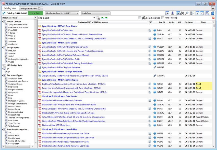
The Vivado Design Suite ships with the Xilinx Documentation Navigator, as shown in
Figure 1-3, which provides an environment to access and manage the entire set of Xilinx
software and hardware documentation, training, and support materials. The Documentation
Navigator allows you to view current and past Xilinx documentation. You can filter the
documentation display based on release, document type, or design task. When coupled
with a search capability, you can quickly find the right information. Methodology Guides
appear as one of the filters under Document Types, which allows you to reach any of
Methodology Guides almost instantaneously.
Xilinx uses the Documentation Navigator to provide you with up-to-date documentation
using the Update Catalog feature. This feature alerts you about available catalog updates
and provides details about the documents that are involved. Xilinx recommends that you
always update the catalog when alerted to keep it current. Additionally, you can establish
and manage local documentation catalogs with specified documents.
The Documentation Navigator has a tab called the Design Hub View. Design hubs are
collections of documentation related by design activity, such as Applying Design
Constraints, Synthesis, Implementation, and Programming and Debug. Documents and
videos are organized in each hub in order to simplify the learning curve for that area. Each
hub contains sections such as Getting Started, Support Resources (with an FAQ for that
flow), and Additional Learning Materials. For new users, the Getting Started section
provides a good place to start. For those already familiar with the flow, Key Concepts and
the FAQ may be of particular interest to gain expertise with the Vivado Design Suite.
UltraFast High-Level Productivity Design Methodology Guide Send Feedback
10
UG1197 (v2019.2) January 6, 2020 www.xilinx.comChapter 1: High-Level Productivity Design Methodology
X-Ref Target - Figure 1-3
Figure 1-3: Xilinx Documentation Navigator
UltraFast High-Level Productivity Design Methodology Guide Send Feedback
11
UG1197 (v2019.2) January 6, 2020 www.xilinx.comChapter 2
System Design
Overview
Before starting on your project, it is important to have a clear understanding of how you will
design and assemble your system. In any complex system, there are multiple paths to a
solution. These paths are dictated by the various choices you make on what IP blocks to
create from scratch, what IP you can re-use, and the tools and methodology used to
validate the IP, integrate the IP in a system, and verify the system.
This chapter addresses the system partitioning choices you will make and reviews key
features of the Vivado ® Design Suite which help automate the process of system
development.
• System Partitioning
• System Development
System Partitioning
In a typical design, the logic on the periphery of the design is dedicated to interfacing with
external devices, typically using standard interfaces. Example of this are DDR, Gigabit
Ethernet, PCIe, HDMI, ADC/DAC, and Aurora interfaces. These interfaces and the
components used to implement them are typically standard to multiple FPGA designs
within the same company.
In the High-Level Productivity Design Methodology this logic is separated from the
differentiated logic and is considered the shell. The figure below shows an example shell
block design. The shaded area in the center of the figure below indicates where the
differentiated logic or shell verification IP can be added.
UltraFast High-Level Productivity Design Methodology Guide Send Feedback
12
UG1197 (v2019.2) January 6, 2020 www.xilinx.comChapter 2: System Design
X-Ref Target - Figure 2-1
RS232
Tx Unit
AXI Memory I/F DDR
Interconnect Generator
Output
AXI
HDMI
DMA Engine Interconnect
Tx
Timing
Controller
Differentiated
Logic AXI Stream
to Video
nput Video To
HDMI
AXI-
Rx
Stream
Shell
X23582-120
Figure 2-1: Shell Design Example
Key benefits of this methodology are:
• The shell is developed and verified independently of the rest of the design.
• Board-level integration and device pin planning are addressed by a separate dedicated
team working in parallel.
• The shell is saved and re-used (even re-edited), allowing multiple derivative designs to
be quickly realized.
• The differentiated logic is developed and verified independently of the shell.
• The pre-verified shell and differentiated logic are quickly integrated into a complete
system.
When partitioning your system, the first task is to determine what will be implemented in
the shell and what will be implemented as differentiated logic.
Shell Design
A shell design provides two key attributes to a high productivity methodology:
• Separating standard interface logic from the differentiated logic, allowing the
development and verification of both to proceed in parallel.
UltraFast High-Level Productivity Design Methodology Guide Send Feedback
13
UG1197 (v2019.2) January 6, 2020 www.xilinx.comChapter 2: System Design
• Creating a re-usable design, or shell, that can be used to quickly create design
derivatives. A shell should ideally contain the parts of the design that are standard,
such as design interfaces and interface IP. However, a shell can also contain blocks used
for pre-processing or post-processing. If the processing functions are independent of
the core design IP, and if the processing functions could be used across multiple
designs, it is more ideal to place these blocks in the shell. The shell re-use
methodology allows blocks to be easily removed from the shell.
Irrespective of the logic you decide to incorporate into the shell design, a key attribute of
the shell design is that the internal interfaces, those which connect to the internal design IP,
should be implemented using standard interfaces. Use of standard internal interfaces such
as AXI will enhance the shell re-use by doing the following:
• Allowing the shell to be easily connected to a design IP that has yet to be developed
• Ensuring that verification of the shell also verifies the internal interfaces
• Enabling use of the high productivity integration features described in IP Integrator
and Standard Interfaces
Even if you are initially only thinking of one design, a shell based methodology allows you
to easily create derivative designs after the initial design is implemented.
More details about shell development and verification are described in Chapter 3, Shell
Development.
IP Design
The key feature of the IP development flow is that it includes only the IP that differentiates
the product from the shell.
The design IP is not standard and will be developed. Much of the development effort is
running simulations to validate that the design provides the correct functionality. This effort
can be minimized, and simulation run times improved, by not including standard blocks
that do not impact the new functionality being developed; those blocks should be in the
shell.
The figure below shows a representation of a complete system with design IP added to the
shell design. A key feature of the completed system is that it might contain IP developed
from many different sources, such as:
• IP generated from C/C++ using Vivado HLS
• IP generated from System Generator
• IP from RTL
• Xilinx ® IP
• Third-Party IP
UltraFast High-Level Productivity Design Methodology Guide Send Feedback
14
UG1197 (v2019.2) January 6, 2020 www.xilinx.comChapter 2: System Design
X-Ref Target - Figure 2-2
RS232
Design IP
DDR
U67
U5 U7 Output
U6
Sys C
Gen Based
IP IP
U123 C
Based
U1 U2 U3 IP
C C C
RTL Xilinx
Based Based Based
IP IP
IP IP IP
U4 U8
Input
Platform IP
X23583-120619
Figure 2-2: System Design Example
In a high productivity design methodology, one of the greatest benefits comes from the
verification speed of C simulation. From a design creation perspective, there is large
productivity gain by simulating the C blocks together during development.
• Fast C simulation allows the designer to quickly develop and verify an accurate
solution.
• Multiple C blocks simulated together help each verify the output of the other.
• A larger overall productivity benefit can be achieved if several C IP are combined
together in a C simulation.
The figure above, Figure 2-2, highlights a dilemma you may face when using C IP. Blocks U1,
U2, and U3 are all C IP and could be grouped into a single top-level U123. Similarly, blocks
U6 and U7 could be grouped into a single IP block, U67. You can do one of the following:
• Create multiple smaller C IP blocks, such as U1, U2, U3, U6 and U7.
• Create a few large C IP blocks, such as U123 and U67 outlined in the figure above.
From a design integration perspective, there is no difference between these methods; if the
IP blocks are generated with AXI interfaces, they are easily integrated together using IP
integrator. For designers who are new to C-based IP development, it might make more
sense to work on smaller blocks, learn how to optimize each small block independently, and
then integrate multiple smaller IPs together. For designers who are comfortable with C IP
development, it might make more sense to generate a few large C IP blocks.
UltraFast High-Level Productivity Design Methodology Guide Send Feedback
15
UG1197 (v2019.2) January 6, 2020 www.xilinx.comChapter 2: System Design
IMPORTANT: The key productivity benefit is being able to simulate as many C IP blocks as one C
simulation during development.
In the situation described above, the same C test bench that verifies blocks U1, U2, and U3
would be used to verify U123. The difference in IP generation is that you either set the top
level for C synthesis in Vivado HLS as function U123, or as function U1 followed by U2 and
U3.
Regardless of which route is taken to create the IP blocks, each of the IP blocks should be
verified in isolation as follows:
• IP developed from C/C++ is verified using the C/RTL co-simulation feature of Vivado
HLS, allowing the RTL to be verified using the same C test bench used to verify the C
based IP.
• IP developed from System Generator is verified using the MathWorks Simulink design
environment provided in System Generator. The Simulink environment enables the easy
generation of complex input stimuli and analysis of complex results through the use of
pre-defined simulation elements. IP generated from C/C++ and through traditional RTL
can be imported into the System Generator environment to take advantage of this
verification.
• For IP generated from RTL, you must create an RTL test bench to verify the IP.
• IP provided by Xilinx and third-party providers is pre-verified, however you might wish
to create a test bench to confirm its operation based on your own set of configuration
parameters.
The use of standard AXI interfaces on the IP allows the IP to be quickly integrated, both with
each other and with the shell design.
System Development
Although the concept of using a shell and multiple IP blocks is not new to FGPA designers,
this methodology typically requires lots of RTL to be developed and simulated, requiring
stitching hundreds, if not thousands, of individual RTL signals together multiple times to
make the following connections:
• The shell to verification IP
• The shell to the core design IP
• The shell to derivative core design IP.
In lieu of the many additional man-hours in both design and verification effort it would take
to use this methodology in a traditional RTL design flow (this is an error prone task when
UltraFast High-Level Productivity Design Methodology Guide Send Feedback
16
UG1197 (v2019.2) January 6, 2020 www.xilinx.comChapter 2: System Design
performed in a text editor), design teams typically design and integrate everything
together.
Vivado IP integrator enables this methodology and allows IPs to be quickly integrated
without the traditional hand-editing of RTL files.
The key features for using this methodology are:
• Vivado IP Catalog
• IP integrator and standard interfaces
Vivado IP Catalog
The Vivado IP Catalog is the backbone of any methodology that uses IP and IP re-use.
Figure 2-3 shows an alternative view of the design process for the High-Level Productivity
Design Methodology highlighting where and when the IP Catalog is used.
IMPORTANT: Use of the IP Catalog is key to enabling a High-Level Productivity Design Methodology.
X-Ref Target - Figure 2-3
3DUWLWLRQLQJ
Shell Creation & Verification
6\VWHP
Custom Logic Development
System Creation
System Implementation
System Verification
RTL IP System Generator
IP Partner IP Vivado IP Catalog (Xilinx IP built-in)
;
Figure 2-3: IP Catalog and the Design Process
The IP Catalog has the following features:
• Includes approximately 200 IPs from Xilinx. For more information, refer to the Xilinx
Intellectual Property Page [Ref 12].
• Saves the output from C based IP development.
• Can be enhanced with System Generator, legacy RTL, and Xilinx Partner IP.
• Contains a large number of interface IPs, supports the use of legacy RTL IP, and is used
extensively when creating the shell.
• Is the source for all IP blocks during system integration.
UltraFast High-Level Productivity Design Methodology Guide Send Feedback
17
UG1197 (v2019.2) January 6, 2020 www.xilinx.comChapter 2: System Design
• Provides the RTL implementations used during system integration and verification.
During shell development, the shell is assembled in IP integrator using IP from the IP
Catalog. This might include interface IP provided by Xilinx (Ethernet, VGA, CPRI, Serial
Transceivers, etc.), IP from Xilinx partners, legacy RTL package as IP for the IP Catalog, or IP
created by Vivado HLS and System Generator.
Details about packaging legacy RTL as IP are provided in the Vivado Design Suite Tutorial:
Creating and Packaging Custom IP (UG1119) [Ref 5].
Details on creating IP with AXI interfaces from System Generator are provided in the Vivado
Design Suite User Guide: Model-Based DSP Design Using System Generator (UG897) [Ref 6].
The default output from Vivado HLS is an IP packaged for the IP Catalog. This is described
in IP Packaging.
IP Integrator and Standard Interfaces
The Vivado IP integrator allows IP blocks to be quickly added to a canvas and connected,
and is a key enabler of a high productivity design methodology.
IMPORTANT: The key to high productivity using Vivado IP integrator is the use of standard interfaces.
Figure 2-4 shows an example block design captured in IP integrator.
UltraFast High-Level Productivity Design Methodology Guide Send Feedback
18
UG1197 (v2019.2) January 6, 2020 www.xilinx.comChapter 2: System Design
X-Ref Target - Figure 2-4
Figure 2-4: IP Integrator Block Design
The connection types include:
• Pin-level connections such as clock and reset signals.
• Bus-level connections such as AXI, AXI4-Lite and AXI4-Stream buses.
• Board-level connections such as DDR.
Connections in IP integrator are made by using the mouse to graphically connect the pins
on each IP together. In addition to supporting basic connecting bit-level connections,
support is provided for bus-level connection and designer assistance.
UltraFast High-Level Productivity Design Methodology Guide Send Feedback
19
UG1197 (v2019.2) January 6, 2020 www.xilinx.comChapter 2: System Design
The following figure highlights the advantage of bus-level connections. In this example, two
AXI master interfaces are to be connected together. Note that as soon as the connection is
made to the first port, all possible valid connections are identified on the diagram by green
check marks.
IMPORTANT: IP integrator does not allow illegal connections to be made. This eliminates the types of
connectivity errors typically made when this process is performed through manual edits.
X-Ref Target - Figure 2-5
Figure 2-5: Connection Automation
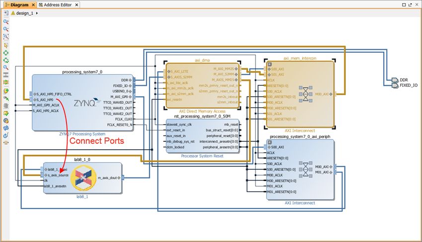
A further productivity feature provided by the use of standard AXI interfaces and IP
integrator is the automatic generation of the AXI interconnect IP. Figure 2-6 shows the
result when connecting:
• An AXI output on one block
• An AXI4-Stream input on another block
IP integrator automatically adds the AXI Interconnect IP to connect the master type
interface to a stream type interface.
UltraFast High-Level Productivity Design Methodology Guide Send Feedback
20
UG1197 (v2019.2) January 6, 2020 www.xilinx.comChapter 2: System Design
X-Ref Target - Figure 2-6
Figure 2-6: Automated AXI Interconnect IP
This AXI Interconnect IP is provided in the IP Catalog and can be added manually but IP
integrator automates the task. Furthermore, if the final block design is saved as a script, the
Tcl commands simply state which pins to connect.
TIP: When you upgrade to a new release of the Vivado Design Suite and Xilinx IP, re-run the script to
make sure that it uses the latest interconnect logic.
A final case for using standard interfaces in your designs is the designer assistance
provided for board level connections. In addition to allowing the target device to be
selected, the Vivado Design Suite allows selection of target boards. IP integrator is
board-aware and is able to automate board-level connections.
After confirmation from the designer, IP integrator automatically makes the connections
between the IP and FPGA pins (board connections).
UltraFast High-Level Productivity Design Methodology Guide Send Feedback
21
UG1197 (v2019.2) January 6, 2020 www.xilinx.comChapter 2: System Design
X-Ref Target - Figure 2-7
Figure 2-7: Block Automation
IP integrator automates integration of IP into a block level diagram. Additional features
include Design Rule Checks using the Validate feature and the automatic addition of clock
and reset logic for AXI Interconnect IP. The key to taking advantage of this automation, and
enabling a productive shell methodology, is the use of standard interfaces and AXI
interfaces for on-chip communication.
UltraFast High-Level Productivity Design Methodology Guide Send Feedback
22
UG1197 (v2019.2) January 6, 2020 www.xilinx.comChapter 3
Shell Development
Overview
The use of a shell is a critical part of the productivity benefits provided by a high
productivity design methodology. A shell design contains all of the standard interfaces and
processing blocks that provide the connection between the core design IP and the
remainder of the system, and is developed in parallel to the core design IP.
A methodology that incorporates shell design provides key productivity gains, such as:
• It allows the development of the design interfaces and I/O planning to proceed
independently of the core design.
• It enables the verification of the design interfaces to start before the core design IP is
ready.
• It reduces the verification time for the interfaces because the design is smaller; it does
not contain the core design IP that typically represents the majority of the logic in the
system.
• It promotes a highly productive design re-use methodology, allowing derivative
designs to be easily created.
An overview of the shell design methodology is shown in Figure 3-1. A key attribute of the
methodology is the re-use of the shell design.
UltraFast High-Level Productivity Design Methodology Guide Send Feedback
23
UG1197 (v2019.2) January 6, 2020 www.xilinx.comChapter 3: Shell Development
X-Ref Target - Figure 3-1
Create Vivado Project
Develop Shell Block
Diagram
Save Project
Verify the Design FPGA
Open Project Add Verification IP
Interfaces Bitstream
FPGA
Open Project System Creation, Implementation and Verification
Bitstream
FPGA
Open Project Derivative design (creation, implementation & verification)
Bitstream
;
Figure 3-1: Shell Methodology
Shell development consists of two equally important processes: shell design and shell
verification.
Shell Design
A shell design consists only of the design periphery, as shown in the figure above, and must
be in a form that makes the design easy to re-use. The shell will be saved and re-opened to
form the basis of multiple projects.
To achieve the level of design re-use required to enable the flow shown in the above figure,
the shell design should be captured as a block design in IP integrator that can be easily
saved and re-opened to form the basis of other design projects.
Assemble Existing IP
A shell design is assembled as block design in IP integrator using IP from the IP Catalog.
IMPORTANT: In preparation for creating your shell, package any existing RTL or company-specific IP
you want to use in the shell design as IP for use in the IP Catalog. This allows you to add the IP in the
shell block design.
For details about how to package blocks for the IP Catalog, refer to the Vivado ® Design
Suite Tutorial: Creating and Packaging Custom IP (UG1119) [Ref 5].
UltraFast High-Level Productivity Design Methodology Guide Send Feedback
24
UG1197 (v2019.2) January 6, 2020 www.xilinx.comChapter 3: Shell Development
Shell Design Project
After you assemble your IP, create a Vivado RTL project.
TRAINING: Creating a Vivado RTL project is detailed in the Vivado Design Suite QuickTake Video:
Creating Different Types of Projects.
When creating the Vivado project:
• Specify the project as an RTL project and select Do not specify any sources at this
time. The sources for the shell design are the IP you have packaged in the IP Catalog.
• Ideally, select the target as a Xilinx ® board. The I/O for devices used on Xilinx boards
has already been configured. This allows you to get started in the quickest possible
time—while your own custom board is developed—and allows you to use Designer
Automation within IP integrator for I/O connections.
If you do not specify a Xilinx board as the target, you will also need to specify the I/O
connections for the target device. Refer to this link in the UltraFast Design Methodology
Guide for the Vivado Design Suite (UG949) [Ref 7].
If you are using your own custom board during the development process, you might want
to create a board file that details the board connections and allows designer automation
within IP integrator, greatly simplifying board level connections. Details on the board file
are provided in “Using the Vivado Design Suite Board Flow,” provided at this link in the
Vivado Design Suite User Guide: System-Level Design Entry (UG895) [Ref 9].
After the project has been created, use the Create Block Design button in the Flow
Navigator to open IP integrator and create a new Block Design. In the IP integrator window,
specify the source of your IP repository and use the Add IP button to start assembling the
shell.
Once the shell is complete, the write_bd_tcl command is used to save the entire block
design as a Tcl script. This script contains everything that is needed to re-generate the block
design from scratch. The block design and Vivado project are saved and ready for the next
stages of verification and system development.
In depth information on pin planning, IP integrator, and other features in the Vivado Design
Suite is provided in the Design Hubs tab of the Documentation Navigator. For more
information, refer to Using the Documentation Navigator.
UltraFast High-Level Productivity Design Methodology Guide Send Feedback
25
UG1197 (v2019.2) January 6, 2020 www.xilinx.comChapter 3: Shell Development
Shell Verification
After the shell design is created, shell verification can proceed. In the verification process,
the shell design is re-opened and verification IP is added to the design to confirm that the
interfaces are working.
Shell Verification Projects
The first step in verifying the shell design is to create a new verification project using one
of the following two options.
• Open the Vivado project for the shell design and use File > Save Project As to save the
shell design in a new project.
• Create a new Vivado RTL project (with no RTL sources) and the same target device or
board. Then select Create Block Design, and in the console, source the Tcl script saved
using write_bd_tcl to regenerate the shell Block Design in the new project.
Multiple verification projects might be required to ensure that the complexity of the
verification design is manageable. The figure below shows an example shell verification
design. This example tests only a single interface.
UltraFast High-Level Productivity Design Methodology Guide Send Feedback
26
UG1197 (v2019.2) January 6, 2020 www.xilinx.comChapter 3: Shell Development
X-Ref Target - Figure 3-2
C Test Bench
main()
generate() validate()
process()
readIO() procIO() compare() write_IO()
queue() data_proc()
morph()
align() interp() margin()
Design Function
The synthesis top-level is process()
X23584-120619
Figure 3-2: Shell Verification Example
Verification IP
Verification IP is added to the shell design from the Vivado IP Catalog to verify the design.
The verification IP can be developed using any of the techniques discussed in this guide:
RTL, System Generator, or C-based IP. The following examples shows how if standard AXI
Interface IPs are used, a small C file can be used to quickly create, for example, a HANN
window of N samples output on an AXI4-Stream interface. An AXI memory mapped
interface can be implemented by simply changing the interface directive to m_axi from
axis, as shown in the following code example:
void verify_IP_Hann(float outdata[WIN_LEN]) {
// Specify AXI4-Stream output
#pragma HLS INTERFACE axis port=outdata
// Alternative output AXI4M (commented out)
//#pragma HLS INTERFACE m_axi port=outdata
float coeff[WIN_LEN];
coeff_loop:for (int i = 0; i < WIN_LEN; i++) {
coeff[i] = 0.5 * (1.0 - cos(2.0 * M_PI * i / WIN_LEN));
}
UltraFast High-Level Productivity Design Methodology Guide Send Feedback
27
UG1197 (v2019.2) January 6, 2020 www.xilinx.comChapter 3: Shell Development
winfn_loop:for (unsigned i = 0; i < WIN_LEN; i++) {
outdata[i] = coeff[i];
}
}
For information about how to use Vivado HLS to create interface blocks between other IPs,
refer to Methods for Integrating AXI4-based IP Using Vivado IP Integrator Application Note
(XAPP1204) [Ref 10].
Verifying the Shell
If a top-level test bench is added to the simulation sources, the shell design can be verified
by simulation prior to programming the FPGA.
Verification of the shell using RTL simulation requires the creation of the RTL test bench.
This same test bench is used to verify the fully integrated design. If multiple verification
projects are used to verify the shell, the same test bench should be expanded to verify all of
the interfaces.
To verify detailed interfaces on the FPGA, additional signal level debug probes can be
added to the design.
When working in the Block Design, the right-click menu allows nets to be easily marked for
debug. Signals marked for debug can be analyzed during hardware operation: ILA cores are
added to the design to allow the signals to be captured and scanned out of the FPGA for
analysis. Refer to this link in the Vivado Design Suite User Guide: Designing IP Subsystems
Using IP Integrator (UG994) [Ref 8].
The final design is then processed through the Vivado design flow to bitstream. When the
shell is fully verified, any modifications to the shell design, other than modifications to the
verification IP, should be propagated back to the original source shell design project. The
shell design is then ready for the integration of the core design IP.
UltraFast High-Level Productivity Design Methodology Guide Send Feedback
28
UG1197 (v2019.2) January 6, 2020 www.xilinx.comChapter 4
C-Based IP Development
Overview
In a high productivity design flow, the primary means of generating the core design IP is
through the use of C-based IP and High-Level Synthesis (HLS) of C code into RTL. A C-based
IP development flow provides the following benefits:
• Superior simulation speeds provided by C verification
• Automated generation of accurately timed optimized RTL
• Ability to use existing C IP from libraries
• Ease of integrating the resulting RTL IP into a complete system using IP Integrator
This chapter discusses how C-Based IP is created, validated, synthesized, analyzed,
optimized, and packaged into IP for the IP Catalog. The means for achieving this is Vivado ®
High-Level Synthesis (HLS), a tool provided as part of the Vivado Design Suite.
The design flow for Vivado HLS is shown in the figure below. The design flow steps are:
1. Compile, execute (simulate), and debug the C algorithm.
Note: In high-level synthesis, running the compiled C program is referred to as C simulation.
Executing the C program simulates the function to validate that the algorithm is functionally
correct.
2. Synthesize the C program into an RTL implementation, optionally using user
optimization directives.
3. Generate comprehensive reports and analyze the design.
4. Verify the RTL implementation using a push button flow.
5. Package the RTL implementation into a selection of IP formats.
UltraFast High-Level Productivity Design Methodology Guide Send Feedback
29
UG1197 (v2019.2) January 6, 2020 www.xilinx.comChapter 4: C-Based IP Development
X-Ref Target - Figure 4-1
7HVW && &RQVWUDLQWV
%HQFK 6\VWHP& 'LUHFWLYHV
2SHQ&/$3,&
&6LPXODWLRQ &6\QWKHVLV
57/ 9LYDGR+/6 9+'/
$GDSWHU 9HULORJ
57/6LPXODWLRQ 3DFNDJHG,3
9LYDGR
6\VWHP
'HVLJQ
*HQHUDWRU
6XLWH
;
Figure 4-1: Vivado HLS Design Flow
Details about using Vivado HLS are provided in the Vivado Design Suite User Guide:
High-Level Synthesis (UG902) [Ref 2]. This chapter explains a methodology for using Vivado
HLS in a highly productive manner.
Fast C Verification
Simulating an algorithm in C can be orders of magnitude faster than simulating the same
algorithm in RTL.
For example, consider a standard video algorithm. A typical video algorithm in C processes
a complete frame of video data and compares the output image against a reference image
to confirm that the results are correct. The C simulation for this typically takes 10-20
seconds. A simulation of the RTL implementation typically takes a few hours to day(s)
depending on the number of frames and the complexity of the design.
UltraFast High-Level Productivity Design Methodology Guide Send Feedback
30
UG1197 (v2019.2) January 6, 2020 www.xilinx.comChapter 4: C-Based IP Development
The more development performed at the C level, using the simulation speed of software,
the more productive you will be. It is at this level that designers actually design: adjusting
their algorithm, data types, and bit-width to validate and confirm that the design is correct.
The remainder of the flow is development: using a tool chain to implement the correct
design in an FPGA. The benefits provided by the Vivado Design Suite and a High-Level
Productivity Design methodology is the high degree of automation provided to the
development flow.
After the initial FPGA design is implemented, it is not uncommon to create an entire new
bitstream to program the FPGA, using the scripted flow presented in Chapter 5, System
Integration, in less time than it takes to perform a system-wide RTL simulation.
To maximize the productivity of a C-based IP flow, the following should be understood:
• C Test Bench
• Self-Checking Test Bench
• Bit Accurate Data Types
C Test Bench
The top level of every C program is the main() function. Vivado HLS synthesizes any single
function below the level of main(). The function to be synthesized by Vivado HLS is
referred to as the Design Function. This is highlighted in Figure 4-2.
• All functions below the Design Function are synthesized by Vivado HLS.
• Everything outside of the Design Function hierarchy is referred to as the C test bench.
The C test bench includes all of the C code below main() that supplies input data to the
Design Function and accepts output data from the Design Function to confirm that it is
accurate.
UltraFast High-Level Productivity Design Methodology Guide Send Feedback
31
UG1197 (v2019.2) January 6, 2020 www.xilinx.comChapter 4: C-Based IP Development
X-Ref Target - Figure 4-2
RS232
Tx Unit
AXI Memory I/F DDR
Interconnect Generator
Output
AXI
HDMI
DMA Engine Interconnect
Tx
Timing
Controller
Test Pattern
Generator
AXI AXI Stream
Switch to Video
Input Video To
HDMI
AXI-
Rx
Stream
Verification IP Platform IP
X23585-120619
Figure 4-2: C Test Bench
The single biggest mistake made by users new to the Vivado HLS design flow is to proceed
to synthesize their C code without using a C test bench and performing C simulation. This
can be highlighted by the following code. What is wrong with this example of nested loops?
UltraFast High-Level Productivity Design Methodology Guide Send Feedback
32
UG1197 (v2019.2) January 6, 2020 www.xilinx.comChapter 4: C-Based IP Development
#include "Nested_Loops.h"
void Nested_Loops(din_t A[N], dout_t B[N]) {
int i,j;
dint_t acc;
LOOP_I:for(i=0; i < 20; i++){
LOOP_J: for(j=0; j < 20; j++){
if(j=0) acc = 0;
acc += A[i] * j;
if(j=19) B[i] = acc / 20;
}
}
}
This code fails to synthesize into the expected result because the conditional statements
evaluate as FALSE and J is set to 19 at the end of the first iteration of LOOP_J. The
conditional statements should be j==0 and j==19 (using == instead of =). The preceding
code example compiles, executes, and can be synthesized without any issue. However, it will
not do what is expected by a cursory visual evaluation of the code.
In an era where developers consistently use one or more of C/C++, Perl, Tcl, Python, Verilog,
and VHDL on a daily basis, it is hard to catch such trivial mistakes, more difficult still to
catch functional mistakes, and extremely difficult and time consuming to uncover either
after synthesis.
A C test bench is nothing more than a program that calls the C function to be synthesized,
provides it test data, and tests the correctness of its output; this can be complied and run
prior to synthesis and the expected results validated before synthesis.
You might initially feel that you are saving time by going directly to synthesis, but the
benefits of using a C test bench in your design methodology are worth a lot more than the
time it takes to create one.
Self-Checking Test Bench
The Vivado HLS supports C simulation prior to synthesis to validate the C algorithm and
C/RTL co-simulation after synthesis to verify the RTL implementation. In both cases, Vivado
HLS uses the return value of function main() to confirm that the results are correct. An
ideal C test bench has the result checking attributes shown in the code example below. The
outputs from the function for synthesis are saved into the file results.dat and compared
to the correct and expected results, which are referred to as the “golden” results in this
example.
int main () {
...
int retval=0;
fp=fopen("result.dat","w");
...
// Call the function for synthesis
loop_perfect(A,B);
UltraFast High-Level Productivity Design Methodology Guide Send Feedback
33
UG1197 (v2019.2) January 6, 2020 www.xilinx.comChapter 4: C-Based IP Development
// Save the output results
for(i=0; iChapter 4: C-Based IP Development
Bit Accurate Data Types
Arbitrary precision data types are provided with Vivado HLS and allow variables to be
specified at any width. For example, variables might be defined as 12-bit, 22-bit, or 34-bits
wide. Using standard C data types, these variables are required to be 16-bit, 32-bit, and
64-bit, respectively. Using the standard C data types often results in unnecessary hardware
to implement the required accuracy; for example, 64-bit hardware when only 34-bit is
required.
An even greater benefit of using arbitrary precision data types is that the C algorithm can
be simulated using these new bit-widths and the bit-accurate results analyzed. For example,
you might wish to design a filter with 10-bit inputs and 14-bit output and you might
determine that the design can use a 24-bit accumulator. Performing C simulation—which
can simulate the filter with tens of thousands of samples in a matter of minutes—will
quickly confirm whether the signal-to-noise ratio of the output is acceptable. You will
quickly be able to determine if the accumulator is too small or verify that using a smaller,
more efficient accumulator still provides the required accuracy.
IMPORTANT: Simulation of a bit-accurate C is the fastest way to verify your design.
A productive methodology is to start your initial design with standard C data types and
confirm the algorithm performs as designed. Then migrate your C code to use arbitrary
precision data types. This migration to more hardware efficient data types can only be
performed safely and productively if there is a C test bench checking the results, allowing
you to quickly verify the smaller more efficient data types are adequate. Once you are
comfortable with arbitrary precision types, you will typically use arbitrary precision data
types right from the start of your new C project.
The benefits of using a C test bench, and the loss of productivity in not using one as part of
your design methodology, cannot be overstated.
The Vivado HLS examples described at this link in the Vivado Design Suite User Guide:
High-Level Synthesis (UG902) [Ref 2] are all provided with a C, C++, or SystemC test bench.
These examples can be copied and modified to create a C test bench. They include C
functions using arbitrary precision data types.
C Language Support for Synthesis
Understanding what is supported for synthesis is important part of the Vivado HLS
UltraFast design methodology. Vivado HLS provides comprehensive support for C, C++,
and SystemC. Everything is supported for C simulation; however, it is not possible to
synthesize every description into an equivalent RTL implementation.
UltraFast High-Level Productivity Design Methodology Guide Send Feedback
35
UG1197 (v2019.2) January 6, 2020 www.xilinx.comChapter 4: C-Based IP Development
The two key principles to keep in mind when reviewing the code for implementation in an
FPGA are:
• An FPGA is a fixed size resource. The functionality must be fixed at compile time.
Objects in hardware cannot be dynamically created and destroyed.
• All communication with the FPGA must be performed through the input and output
ports. There is no underlying Operating System (OS) or OS resources in an FPGA.
Unsupported Constructs
System Calls
System calls are not supported for synthesis. These calls are used to interact with the OS
upon which the C program executes. In an FPGA there is no underlying OS to communicate
with. Example of systemcalls are time() and printf().
Some commonly used functions are automatically ignored by Vivado HLS and there is no
requirement to remove them from the code. These functions are:
• abort()
• atexit()
• exit()
• fprintf()
• printf()
• perror()
• putchar()
• puts()
An alternative to removing any unsupported code is to guard it from synthesis. The
__SYNTHESIS__ macro is automatically defined by Vivado HLS when synthesis is
performed.
This macro can be used to include code when C simulation is run, but exclude the code
when synthesis is performed.
UltraFast High-Level Productivity Design Methodology Guide Send Feedback
36
UG1197 (v2019.2) January 6, 2020 www.xilinx.comChapter 4: C-Based IP Development
#ifndef __SYNTHESIS__
// The following code is ignored for synthesis
FILE *fp1;
char filename[255];
sprintf(filename,Out_apb_%03d.dat,apb);
fp1=fopen(filename,w);
fprintf(fp1, %d \n, apb);
fclose(fp1);
#endif
Note: Only use the __SYNTHESIS__ macro in the code to be synthesized. Do not use this macro in
the test bench, because it is not obeyed by C simulation or C RTL co-simulation.
If information is required from the OS, the data must be passed into the top-level function
for synthesis as an argument. It is then the task of the remaining system to provide this
information to the synthesized IP block. This can typically be done by implementing the
data port as an AXI4-Lite interface connected to a CPU.
Dynamic Objects
Dynamic objects cannot be synthesized. The function calls malloc(), alloc(),
pre-processor free(), and C++ new and delete dynamically create or destroy memory
resources that exist in the OS memory map. The only memory resources available in an
FPGA are block RAMs and registers. Block RAMs are created when arrays are synthesized
and the values in the arrays must be maintained over one or more clock cycles. Registers are
created when the value stored by a variable must be maintained over one or more clock
cycles. Arrays of a fixed size or variables must be used in place of any dynamic memory
allocation.
As with restrictions on dynamic memory usage, Vivado HLS does not support (for synthesis)
C++ objects that are dynamically created or destroyed. This includes dynamic
polymorphism and dynamic virtual function calls. New functions, which would result in new
hardware, cannot be dynamically created at run time.
For similar reasons, recursion is not supported for synthesis. All objects must be of a known
size at compile time. Limited support for recursion is provided when using templates.
Except for standard data types, such as std::complex, C++ Standard Template Libraries
(STLs) are not supported for synthesis. These libraries contain functions which make
extensive use of dynamic memory allocation and recursion.
SystemC Constructs
An SC_MODULE cannot be nested inside, or derived from, another SC_MODULE.
The SC_THREAD construct is not supported (however, SC_CTHREAD is).
UltraFast High-Level Productivity Design Methodology Guide Send Feedback
37
UG1197 (v2019.2) January 6, 2020 www.xilinx.comChapter 4: C-Based IP Development
Constructs with Limited Support
Top-Level Function
Templates are supported for synthesis but are not supported for use on the top-level
function.
A C++ class object cannot be the top-level for synthesis. The class must be instantiated into
a top-level function.
Pointers to pointers are supported for synthesis but not when used as an argument to the
top-level function.
Pointer Support
Vivado HLS supports pointer casting between native C types but does not support general
pointer casting, such as casting between pointers to differing structure types.
Vivado HLS supports pointer arrays, provided that each pointer points to a scalar or an
array of scalars. Arrays of pointers cannot point to additional pointers.
Recursion
Recursion in an FPGA is only supported through the use of templates. The key to
performing recursion in synthesis is the use of a termination class, with a size of one, to
implement the final call in the recursion.
Memory Functions
The memcpy() and memset() are both supported with the limitation that const values
must be used.
• memcpy(): used for bus burst operation or array initialization with const values. The
memcpy function can only be used to copy values to or from arguments to the
top-level function.
• memset(): used for aggregate initialization with constant set value.
Any code which is not supported for synthesis, or for which only limited support is
provided, must be modified before it can be synthesized.
More complete details on language support and are provided at this link in the Vivado
Design Suite User Guide: High-Level Synthesis (UG902) [Ref 2].
UltraFast High-Level Productivity Design Methodology Guide Send Feedback
38
UG1197 (v2019.2) January 6, 2020 www.xilinx.comYou can also read