AXI High Bandwidth Memory Controller v1.0 - LogiCORE IP Product Guide Vivado Design Suite - Xilinx
←
→
Page content transcription
If your browser does not render page correctly, please read the page content below
AXI High Bandwidth
Memory Controller v1.0

LogiCORE IP Product Guide
Vivado Design Suite

PG276 (v1.0) January 21, 2021
Table of Contents
       Chapter 1: Introduction.............................................................................................. 4
          Features........................................................................................................................................ 4
          IP Facts..........................................................................................................................................6

       Chapter 2: Overview......................................................................................................7
          Unsupported Features................................................................................................................8
          Licensing and Ordering.............................................................................................................. 8

       Chapter 3: Product Specification........................................................................... 9
          Standards..................................................................................................................................... 9
          Performance.............................................................................................................................. 10
          Lateral AXI Switch Access Throughput Loss.......................................................................... 11
          Resource Use............................................................................................................................. 14
          Port Descriptions.......................................................................................................................15
          Data Path Error Protection.......................................................................................................19

       Chapter 4: Designing with the Core................................................................... 20
          Clocking...................................................................................................................................... 20
          HBM Performance Concepts................................................................................................... 21
          Non-Synthesizable Traffic Generator Considerations for Workload Simulation...............30

       Chapter 5: Design Flow Steps.................................................................................34
          Customizing and Generating the Core................................................................................... 34
          Constraining the Core...............................................................................................................46
          Simulation.................................................................................................................................. 47
          Synthesis and Implementation................................................................................................47

       Chapter 6: Example Design..................................................................................... 48
          Implementing the Example Design ....................................................................................... 48
          Simulating the Example Design ............................................................................................. 51
          Non-Synthesizable Traffic Generator......................................................................................52
          Synthesizable Traffic Generator.............................................................................................. 67

PG276 (v1.0) January 21, 2021                                                                                                        www.xilinx.com
                                                                                                      Send Feedback
AXI HBM Controller                                                                                                                                2
Appendix A: Upgrading............................................................................................. 70

       Appendix B: Debugging.............................................................................................71
          Hardware Manager - HBM Debug Interface..........................................................................71
          Finding Help on Xilinx.com...................................................................................................... 82
          Debug Tools............................................................................................................................... 84

       Appendix C: Memory Controller Register Map............................................ 85

       Appendix D: Additional Resources and Legal Notices............................. 91
          Xilinx Resources.........................................................................................................................91
          Documentation Navigator and Design Hubs.........................................................................91
          References..................................................................................................................................91
          Revision History......................................................................................................................... 92
          Please Read: Important Legal Notices................................................................................... 93

PG276 (v1.0) January 21, 2021                                                                                                   www.xilinx.com
                                                                                                   Send Feedback
AXI HBM Controller                                                                                                                           3
Chapter 1: Introduction

                                                                                        Chapter 1

Introduction
       The AXI High Bandwidth Memory Controller (HBM) is an integrated IP core. This core provides
       access to a HBM stack with up to 16 AXI3 slave ports, each with its own independent clocking.
       The AXI HBM solution interfaces with JEDEC JESD235 HBM2 GEN2 memory devices. A small
       soft IP block is generated to configure and initialize the HBM IP as well as provide debug access
       in the Vivado® Hardware Manager. The IP has a configurable user interface available through the
       Vivado IP Catalog.

Features
       • User access to the HBM stacks through AXI3 slave ports
          ○   16 independent 256-bit ports

          ○   Optional 32-bit data bus extension
              - Can be used for either user parity protection or data width extension
          ○   64 AXI IDs support per port

       • 16 x 16 AXI crossbar switch per HBM stack
          ○   Full memory space access from all AXI ports

          ○   Up to 128 Gb (16 GB) directly addressable data storage in two stack configuration

          ○   Expansion to 32 AXI ports for dual stack configurations

       • AMBA® APB 32-bit register bus access
          ○   Vivado® generated initialization with optional user access port

       • Memory performance
          ○   Configurable access reordering to improve bandwidth utilization
              - Reordering transactions with different IDs
              - Honors ordering rules within IDs
              - Read after Write and Write after Write coherency checking for transactions generated
                by same master with same ID

PG276 (v1.0) January 21, 2021                                                             www.xilinx.com
                                                                        Send Feedback
AXI HBM Controller                                                                                     4
Chapter 1: Introduction

          ○   Refresh cycles are handled by the controller
              - Temperature controlled refresh rates
              - Optional hidden single row refresh option to minimize overhead
          ○   Increase efficiency based on user access patterns
              - Flexible memory address mapping from AXI to the physical HBM stacks
              - Configurable reordering and memory controller behaviors to optimize latency or
                bandwidth
              - Grouping of Read/Write operations
              - Minimizing page opening activation overhead
          ○   Performance monitoring and logging activity registers
              - Bandwidth measured at each HBM memory controller
              - Configurable sample duration
              - Maximum, minimum, and average Read and Write bandwidth is logged
       • Reliability (RAS) support
          ○   Optional SECDED ECC
              - Partial word writes supported with Read Modify Write (RMW) operation
              - Background scan of memory for error scrubbing
              - Correctable ECC errors found are fixed and updated in memory
          ○   Optional parity with memory access retry due to data parity errors in Write operations
              - Parity data protection available in datapath between user logic and HBM
              - The external parity uses the 32-bit WDATA_PARITY and RDATA_PARITY buses with
                one parity bit per byte of data.
              - Uses Odd parity where a 1 is asserted for every data byte when the sum of the bits in
                the byte is an odd value.
          ○   Error logging registers

       • Power management
          ○   Per memory channel clock gating

          ○   Per memory channel divided clock rate for reduced power

          ○   Power down mode supported
              - Optional self-refresh mode to retain contents of memory
              - Selectable idle timeout to self-refresh entry

PG276 (v1.0) January 21, 2021                                                             www.xilinx.com
                                                                      Send Feedback
AXI HBM Controller                                                                                     5
Chapter 1: Introduction

       • JEDEC JESD235 HBM2 GEN2 memory stack organization
             ○    32 Gb density (4H stack), 64 Gb density (8H stack) depending on the device

             ○    16 independent 64-bit channels

       • Optional PHY only interface

IP Facts
                                                           LogiCORE IP Facts Table
                                                                    Core Specifics
        Supported Device      Family1                   Virtex®   UltraScale+™ HBM Devices
        Supported User Interfaces                       AXI3, AMBA APB
        Resources                                       N/A
                                                                  Provided with Core
        Design Files                                    Encrypted RTL
        Example Design                                  Verilog
        Test Bench                                      Verilog AXI Traffic Generator
        Constraints File                                Provided
        Simulation Model                                Encrypted Verilog
        Supported S/W Driver                            N/A
                                                               Tested Design Flows2
        Design Entry                                    Vivado® Design Suite
        Simulation (3)(4)                               Simulation is supported with Verilog Compliler Simulator (VCS), Incisive
                                                        Enterprise Simulator (IES), and Questa Advanced Simulator. For supported
                                                        simulator versions, see Xilinx Design Tools: Release Notes Guide.
        Synthesis                                       Vivado Synthesis
                                                                       Support
        Release Notes and Known Issues                  Master Answer Record: 69267
        All Vivado IP Change Logs                       Master Vivado IP Change Logs: 72775
                                                 Provided by Xilinx® at the Xilinx Support web page
        Notes:
        1.       For a complete list of supported devices, see the Vivado IP catalog.
        2.       For the supported versions of the tools, see the Xilinx Design Tools: Release Notes Guide.
        3.       Behavioral simulations using verilog simulation models are supported. Netlist (post-synthesis and post-
                 implementation) simulations are not supported.
        4.       Simulations in 32-bit environments are not recommended due to the limitation of addressable system memory.

PG276 (v1.0) January 21, 2021                                                                                        www.xilinx.com
                                                                                             Send Feedback
AXI HBM Controller                                                                                                                6
Chapter 2: Overview

                                                                                                                    Chapter 2

Overview
       The AXI High Bandwidth Memory Controller provides access to one or both the 1024-bit wide
       HBM stacks depending on the selected device; 64 Gb for 4H devices or 128 Gb for 8H devices.
       Each stack is split into eight independent memory channels, each of which is further divided into
       two 64-bit pseudo channels. Pseudo channel memory access is limited to its own section of the
       memory (1/16 of the stack capacity). Furthermore, each memory channel can operate at an
       independent clock rate that is an integer divide of a global reference clock.

       The AXI HBM Controller has simplified the interface between HBM and CLB-based user logic in
       several ways. The AXI3 protocol is selected to provide a proven standardized interface. The 16
       AXI ports provided match the total throughput of the HBM. Each port operates at a 4:1 ratio to
       lower the clock rate required in the user logic. This ratio requires a port width of 256-bits (4 ×
       64). Each AXI3 channel has 6-bit AXI ID port which helps in reordering transactions to achieve
       the required bandwidth. On the selected AXI3 channel, if the transactions are triggered using a
       different ID tag, then the transactions are reordered as per the AXI3 protocol. Conversely, if the
       selected AXI3 channel transactions are triggered using same ID tag, then the transactions are
       executed sequentially in the order they are triggered.

       The ports are distributed across the general interconnect to reduce congestion and each port is
       based on an independent clock domain. This flexibility, along with each AXI port attached to its
       own registered column interface, reduces congestion and eases timing closure.

       The 16 × 16 AXI crossbar switch is included in this core which allows each memory port to
       access the full HBM space by addressing all 16 pseudo channels. In the case of a two-stack
       system, this is extended to a 32 × 32 crossbar to allow direct access across both HBM stacks as
       shown in the following 4H device figure.

                                             Figure 1: HBM Two Stack Configuration

                                                         FPGA General Interconnect

         MC_     MC_     MC_     MC_     MC_     MC_      MC_     MC_     MC_     MC_     MC_      MC_     MC_     MC_     MC_     MC_
          0       1       2       3       4       5        6       7       0       1       2        3       4       5       6       7

         2   2   2   2   2   2   2   2   2   2   2   2    2   2   2   2   2   2   2   2   2    2   2   2   2   2   2   2   2   2   2   2
         G   G   G   G   G   G   G   G   G   G   G   G    G   G   G   G   G   G   G   G   G    G   G   G   G   G   G   G   G   G   G   G
         b   b   b   b   b   b   b   b   b   b   b   b    b   b   b   b   b   b   b   b   b    b   b   b   b   b   b   b   b   b   b   b
                             32 Gb HBM Stack                                                   32 Gb HBM Stack
                                                                                                                                   X18666-112818

PG276 (v1.0) January 21, 2021                                                                                          www.xilinx.com
                                                                                              Send Feedback
AXI HBM Controller                                                                                                                  7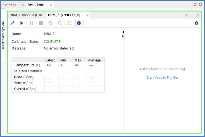
Chapter 2: Overview

Unsupported Features
       The following features are not supported in the AXI3 interface or the HBM IP:

       • Fixed addressing mode
       • QoS signaling
       • HBM GEN1 Legacy operating mode

Licensing and Ordering
       This Xilinx® LogiCORE™ IP module is provided at no additional cost with the Xilinx Vivado®
       Design Suite under the terms of the Xilinx End User License.

       Note: To verify that you need a license, check the License column of the IP Catalog. Included means that a
       license is included with the Vivado® Design Suite; Purchase means that you have to purchase a license to
       use the core.

       For more information about this core, visit the HBM enabled Virtex® UltraScale+™ device
       product page.

       Information about other Xilinx® LogiCORE™ IP modules is available at the Xilinx Intellectual
       Property page. For information about pricing and availability of other Xilinx LogiCORE IP modules
       and tools, contact your local Xilinx sales representative.

PG276 (v1.0) January 21, 2021                                                                    www.xilinx.com
                                                                            Send Feedback
AXI HBM Controller                                                                                            8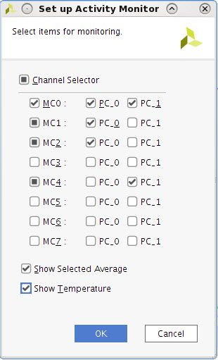
Chapter 3: Product Specification

                                                                                        Chapter 3

Product Specification
       The AXI High Bandwidth Memory Controller provides user logic access to the attached HBM
       through the AXI3 ports distributed throughout the general interconnect. Each of the 16 AXI3
       ports per stack has a throughput capacity equal to 1/16 of the total HBM bandwidth.

       Each of these ports has pipeline registers to facilitate timing closure and routing of user logic.
       Each port can optionally address the entire HBM space (global addressing) to greatly reduce the
       need for any cross channel routing in general interconnect. Alternatively, non-global addressing
       (direct addressing) limits an AXI3 port to the associated pseudo channel with the least latency.

       The eight memory controllers in a stack each have flexibility to optimize latency and utilization
       trade-offs for a given application by using different reordering or operating modes. Also, activity
       monitoring registers are provided to facilitate analysis.

       Reliability is enhanced with full datapath parity checking and optional SECDED ECC protection in
       memory. Error logging is provided by ECC status registers.

Standards
       The AXI HBM controller supports AXI3. For more information of features not included, see the
       Unsupported Features.

       Documented registers are addressable through the AMBA APB bus protocol.

PG276 (v1.0) January 21, 2021                                                              www.xilinx.com
                                                                       Send Feedback
AXI HBM Controller                                                                                      9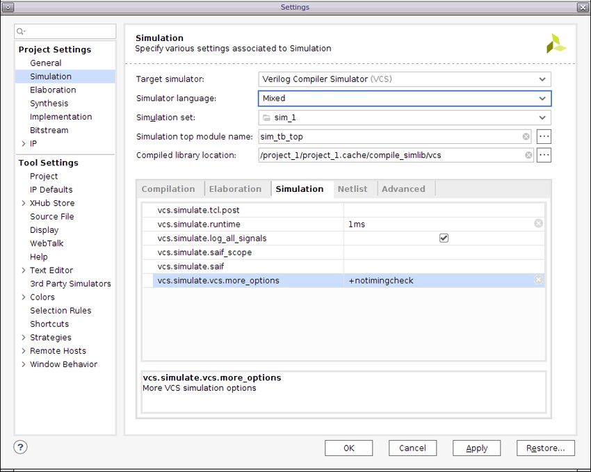
Chapter 3: Product Specification

Performance
       Maximum Frequencies

       The following table shows the maximum frequencies for the AXI HBM controller.

       Table 1: Maximum Frequencies

                           Clock                          Maximum Frequency1 (MHz)                              Notes
        AXI3 Port Clocks[15:0]                                           450                      Per AXI3 port
        AMBA APB Register Bus Clock                                      100
        Memory CLK[7:0]                                                  900                      Per HBM channel
        Notes:
        1.    Maximum frequency supported for fastest speed grade.

       Latency

       The following table shows the latency for the AXI HBM controller.

       Table 2: Latency

                                             Open Page – No
             Latency Component                                          Closed Page – Activate
                                                Activate                                                          Notes
                 Description
                                             Memory Clocks                  Memory Clocks
        AXI Port Latency – Global                    90                             108               Direct routing from AXI3 port
        addressing disabled                                                                           to aligned Memory Channel1.
        AXI Port Latency – Global              110 (Minimum)                   128 (Minimum)          Latency is dependent on the
        addressing enabled                                                                            source and destination
                                                                                                      traffic for all the ports. Thus,
                                                                                                      a maximum latency cannot
                                                                                                      be provided.
        Notes:
        1.    For more information, see Table 6: AXI Port Assignments in the Port Descriptions section.

PG276 (v1.0) January 21, 2021                                                                                     www.xilinx.com
                                                                                          Send Feedback
AXI HBM Controller                                                                                                             10
Chapter 3: Product Specification
Lateral AXI Switch Access Throughput Loss
Two lateral connections are provided between sets of 4 masters x 4 slaves within the switch,
with one lateral connected to M0 and M1, and the other connected to M2 and M3. The shared
connections limit the maximum throughput laterally to 50% of the full bandwidth, but enables
global addressing from any AXI port to any portion of the HBM. For Write cycles there is a single
dead cycle when switching between masters on the lateral channel. The throughput loss due to
this inserted cycle depends on the block size of the writes and the extent to which throughput is
switch limited, rather than HBM MC limited.
Figure 2: HBM AXI Switch Connections
M0 M1 M2 M3
M4 S6
M5 S7 M1 routing is identical to M0
M3 routing is identical to M2
S4 M6 M6/7 routing is identical to M4/5
S5 M7
S0 S1 S2 S3
For East/West transactions within an AXI Switch instance there is no lateral performance loss.
For East/West transactions which leave an AXI Switch instance there will be a lateral throughput
performance loss.
A transaction that is stalled by the AXI Master while crossing switches will continue to reserve
the lateral path, preventing its use from other channels. For example, an AXI port, reading from a
memory location that requires crossing switches, is unable to receive a full data burst and de-
asserts RREADY mid-transaction. This would cause the lateral path to remain claimed by this
transaction and unable to process transactions from other AXI channels that require the same
path.
Table 3: MC Performance Impact Per Switch Instance
MC Transaction Performance Impact
M0/1 going east to S2/S3 No
M0/1 going west to S4 or east to S7 Yes
M2/3 going west to S0/S1 No
M2/3 going east to S6 or west to S5 Yes
PG276 (v1.0) January 21, 2021 www.xilinx.com
Send Feedback
AXI HBM Controller 11Chapter 3: Product Specification
Figure 3: Switch Lateral Connections
M0 M1 M2 M3 M4 M5 M6 M7
S6
S7
M6
M7
S0 S1 S2 S3 S4 S5 S6 S7
X22063-072320
A Write sequence with near 100% MC throughput results in the largest drop in throughput due
to the extra switching cycle. As a result, smaller blocks have a larger percentage loss than larger
blocks. The following figure demonstrates the lateral throughput loss with 32-byte and 256-byte
transactions. For the 32-byte transactions two masters are each issuing three 32-byte bursts
which must laterally traverse the AXI switch. For the 256-byte transactions each master is
issuing two 256-byte bursts which must laterally traverse the AXI switch. In the 32-byte case
there is one clock inserted between each data burst for each master which results in a total of 12
clock cycles to move 6 beats of data. In the 256-byte case there is one idle clock inserted
between each 256-byte burst which results in a total of 36 clock cycles to move 32 beats of
data. Because M2 and M3 only have access to one lateral slave port, the total bandwidth for
these ports is split between the two masters. This results in a total efficiency for the 32-byte
transactions of about 25% due to the additional clock cycles for switching between masters as
well as both masters sharing a single slave port. For the 256-byte transactions these same
behaviors result in approximately 44.4% efficiency.
PG276 (v1.0) January 21, 2021 www.xilinx.com
Send Feedback
AXI HBM Controller 12Chapter 3: Product Specification
Figure 4: Switch Throughput Pattern
M2 M3
S6
S4 S5
HBM HBM
0 1 2 0 1 2
0 X 0 X 1 X 1 X 2 X 2 X
0 1 2 0 1 2
0 1 0 1
0 X 0 X 1 X 1 X
0 1 0 1
X22062-072420
Table 4: Measured Lateral Throughput Efficiency Based on 100% Page Hit Rate Write
Streams for 4H Stack
Block Size Switch Limited BW Pct
32 B 24.9%
64 B 33.3%
128 B 39.9%
256 B 44.4%
512 B 47%
PG276 (v1.0) January 21, 2021 www.xilinx.com
Send Feedback
AXI HBM Controller 13Chapter 3: Product Specification
Resource Use
Minimal CLB and block RAM resources are required to support the HBM stack controller.
Primarily the logic is used for register initialization based on the values set in the Vivado® HBM
wizard. Additional CLB resources are used for the clocks required for the design, the enabled AXI
interface(s), and the APB register interface. The following figure shows the HBM controller
initialization logic.
Figure 5: CLB-Based Initialization Logic
Block RAM
containing Configuration
config State Machine
data
APB
Temperature APB Interface HBM
Polling Bus Unisim
APB User
Interface Arbiter Primitive
XSDB Debug
Interface
X22092-073120
PG276 (v1.0) January 21, 2021 www.xilinx.com
Send Feedback
AXI HBM Controller 14Chapter 3: Product Specification
Port Descriptions
The following table shows the AXI HBM controller signals.
Table 5: AXI HBM Controller Signals1
Port Name I/O Description
AXI_xx_ACLK I Clock for the AXI Interface
AXI_xx_ARESET_N I Active-Low AXI Reset. This reset port should only be used prior to the start of data
traffic. Using it after traffic has begun will cause the AXI interface and the memory
controller to become out-of-sync.
When the switch is enabled, the IP will internally connect all of the
AXI_xx_ARESET_N pins together because the memory behaves as a single unit.
AXI_xx_ARADDR I [32:0] Read Address for 4H Stack, [33:0] Read Address for 8H Stack2
AXI_xx_ARBURST I [1:0] Address Read Burst. The fixed address burst type (2'b00) is not supported
AXI_xx_ARID I [5:0] Read Address ID Tag
AXI_xx_ARLEN I [3:0] Read Burst Length
AXI_xx_ARSIZE I [2:0] Read Burst Size
Only 256-bit size supported (3'b101)
AXI_xx_ARVALID I Read Address Valid
AXI_xx_ARREADY O Read address Ready
AXI_xx_AWADDR I [32:0] Write Address for 4H Stack, [33:0] Write Address for 8H Stack 2
AXI_xx_AWBURST I [1:0] Write Burst Type. The fixed address burst type (2'b00) is not supported.
AXI_xx_AWID I [5:0] Write Address ID
AXI_xx_AWLEN I [3:0] Write Burst Length
AXI_xx_AWSIZE I [2:0] Write Burst
Only 256-bit size supported (3'b101)
AXI_xx_AWVALID I Write Address Valid
AXI_xx_RREADY I Read Ready
AXI_xx_BREADY I Response Ready
AXI_xx_WDATA I [255:0] Write Data
AXI_xx_WLAST I Write Last
AXI_xx_WSTRB I [31:0] Write Strobe
AXI_xx_WDATA_PARITY I [31:0] Write Data
Can be used for user parity or data width expansion. User parity is calculated on a
per byte basis and the calculation is Odd. For Odd parity a 1 is asserted per byte if
the sum of the bits in that byte is Odd.
AXI_xx_WVALID I Write Valid
AXI_xx_AWREADY O Write Address Ready
AXI_xx_RDATA_PARITY O [31:0] Read Data Parity
Can be used for user parity or data width expansion. User parity is calculated on a
per byte basis and the calculation is Odd. For Odd parity a 1 is asserted per byte if
the sum of the bits in that byte is Odd.
AXI_xx_RDATA O [255:0] Read Data
AXI_xx_RID O [5:0] Read ID Tag
PG276 (v1.0) January 21, 2021 www.xilinx.com
Send Feedback
AXI HBM Controller 15Chapter 3: Product Specification
Table 5: AXI HBM Controller Signals1 (cont'd)
Port Name I/O Description
AXI_xx_RLAST O Read Last
AXI_xx_RRESP O [1:0] Read Response
AXI_xx_RVALID O Read Valid
AXI_xx_WREADY O Write Ready
AXI_xx_BID O [5:0] Response ID Tag
AXI_xx_BRESP O [1:0] Write Response
AXI_xx_BVALID O Write Response Valid
APB_y_PCLK I APB Port Clock
APB_y_PENABLE I APB Enable
APB_y_PRESET_N I APB active-Low Reset. When this bit is asserted, it resets the entire memory
interface including the controller, PHY, and memory stacks. Runs in the APB_PCLK
domain and can be asserted/deasserted asynchronously with a minimum pulse
width of one APB clock cycle.
APB_y_PSEL I APB Select
APB_y_PWRITE I APB Bus Direction
APB_y_PRDATA O [31:0] APB Read Data
APB_y_PREADY O APB Ready
APB_y_PSLVERR O APB Transfer Error
DRAM_y_STAT_CATTRIP O HBM Catastrophic Temperature Flag. This bit is asserted when a DRAM's
temperature has exceeded 120C. When this bit is asserted, ensure to immediately
disable the memory access.
DRAM_y_STAT_TEMP O [6:0] Temperature in Celsius. This is the worst-case scenario for the two memory
stacks. When the temperature of the two memory stacks is over 5°C, the highest
temperature of the two is driven out on both the DRAM_y_STAT_TEMP ports.
When the temperature of the two memory stacks is below 5°C, the lowest
temperature of the two stacks is driven out on both the DRAM_y_STAT_TEMP
ports. The update frequency is configurable. When there are two ports in the IP
for a two Stack enabled design, the data on both ports is identical because it is
driven by a single source.3
apb_complete_0 O Indicates initial configuration sequence for Stack-0 is complete
apb_complete_1 O Indicates initial configuration sequence for Stack-1 is complete
Notes:
1. There are two AXI ports per memory controller enabled and one APB port per memory stack enabled.
2. In AXI_xx_ARADDR and AXI_xx_AWADDR signals:
a. 4H Stack Bit [32], 8H Stack[33] is used to select the HBM Stack.
b. 4H Stack Bits [31:28], 8H Stack[32:29] are used to select the AXI Port.
c. 4H Stack Bits [27:5], 8H Stack[28:5] are used to access the actual HBM.
d. Bits [4:0] are unused because the AXI_xx_ARSIZE and AXI__xx_AWSIZE signals are always 3'b101 (32-byte
aligned).
3. This behavior change is implemented in the Vivado® Design Suite from 2018.3 release. Prior to 2018.3, lower 3-bits
represented the refresh rate required for the memory based on the stack temperature.
PG276 (v1.0) January 21, 2021 www.xilinx.com
Send Feedback
AXI HBM Controller 16Chapter 3: Product Specification
The following table shows the AXI port assignments in the general interconnect. This includes
the start address associated with each HBM channel, memory controller, and pseudo channel to
which it is aligned. In non-global address mode, an AXI port can only access its associated pseudo
channel. Each AXI port has a fixed address map of 2 Gb (4H Stack) or 4 Gb (8H Stack). Therefore
in non-global address mode each AXI port must be mapped to the address space with its start
address mentioned in the first column and ending before the start address of the next pseudo
channel. In global address mode each port can access all pseudo channels but with varying
performance and latency.
Table 6: AXI Port Assignments
Start Address Start Address
HBM Stack AXI Port HBM Channel/PC HBM Controller
(16 GB) (8 GB)
0x0_0000_0000 0x0_0000_0000 Left 0 A/PC0 MC0
0x0_2000_0000 0x0_1000_0000 Left 1 A/PC1 MC0
0x0_4000_0000 0x0_2000_0000 Left 2 E/PC0 MC1
0x0_6000_0000 0x0_3000_0000 Left 3 E/PC1 MC1
0x0_8000_0000 0x0_4000_0000 Left 4 B/PC0 MC2
0x0_A000_0000 0x0_5000_0000 Left 5 B/PC1 MC2
0x0_C000_0000 0x0_6000_0000 Left 6 F/PC0 MC3
0x0_E000_0000 0x0_7000_0000 Left 7 F/PC1 MC3
0x1_0000_0000 0x0_8000_0000 Left 8 C/PC0 MC4
0x1_2000_0000 0x0_9000_0000 Left 9 C/PC1 MC4
0x1_4000_0000 0x0_A000_0000 Left 10 G/PC0 MC5
0x1_6000_0000 0x0_B000_0000 Left 11 G/PC1 MC5
0x1_8000_0000 0x0_C000_0000 Left 12 D/PC0 MC6
0x1_A000_0000 0x0_D000_0000 Left 13 D/PC1 MC6
0x1_C000_0000 0x0_E000_0000 Left 14 H/PC0 MC7
0x1_E000_0000 0x0_F000_0000 Left 15 H/PC1 MC7
0x2_0000_0000 0x1_0000_0000 Right 16 A/PC0 MC8
0x2_2000_0000 0x1_1000_0000 Right 17 A/PC1 MC8
0x2_4000_0000 0x1_2000_0000 Right 18 E/PC0 MC9
0x2_6000_0000 0x1_3000_0000 Right 19 E/PC1 MC9
0x2_8000_0000 0x1_4000_0000 Right 20 B/PC0 MC10
0x2_A000_0000 0x1_5000_0000 Right 21 B/PC1 MC10
0x2_C000_0000 0x1_6000_0000 Right 22 F/PC0 MC11
0x2_E000_0000 0x1_7000_0000 Right 23 F/PC1 MC11
0x3_0000_0000 0x1_8000_0000 Right 24 C/PC0 MC12
0x3_2000_0000 0x1_9000_0000 Right 25 C/PC1 MC12
0x3_4000_0000 0x1_A000_0000 Right 26 G/PC0 MC13
0x3_6000_0000 0x1_B000_0000 Right 27 G/PC1 MC13
0x3_8000_0000 0x1_C000_0000 Right 28 D/PC0 MC14
0x3_A000_0000 0x1_D000_0000 Right 29 D/PC1 MC14
PG276 (v1.0) January 21, 2021 www.xilinx.com
Send Feedback
AXI HBM Controller 17Chapter 3: Product Specification
Table 6: AXI Port Assignments (cont'd)
Start Address Start Address
HBM Stack AXI Port HBM Channel/PC HBM Controller
(16 GB) (8 GB)
0x3_C000_0000 0x1_E000_0000 Right 30 H/PC0 MC15
0x3_E000_0000 0x1_F000_0000 Right 31 H/PC1 MC15
Note: The AXI Start addresses mentioned in the table are hard coded regardless of how many stacks are
enabled.
AXI Port Details
For signal definitions and protocol, see the AMBA AXI Protocol Specification. When user parity is
enabled, drive the correct parity value on WDATA_PARITY for Write transactions. The
RDATA_PARITY bus provides the Read data parity along with the Read data. The parity
calculation is done on a per-byte basis where a 1 is asserted if the sum of the bits in a byte is
Odd.
Each AXI port can accept 64 read transactions and 32 write transactions.
Non-AXI Ports
A single 32-bit APB register bus with 22 bits of addressing provides access to all the documented
status registers for each HBM controller stack. For naming and protocol definitions, see the
AMBA AXI Protocol Specification.
Note: apb_slv_error is not used.
There is one port per stack to indicate the end of initial configuration sequence through the
internal APB master. This port is apb_complete_0 for Stack-0 APB interface and
apb_complete_1 for Stack-1 APB interface. You need to monitor these ports and wait until
they sample high before starting any transaction on the AXI3 interface.
PG276 (v1.0) January 21, 2021 www.xilinx.com
Send Feedback
AXI HBM Controller 18Chapter 3: Product Specification
Data Path Error Protection
Figure 6: Data Path Error Protection Scheme
HBM Pseudo Channel
Host RD ECC 1b error correct data
Application (no error reported)
ECC
ECC GEN/CHK
Data Data Data Data
AXI INFC
Data 64
HOST
256 256 MC Datapath 256 256
MEM
HBM
PHY
Host
Host Host ECC or ECC or DERR
ECC WR DM (wr parity error)
WR DM
Par
GEN/CHK
GEN/CHK
CHK
Host
Datapath Datapath HBM HBM
Parity or Data Parity
Parity Parity Parity 8 Parity 2
ECC 32
WR PERR force 2bit data error
Host WR
PERR BRESP error
AXI BRESP RD PERR RDDATA error resp
RD ECC(uncorrected) RDDATA
error resp
AXI RRESP
WR PERR DERR output
DERR pin
X22061-112918
• BRESP error: Occurs if host parity is enabled and a parity error is detected in the AXI port for
any of the associated AXI Write data. An error drives 2'b10 on the BRESP port.
• RRESP error: Occurs if the corresponding read data has either a parity error or an
uncorrectable ECC error. The parity error check covers the path from HBM memory to AXI
RDATA output port. An error drives 2'b10 on the RRESP port.
Note: If parity retry is enabled, the error response will be asserted only if there is no read data transfer
without parity errors.
• DERR signal pulse: Occurs if the HBM detects a parity error on Write data received. The
DERR signal does not indicate exactly which AXI Write data command has caused the parity
error.
• WDATA error insertion: Occurs if a Write data parity error is detected within the memory
controller pipeline. Write data is corrupted to ensure that an ECC error will be detected at a
later point when the data is read.
PG276 (v1.0) January 21, 2021 www.xilinx.com
Send Feedback
AXI HBM Controller 19Chapter 4: Designing with the Core
Chapter 4
Designing with the Core
This section includes guidelines and additional information to facilitate designing with the core.
Clocking
There are three clock types that must be provided to the HBM core:
• The HBM_REF_CLK_x drives a PLL which then generates a clock for the eight memory
controllers, as well as the memory clock for the HBM stack. There is one PLL per HBM stack.
This clock must be sourced from a MMCM/BUFG, or from a BUFG. The HBM_REF_CLK_x can
be sourced from the cascading clocking sources derived from another clock. The source clock
for this derived clock must come from a GCIO pin within the same SLR as the HBM. The clock
generator driving the GCIO should have jitter less than 3 pS RMS.
• The APB_x_PCLK is used for the APB register port access. This can be asynchronous to the
other clocks. There is one APB clock port per HBM stack. The APB_x_PCLK can be sourced
from the cascading clocking source or MMCM or GCIO pin.
• The AXI_xx_ACLK is the clock for each of the AXI ports. These can be asynchronous to the
other clocks. The AXI_xx_ACLK can be sourced from the cascading clocking source or MMCM
or GCIO pins.
The global routing switch does not have a separate clock input, but rather shares one of the
AXI_xx_ACLKs. This is automatically selected by the software to be one of the clocks in the
middle of the user-selected memory controllers. This can be checked by looking at the hbm_0.v
file. There are parameters, CLK_SEL_xx, and only one has the attribute TRUE.
For maximum efficiency, it is important that the AXI clock selected is the highest frequency of all
of the AXI port clocks.
PG276 (v1.0) January 21, 2021 www.xilinx.com
Send Feedback
AXI HBM Controller 20Chapter 4: Designing with the Core
HBM Performance Concepts
The total performance of the HBM solution is dependent upon multiple factors:
• The HBM stack operating frequency
• The frequency of the AXI ports in the user application
• The HBM address map selection
• The global addressing mode
• The reordering options selected within the HBM IP
• The HBM stack temperature
The most important factor is how the user application logic is accessing the HBM through the
AXI ports. System architects must consider how all these factors interact when evaluating the
performance of the HBM memory solution in their design.
HBM Topology
The Xilinx HBM solutions are available in either 4 GB or 8 GB per stack options, with nearly all
configurations containing two stacks per FPGA. This means there is a total of 8 GB or 16 GB of
available memory for these dual stack devices.
The total data-bit width of an HBM stack is 1024 bits divided across eight channels of 128 bits
each. Each channel is serviced by a single memory controller which accesses the HBM in pseudo
channel mode, meaning two semi-independent 64-bit data channels with a shared command/
address/control (CAC) bus. A 4 GB per stack device has 4 Gb per channel, and each channel has
two 2 Gb or 256 MB pseudo channels. An 8 GB per stack device has 8 Gb per channel, and each
channel has two 4 Gb or 512 MB pseudo channels.
Most of the HBM protocol requirements and timing can be evaluated on a pseudo channel basis,
meaning that two Activate commands can be issued back to back to PC0 and PC1 without
considering tRRD. If two Activate commands are issued to the same pseudo channel back to
back, tRRD must first expire before the second Activate command can be issued.
The HBM always operates with a burst length of 4 in pseudo channel mode. The HBM protocol
closely matches that of DDR4 memory, so many of the same performance and protocol concepts
apply. The clock rate of the HBM is set in the IP configuration options in the Vivado IDE. HBM is
a double data rate (DDR) memory, so the data bus toggles at twice the interface clock rate.
PG276 (v1.0) January 21, 2021 www.xilinx.com
Send Feedback
AXI HBM Controller 21Chapter 4: Designing with the Core
Raw Throughput Evaluation
It is important to understand the raw throughput of the HBM stacks and how the user logic must
be designed to match this data rate. Each HBM stack has eight channels, each channel has a
dedicated memory controller, each memory controller is operating in pseudo channel mode, each
pseudo channel is 64 bits wide, and the data bits toggle at twice the HBM clock rate set in the IP
configuration. If the HBM IP is configured with a 900 MHz clock rate, the toggle rate for a single
HBM stack can be evaluated using the following formula:
(64 bits per pseudo channel) x (2 pseudo channels per memory controller) x (8 channels) x 900 MHz x 2
This results in 1,843,200 Mb per second per stack, or 230,400 MB per second per stack. Double
this value to 460,800 MB per second for a dual stack device.
From the user logic perspective each AXI port for the HBM is 256 bits wide and there is one AXI
port per pseudo channel in the stack. From the example above, the user logic must clock the AXI
ports at 450 MHz to match the toggle rate of the HBM when it is running at 900 MHz. This is
evaluated by the following formula:
(256 bits per AXI port) x (2 ports per memory controller) x (8 channels) x 450 MHz
This results in 1,843,200 Mb per second per stack, or 230,400 MB per second per stack. Double
this value for 460,800 MB per second for a dual stack device with 32 AXI ports.
These are the raw HBM throughput calculations but as with all traditional volatile memories the
arrays in the HBM stacks need to be refreshed to maintain data integrity. The base refresh
interval (tREFI) for the HBM stacks is 3.9 μs. For 4H devices, the refresh command period (tRFC)
is 260 ns and for 8H devices it is 350 ns. Adding in the refresh overhead to the raw throughput
of a 4H device causes the loss of approximately 7% of peak efficiency, and 8H devices lose
approximately 9%. As is the case with traditional volatile memory, tREFI decreases as the
temperature increases, so more available HBM interface time is lost to refresh overhead as the
stacks heat up. The base rate of 3.9 μs is used for temperatures from 0°C to 85°C. Between
85°C and 95°C tREFI is reduced to 1.95 μs.
AXI Considerations
The HBM IP requires a fixed AxSIZE of 0x5 for 32 bytes (256 bits) and it is recommended to have
a minimum AxLEN of 0x1 to gain higher performance for linear accesses. Undersized AXI writes
are supported by using the WSTRB port but these accesses decrease the total system
performance. This is because the same amount of HBM protocol execution and interface time is
used to service a full 32-byte Write as is used for an 8-byte Write. With this example the
effective peak bandwidth is only 25% of the theoretical maximum.
PG276 (v1.0) January 21, 2021 www.xilinx.com
Send Feedback
AXI HBM Controller 22Chapter 4: Designing with the Core
Another AXI consideration is to make sure that the AXI Write and Read addresses are aligned to
the HBM physical address space and transaction size. The lower five bits of the AWADDAR and
ARADDR should be unused to ensure that accesses align to the 32-byte HBM burst boundary.
This is because each individual Write or Read transaction on the HBM interface is a burst length
of 4 with a DQ bus width of 64 bits, resulting in a total of 32 bytes. The AXI address space is a
byte address, so 32 bytes result in 5 bits of addressing, and these are placed at the bottom of the
address space. If an AXI transaction has a non-zero value in these lower address bits, the HBM
controller must execute multiple commands on the HBM interface. In the case of an unaligned
Read operation, two Reads are required on the HBM interface to gather the data. The controller
then coalesces this to the expected payload which is delivered to the AXI Read channel. Here,
the effective bandwidth is 50% or less depending on the additional protocol churn on the HBM
interface. The same situation can occur with an unaligned Write, where a single Write request
executes as two writes on the HBM interface while using the data mask pins to mask the unused
portion of the Write payload. If ECC is enabled, an unaligned Write executes as two Read/
Modify/Write (RMW) operations. When ECC is enabled the HBM controller cannot use the Data
Mask pins so the first portion of the unaligned Write needs to be Read from the memory, then
modified by the controller for a new data payload, and finally written back to the HBM. This
process is executed twice because it requires two RMW operations to service the unaligned
Write along the HBM burst boundaries.
The last AXI consideration is that the Write and Read channels operate independently while
there is only a single electrical interface on the HBM stacks. This means that the HBM controller
only executes Write operations and then must wait for the appropriate period of protocol time to
service a bus turnaround before it can issue Read operations. For the highest possible efficiency,
the user logic should minimize bus turnarounds, maximize the amount of time spent moving data
in one direction before having to go the other way, or at least have a highly deterministic access
pattern that minimizes protocol churn for simultaneous Write and Read streams.
HBM Address Map and Protocol Considerations
To design the most efficient system architecture and user logic to access the HBM, it is important
to understand the physical address space of the HBM as well as the address map option set in
the IP configuration in the Vivado IDE. Understanding of these two aspects is required to
evaluate the HBM protocol execution. This is the largest factor in evaluating a system
performance based on the user logic AXI access pattern. The following table defines the HBM
physical address map for 4H and 8H devices.
PG276 (v1.0) January 21, 2021 www.xilinx.com
Send Feedback
AXI HBM Controller 23Chapter 4: Designing with the Core
Table 7: Physical Address Map for 4H and 8H Devices
HBM Arrangement 4H Device (4 GB per Stack) 8H Device (8 GB per Stack)
Density per Channel 4 Gb 8 Gb
Density per Pseudo Channel 2 Gb 4 Gb
Row Address RA[13:0] RA[13:0]
Column Address CA[5:1] CA[5:1]
Bank Group Address BA[3:0] SID, BA[3:0]
Bank Arrangement 16 Banks 32 Banks
4 Bank Groups with 4 Banks 8 Bank Groups with 4 Banks
Total User Address Bits 23 24
The total address space of a 4H device is 32 bits and for an 8H device it is 33 bits. The following
table describes the AXI addressing for these devices.
Table 8: AXI Addressing for 4H and 8H Devices
HBM Arrangement 4H Device (4 GB per Stack) 8H Device (8 GB per Stack)
Total Address Bits 33 total as 32:0 34 total as 33:0
Stack Select: 0 = Left 1 = Right 32 33
Destination AXI Port: 0 – 15 31:28 32:29
HBM Address Bits 27:5 28:5
Unused Address Bits 4:0 4:0
HBM operation closely follows that of traditional volatile memories and is specifically similar to
DDR4. The basics of protocol operation dictate the resulting efficiency when accessing the
memory array, and this must be a significant consideration along with the user AXI access pattern
and how the user logic is driving the AXI channels during operation.
Like DDR4, HBM uses the concept of Banks and Bank Groups for the memory and leveraging
these concepts is how to achieve a highly efficient array access pattern. 4H devices have a total
of 16 Banks, arranged as 4 Bank Groups each with 4 Banks. 8H devices have 32 Banks, arranged
as 8 Bank Groups with 4 Banks.
The HBM supports one active Row address per Bank. Protocol access times between Banks in
different Bank Groups are lower than when accessing Banks within the same Bank Group, and
the currently active Row within a Bank must be Precharged before a different Row within that
Bank can be activated. When a Row is activated within a Bank, it is recommended to perform
multiple Column accesses within that Row before changing the Row. Doing this is considered to
result in a high page hit rate, which means higher efficiency.
PG276 (v1.0) January 21, 2021 www.xilinx.com
Send Feedback
AXI HBM Controller 24Chapter 4: Designing with the Core
By default the HBM IP is set to a Row Bank Column addressing map with the Bank Group
Interleave option enabled. With these default settings, the highest order address bits are the Row
address (RAx) bits, of which only one Row address per Bank can be active at a time. The middle
address bits are the Bank address bits, which are displayed as BGx for Bank Groups and BAx for
Bank addresses. The next lowest address range is the Column address bits which are displayed as
CAx, and these are accessed by Write and Read commands.
The Bank Group Interleave option means that BG0, the least significant bit of the Bank Group
addressing, is placed as the least significant user address bit of the HBM memory map (addr[5]).
With the default address map, an AXI transaction with an AxLEN of 0x1 and AxADDR of 0x0
executes two discrete commands on the HBM interface. The first goes to Row 0, Bank Group 0,
Bank address 0, Column 0. The second goes to Row 0, Bank Group 1, Bank address 0, and
Column 0.
Having the Bank Group Interleave option with BG0 as the least significant bit is in service of
sequential memory accesses. It decreases the amount of time spent waiting for protocol
execution because the controller splits the accesses between two Banks in two separate Bank
Groups. An AXI transaction with an AxLEN of 0x1 demonstrates this behavior, but fully
leveraging these concepts for higher efficiency requires more consideration with longer
transaction lengths or leveraging traffic streams mapped to Bank addresses across Bank Groups.
The default address map option is ideal for short mixed traffic because the Bank Group Interleave
option alleviates some protocol exposure when the AxLEN is 0x1 or larger. This default address
map option also supports the AXI reordering core which can help efficiency but might increase
latency.
IMPORTANT! For 8H HBM devices the additional Bank bit is mapped to the SID bit, which is placed at
the most significant address bit within the default Row Bank Column address map.
For 8H HBM devices the additional Bank bit is mapped to the SID bit which is placed at the most
significant address bit with the default Row Bank Column address map. This is due to a limitation
with the AXI Reordering core. Take notice with the default Row Bank Column address map and
8H devices to manage their traffic master addressing to use the SID bit as the most significant
Bank Group bit. When a custom address map is used the SID bit can be placed as desired but the
AXI Reordering Core is disabled.
When the Custom Address Map option is enabled in the HBM configuration in the Vivado IDE,
more addressing options are available but the AXI Reordering Core is disabled. The Custom
Address Map option makes it possible to manually assign address bits to other locations. The
following sections discuss the concepts behind the Row Column Bank and Bank Row Column
presets. While the presets might not be an ideal match for every application, it is still possible to
manipulate any address bit to make it better suited for the use case. When the Custom Address
Map option is enabled, the Bank Group Interleave setting goes to False, but once again it is
possible to remap the BG0 bit to the least significant bit position of the address space to achieve
the same result.
PG276 (v1.0) January 21, 2021 www.xilinx.com
Send Feedback
AXI HBM Controller 25Chapter 4: Designing with the Core
Note: When the Custom Address Map option is enabled, many of the reordering options are no longer
available. Efficiency and low latency must be achieved by having well-defined traffic masters and access
patterns for the physical address map.
The Row Column Bank address map option is ideal for long sequential access patterns. This is
because for long transaction lengths, for instance AxLEN of 0x8 or longer, the majority of the
protocol exposure is hidden by Bank Group switching. This address map is best used when the
AXI transactions are only going in one direction at a time. If the traffic must change direction,
those accesses should target the same Row/Bank combinations to guarantee a page hit for the
Column access. This means when a long sequence of Writes is being serviced, the user logic
should not issue any Read requests because this causes a bus turnaround, resulting in idle
periods on the HBM interface and lowering efficiency. If the Write and Read accesses do not
target the same Row/Bank combinations, the user logic should never try to switch directions
until the current access sequence is complete. In this scenario, if a Write stream is executing and
a Read stream is trying to access a different Row/Bank combination, the controller issues
multiple Precharge and Activate commands because the new traffic stream consists only of page
misses. This causes a significant amount of idle time on the HBM interface and lowers efficiency.
The Bank Row Column address map option is ideal for designs where the user logic has
segmented traffic streams into separate Bank Group and Bank address ranges. This means
multiple traffic streams can operate independently in their own Bank Group/address
combinations and use the remaining address space as required. In a simplified example scenario,
there are two streams where one is mapped to BA0 and BA1 across all Bank Groups while
another is mapped to BA2 and BA3 across all Bank Groups. The first stream is long and
sequential and the second stream is completely random and short. The first stream maintains
high efficiency because it has a high page hit rate. The second stream with random addressing
has low efficiency, but it never targets the same Bank/Row combination as the first stream, so
high efficiency is maintained for the first stream. Without these considerations, if a traffic stream
is long and sequential while another is random, the random stream interferes with the sequential
stream and both have low efficiency.
HBM Reordering Options
The HBM IP has many reordering and refresh options available in the Reorder, Refresh, and
Power Savings options page in the Vivado IDE. When the default Row Bank Column address map
option is used you can select from the different reordering options. However, when the Custom
Address Map option is selected, many of the reordering options are disabled, except for the
Disable Dynamic Open Page option, but the Refresh and Power Savings Options remain. This is
due to dependencies within the reordering core logic and the HBM controller. To make the best
use of the reordering options with the default address map it is necessary to understand the
functional and performance implications for each of these.
PG276 (v1.0) January 21, 2021 www.xilinx.com
Send Feedback
AXI HBM Controller 26Chapter 4: Designing with the Core
The HBM solution has two levels of command reordering. The HBM memory controller itself has
a 12-entry deep command queue where it uses look ahead logic to optimize for the current state
of the HBM memory arrays and the pending commands. This is enabled by default and functions
like any other look ahead logic within a DDR controller.
The other level of reordering is a 64-entry deep AXI command queue which is available with the
default Row Bank Column address map. This can be used by selecting the Enable Request
Reordering option in the HBM configuration options in the Vivado IDE. It interacts with the
Enable Coherency in Reordering, Reorder Queue Age Limit, and Enable Close Page Reorder
options. When enabled the AXI command queue operates similarly to the standard reordering
logic in a DDR controller. The logic targets already open Bank/Row combinations to increase the
page hit rate. Accesses to different Bank Groups are promoted over accesses to the same Bank
Group. If the controller can issue an Activate immediately, these are promoted over accesses
which require a Precharge before they can be activated. Read/Write accesses are coalesced
when possible to reduce bus turnaround.
In a case where data coherency is not guaranteed by the user traffic masters, using the Enable
Coherency in Reordering option ensures that accesses with Bank/Row locality are executed in
the order they are received. If the system has latency limitations when Request Reordering is
enabled, the Reorder Queue Age Limit option can be decreased from the default value of 128.
This value means that up to 128 new commands can be serviced before a pending command is
bumped to the top of the queue. The Enable Closed Page Reorder option turns any command in
the queue to an Auto-Precharge operation. This means that every Write or Read access causes a
new Bank activation because each command is marked as Auto-Precharge. This option is useful if
the access pattern has short bursts with highly random addressing.
When evaluating system performance through simulation or in hardware, it is important to note
the implications when the AXI reordering queue is enabled. Firstly, the traffic pattern sequence
needs to be sufficiently long for the controller to enter steady state operation. If your Write
sequence is too short, you might see overly optimistic performance because the controller is
consuming the incoming commands without any backpressure. The opposite is true for the Read
sequence. If too few commands are issued the Read performance appears to be low because
most of the time is being spent on protocol overhead rather than data transfer. When evaluating
latency with the reordering queue enabled it is important to model an access pattern which
matches the user application and is sufficiently long, especially with mixed traffic, to see if the
Reorder Queue Age Limit needs to be adjusted. A good starting point for this analysis would be a
run time which covers 10 refresh cycles, or about 40 μs.
PG276 (v1.0) January 21, 2021 www.xilinx.com
Send Feedback
AXI HBM Controller 27Chapter 4: Designing with the Core
Within the HBM memory controller you can change the look ahead behavior as well as the open
or closed page policy of the controller. By default the Look Ahead Precharge and Activate
options are enabled and this follows the same concepts seen in standard DDR controllers. When
these options are enabled the controller considers the current state of the memory array as well
as the pending 12 commands in the queue, and inserts Precharge or Activate commands
opportunistically. The Disable Dynamic Open Page option forces the controller to keep a
currently active Row/Bank open until there is a discrete command to the target Bank which
requires a Row change. This is the Precharge and Activate sequence. This might be helpful for
low bandwidth traffic streams with a high level of locality in the memory array.
System-Level Considerations
The Global Addressing option allows for flexibility on accessing the HBM array by routing an AXI
command from any ingress port which the AXI Switch then routes to the destination address.
This routing is determined by the Stack Select bit, which is the most significant bit of the AXI
address. The destination AXI port is then determined by the following four address bits. The AXI
Port Assignments table in Port Descriptions gives a visual representation of the Stack and AXI
Port mapping. As described in the Lateral AXI Switch Access Throughput Loss section, there are
latency and performance implications when AXI commands are traversing the Switch. It is
important to consider these limitations along with their user logic implementation and access
pattern to determine how much traversal your use case can support and if Global Addressing is a
viable option. If excessive traversal causes too many performance issues, it might be necessary to
rearrange the traffic masters driving into the AXI ports to be closer to their destination memory
controllers.
If a user application requires low latency the Global Addressing option should be disabled
alongside the 64-entry deep AXI reordering queue. When Global Addressing is disabled the AXI
commands are no longer routed from any ingress port to any destination. In this scenario, the AXI
commands enter the ingress port and route directly to the pseudo channel attached to this AXI
port. This bypasses the AXI Switch logic and enables the lowest latency path to the memory
controller. Disabling AXI reordering also decreases latency because commands are directly
consumed by the controller and reordered in the local 12-entry deep queue.
If AXI reordering is enabled, commands might sit in the queue for some time before they are
serviced. Additionally, if a user application requires low latency, significant analysis must be
performed on the AXI access pattern by the traffic masters and the HBM memory map. HBM
follows the same basic protocol principles of DDR4, so with a well-defined access pattern, the
HBM controller options and memory map should be reviewed to ensure the highest efficiency
operation for a given use case. Each application and workload has a different solution because
the optimal results are specific to that use case.
PG276 (v1.0) January 21, 2021 www.xilinx.com
Send Feedback
AXI HBM Controller 28Chapter 4: Designing with the Core
Depending on the application, the traffic masters might only issue a single AXI ID or multiple AXI
IDs. If the master only generates a single AXI ID, transactions with the same ID are blocked on a
channel level and execute in the order in which they are received. If multiple AXI IDs are
generated, these are reordered within the AXI Reordering core if it is enabled. If the user logic
does not manage AXI IDs or accesses to ensure coherency in these scenarios, enable the Enable
Coherency in Reordering option.
Additional care should be taken when Global Addressing is enabled. The amount of time for an
AXI access to navigate through the Switch is not deterministic because it is contending with all
the other accesses and routing occurring in real time. If coherency is required and AXI reordering
is not enabled, the user logic should manage this by waiting for the AXI response signal before
issuing a subsequent access which is dependent on the first access being complete. Within the
12-entry command queue of the memory controller, coherency is always guaranteed because, as
is the case with traditional DDR controllers, it does not break Write/Read order dependency for
efficiency.
For user applications with small transaction sizes, highly random addressing, or if the traffic
master can only generate a single AXI ID, consider using the Xilinx® Random Access Memory
Attachment IP. The RAMA IP is specifically designed to assist HBM-based designs with non-ideal
traffic masters and use cases. It is capable of resizing and reordering transactions to improve
efficiency and bandwidth as well as generating substitution AXI IDs to prevent ID blocking if a
master only generates a single AXI ID. More information on the RAMA IP can be found in the
RAMA LogiCORE IP Product Guide (PG310).
PG276 (v1.0) January 21, 2021 www.xilinx.com
Send Feedback
AXI HBM Controller 29You can also read