Video Scene Change Detection v1.1 - LogiCORE IP Product Guide Vivado Design Suite - Xilinx
←
→
Page content transcription
If your browser does not render page correctly, please read the page content below
Video Scene Change
Detection v1.1

LogiCORE IP Product Guide
Vivado Design Suite

PG322 (v1.1) February 23, 2021
Table of Contents
       Chapter 1: Introduction.............................................................................................. 4
          Features........................................................................................................................................ 4
          IP Facts..........................................................................................................................................5

       Chapter 2: Overview......................................................................................................6
          Navigating Content by Design Process.................................................................................... 6
          Core Overview..............................................................................................................................6
          Feature Summary........................................................................................................................ 7
          Applications..................................................................................................................................7
          Licensing and Ordering.............................................................................................................. 8

       Chapter 3: Product Specification........................................................................... 9
          Standards..................................................................................................................................... 9
          Performance................................................................................................................................ 9
          Resource Utilization.................................................................................................................. 10
          Port Descriptions.......................................................................................................................10
          Register Space........................................................................................................................... 15
          Accessing 64-bit DDR Memory Location.................................................................................23

       Chapter 4: Designing with the Core................................................................... 24
          General Design Guidelines.......................................................................................................24
          Clocking...................................................................................................................................... 25
          Resets..........................................................................................................................................25
          Programming Sequence...........................................................................................................25

       Chapter 5: Design Flow Steps.................................................................................27
          Customizing and Generating the Core................................................................................... 27
          Interface..................................................................................................................................... 28
          Constraining the Core/Subsystem.......................................................................................... 31
          Simulation.................................................................................................................................. 32
          Synthesis and Implementation................................................................................................32

PG322 (v1.1) February 23, 2021                                                                                                       www.xilinx.com
                                                                                                      Send Feedback
Video Scene Change Detection                                                                                                                      2
Chapter 6: Example Design..................................................................................... 33
          Synthesizable Example Design................................................................................................ 35

       Chapter 7: Test Bench.................................................................................................42

       Appendix A: Verification, Compliance, and Interoperability...............43

       Appendix B: Upgrading............................................................................................. 44

       Appendix C: Application Software Development....................................... 45
          Building the BSP........................................................................................................................ 45
          Modes of Operation.................................................................................................................. 45
          Usage.......................................................................................................................................... 46

       Appendix D: Debugging............................................................................................ 48
          Finding Help on Xilinx.com...................................................................................................... 48
          Debug Tools............................................................................................................................... 49
          Hardware Debug....................................................................................................................... 50

       Appendix E: Additional Resources and Legal Notices..............................51
          Xilinx Resources.........................................................................................................................51
          Documentation Navigator and Design Hubs.........................................................................51
          References..................................................................................................................................51
          Revision History......................................................................................................................... 52
          Please Read: Important Legal Notices................................................................................... 53

PG322 (v1.1) February 23, 2021                                                                                                      www.xilinx.com
                                                                                                      Send Feedback
Video Scene Change Detection                                                                                                                     3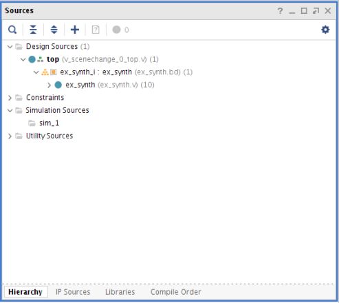
Chapter 1: Introduction

                                                                                      Chapter 1

Introduction
       The Xilinx® Video Scene Change Detection IP provides a video processing block that implements
       the scene change detection algorithm. The IP core calculates a histogram on a vertically
       subsampled luma frame for consecutive frames. The histograms of these frames are then
       compared using the sum of absolute differences (SAD). This IP core is programmable through a
       comprehensive register interface to control the frame size, video format, and subsampling value.

Features
       • Input streams can be read from memory mapped AXI4 interface or from AXI4-Stream
         interface.
       • Supports up to eight streams in the memory mapped mode and one stream in the stream
         mode.
       • Supports Y8 and Y10 formats for memory interface.
       • Supports RGB, YUV 444, YUV 422, and YUV 420 formats for stream interface.
       • Supports 8, 10, 12, and 16 bits per color component input and output on AXI4-Stream
         interface.
       • Supports one, two, or four pixel width for stream mode and one pixel width for memory
         mode.
       • Supports spatial resolutions ranging from 64 × 64 up to 8,192 × 4,320.
       • Supports 4k 60 fps in all supported device families.
       • Supports 32-bit and 64-bit DDR memory address access.

PG322 (v1.1) February 23, 2021                                                           www.xilinx.com
                                                                     Send Feedback
Video Scene Change Detection                                                                          4
Chapter 1: Introduction
IP Facts
LogiCORE™ IP Facts Table
Core Specifics
Supported Device Family1 Versal™ ACAP, UltraScale+™ Families, UltraScale™ Architecture,
Zynq®-7000 SoC, 7 series
Supported User Interfaces AXI4-Master, AXI4-Lite, AXI4-Stream2
Resources Performance and Resource Use web page
Provided with Core
Design Files Not Provided
Example Design Yes
Test Bench Not Provided
Constraints File Xilinx Design Constraints (XDC)
Simulation Model Encrypted RTL
Supported S/W Driver3 Standalone, Linux V4L2
Tested Design Flows4
Design Entry Vivado® Design Suite
Simulation For supported simulators, see the Xilinx Design Tools: Release Notes
Guide.
Synthesis Vivado® Synthesis
Support
Release Notes and Known Issues Master Answer Record: 70293
All Vivado IP Change Logs Master Vivado IP Change Logs: 72775
Xilinx Support web page
Notes:
1. For a complete list of supported devices, see the Vivado IP catalog.
2. Video protocol as defined in the "Video IP: AXI Feature Adoption" section of Vivado Design Suite: AXI Reference Guide
(UG1037).
3. Standalone driver details can be found in the Vitis directory (/Vitis//data/
embeddedsw/doc/xilinx_drivers.htm). Linux OS and driver support information is available from the Xilinx Wiki page.
4. For the supported versions of the tools, see the Xilinx Design Tools: Release Notes Guide.
5. Resource utilization is available at Performance and Resource Use web page web page.
PG322 (v1.1) February 23, 2021 www.xilinx.com
Send Feedback
Video Scene Change Detection 5Chapter 2: Overview
Chapter 2
Overview
Navigating Content by Design Process
Xilinx® documentation is organized around a set of standard design processes to help you find
relevant content for your current development task. All Versal™ ACAP design process Design
Hubs can be found on the Xilinx.com website. This document covers the following design
processes:
• Hardware, IP, and Platform Development: Creating the PL IP blocks for the hardware
platform, creating PL kernels, subsystem functional simulation, and evaluating the Vivado®
timing, resource use, and power closure. Also involves developing the hardware platform for
system integration. Topics in this document that apply to this design process include:
• Port Descriptions
• Clocking
• Resets
• Customizing and Generating the Core
• Chapter 6: Example Design
Core Overview
The Xilinx® Video Scene Change Detection core detects scene change between two consecutive
video frames received on either memory interface or stream interface. Memory or stream mode
can be selected from the IP GUI.
PG322 (v1.1) February 23, 2021 www.xilinx.com
Send Feedback
Video Scene Change Detection 6Chapter 2: Overview
Feature Summary
The Video Scene Change Detection IP is a configurable IP core that can read up to eight video
streams in the memory mode and one video stream in the stream mode. In the memory mode,
input is read from the memory mapped AXI4 interface. In the stream mode, input is read from
the AXI4-Stream interface and the output stream is same as the received input stream.
The Video Scene Change Detection IP supports resolutions ranging from 64 × 64 to 8,192 ×
4,320 with up to three color components, each of 8, 10, 12, and 16 bits. The Video Scene
Change Detection IP sends the interrupt signals after generating the SAD values for all the input
streams of every frame. In case of the memory mode, the SAD values are calculated for each
input stream one after the other sequentially and the interrupt is generated after the SAD
calculation of final stream. On interrupt generation, the SAD values are read from the SAD
registers for configured number of streams to compare them with a user decided threshold value
to determine if a scene change has occurred. In the memory mode, you can dynamically
configure the buffer addresses from where the input video stream is read.
Applications
The Video Scene Change Detection core is used for the following purposes:
• Video surveillance
• Video streaming
• Video conferencing
One of the applications of the Video Scene Change Detection IP is that it can be used with the
Zynq UltraScale+™ VCU subsystem. It helps the VCU subsystem to identify when to update the
reference frame for better performance while encoding streams. This is done using the Video
Scene Change Detection IP interrupt flag. It sends fewer frames that help in reducing the
compressed stream size, thereby saving bandwidth.
In the VCU subsystem, the encoder rate control logic works based on the previous history and
statistics gathered during the encoding session. When a scene change happens, the complexity
of the frame changes and previously calculated statistics may not hold good. The rate control
logic takes longer to adjust to the new content. If the source provides the scene change
detection flag along with the input buffer encoder, the rate control logic can quickly adjust its
statistics and prevent overshoot/undershoot in the bitrate. This results in updating the reference
frame for better performance.
PG322 (v1.1) February 23, 2021 www.xilinx.com
Send Feedback
Video Scene Change Detection 7Chapter 2: Overview
Licensing and Ordering
This Xilinx® LogiCORE™ IP module is provided at no additional cost with the Xilinx Vivado®
Design Suite under the terms of the Xilinx End User License.
Note: To verify that you need a license, check the License column of the IP Catalog. Included means that a
license is included with the Vivado® Design Suite; Purchase means that you have to purchase a license to
use the core.
For more information about this core, visit the Video Scene Change Detection product web page.
Information about other Xilinx® LogiCORE™ IP modules is available at the Xilinx Intellectual
Property page. For information about pricing and availability of other Xilinx LogiCORE IP modules
and tools, contact your local Xilinx sales representative.
PG322 (v1.1) February 23, 2021 www.xilinx.com
Send Feedback
Video Scene Change Detection 8Chapter 3: Product Specification
Chapter 3
Product Specification
Standards
The Video Scene Change Detection IP is compliant with the AXI4-Stream Video Protocol, AXI4-
Lite interconnect, and memory mapped AXI4 interface standards. For additional information, see
the Video IP: AXI Feature Adoption section of the Vivado Design Suite: AXI Reference Guide
(UG1037).
Performance
Maximum Frequencies
The following are typical clock frequencies for the target devices:
• UltraScale+™ devices with -1 speed grade or higher: 300 MHz
• Virtex®-7 and Virtex® UltraScale™ devices with -2 speed grade or higher: 300 MHz
• Kintex®-7 and Kintex® UltraScale™ devices with -2 speed grade or higher: 300 MHz
• Artix®-7 devices with -2 speed grade or higher: 150 MHz
• Versal™ ACAP devices with -1 speed grade or higher: 300 MHz
The maximum achievable clock frequency can vary. The maximum achievable clock frequency
and all resource counts can be affected by other tool options, additional logic in the device, using
a different version of Xilinx® tools, and other factors.
PG322 (v1.1) February 23, 2021 www.xilinx.com
Send Feedback
Video Scene Change Detection 9Chapter 3: Product Specification
Throughput
The Video Scene Change Detection IP supports bi-directional data throttling between its AXI4-
Stream slave and master intefaces. If the slave side data source is not providing valid data
samples (s_axis_video_tvalid is not asserted), the core cannot produce valid output
samples after its internal buffers are depleted. Similarly, if the master side interface is not ready
to accept valid data samples (m_axis_video_tready is not asserted) the core cannot accept
valid input samples after its buffers are full.
Latency
The following examples explain the latency requirements for the Video Scene Change Detection
IP in both stream and memory based modes:
• Stream mode: In the stream mode, 4K video subsampled at a subsampling factor of 16 results
in 3840*2160/16 = 518, 400 samples. If the IP processes 1 sample per clock at 100 MHz, it
takes 518K/100M = 5.2 ms to pass all samples through the IP. The IP would consume 518,
400 bytes to complete this task. In this mode, the data passes from input to output. The IP
needs to handle complete 4K data when configured to a maximum resolution of 4K. The IP
need to run at 2 samples per clock at 300 MHz. There is no bandwidth requirement in the
stream mode.
• Memory mode: In the memory mode, the IP does not need more than 4K/16 performance for
subsampling at 16. You can cover that with 1 pixel per clock. In this mode, processing 4K
video requires a peak bandwidth of 1000/5.2 * 518K = ~100 MB/s. Running the IP slower
consumes less bandwidth. The latency is still 5.2 ms to get the SAD value in the output
though you do not get any output samples.
Resource Utilization
For full details about performance and resource use, visit the Performance and Resource Use web
page.
Port Descriptions
The Video Scene Change Detection IP uses industry standard control and data interfaces to
connect to other system components. The following sections describe the various interfaces
available within the core. The following figure illustrates the Video Scene Change Detection IP
I/O diagram in memory mode. In this configuration, the IP has two AXI interfaces:
• AXI4-Lite control interface (s_axi_CTRL)
• Memory mapped AXI4 interface (m_axi_mm_video)
PG322 (v1.1) February 23, 2021 www.xilinx.com
Send Feedback
Video Scene Change Detection 10Chapter 3: Product Specification
Figure 1: Scene Change Detection IP I/O Diagram Memory Mode
The following figure illustrates the Video Scene Change Detection IP I/O diagram for stream
based mode. In this configuration, the IP has three AXI interfaces:
• AXI4-Lite control interface (s_axi_CTRL)
• AXI4-Stream streaming video input (s_axis_video)
• AXI4-Stream streaming video output (m_axis_video)
Figure 2: Scene Change Detection IP I/O Diagram Stream Mode
Common Interface Signals
The following table summarizes the signals which are either shared by or not part of the
dedicated AXI4-Stream, memory mapped AXI4 data, or AXI4-Lite control interfaces.
Table 1: Common Interface Signals
Signal Name I/O Width Description
ap_clk I 1 Video core clock
ap_rst_n I 1 Video core active-Low reset
interrupt O 1 Interrupt Request Pin
The ap_clk and ap_rst_n signals are shared between the core, memory mapped AXI4 data
interfaces, and the AXI4-Lite control interface.
PG322 (v1.1) February 23, 2021 www.xilinx.com
Send Feedback
Video Scene Change Detection 11Chapter 3: Product Specification
• ap_clk: The memory mapped AXI4 and AXI4-Lite interfaces must be synchronous to the core
clock signal ap_clk. All memory mapped AXI4 interface input signals and AXI4-Lite control
interface input signals are sampled on the rising edge of ap_clk.
• ap_rst_n: The ap_rst_n pin is an active-Low, synchronous reset input pertaining to both
AXI4-Lite and memory mapped AXI4 interfaces. When ap_rst_n is set to 0, the core resets
at the next rising edge of ap_clk.
• interrupt: The interrupt status output bus can be integrated with an external interrupt
controller that has independent interrupt enable/mask, interrupt clear, and interrupt status
registers that allow interrupt aggregation to the system processor.
AXI4-Stream Video Interface
The Video Scene Change Detection IP has AXI4-Stream video input and output interfaces named
s_axis_video and m_axis_video respectively, when the stream mode is enabled.
Both video streaming interfaces follow the interface specification as defined in the Video IP
chapter of the Vivado Design Suite: AXI Reference Guide (UG1037). The video AXI4-Stream
interface can be single, dual, or quad pixels per clock and can support 8, 10, 12, or 16 bits per
component. The streaming interface configuration (samples per clock and bits per component) is
chosen at the IP level and applies to all instances of the AXI4-Stream interface.
The following tables explain the pixel mapping of an AXI4-Stream interface with two pixels per
clock and 10 bits per component configuration for all supported video color formats:
Table 2: Dual Pixels Per Clock, 10 Bits Per Component Mapping for RGB
69:60 59:50 49:40 39:30 29:20 19:10 9:0
Zero padding R1 B1 G1 R0 B0 G0
Table 3: Dual Pixels Per Clock, 10 Bits Per Component Mapping for YUV 4:4:4
69:60 59:50 49:40 39:30 29:20 19:10 9:0
Zero padding V1 U1 Y1 V0 U0 Y0
Table 4: Dual Pixels Per Clock, 10 Bits Per Component Mapping for YUV 4:2:2
69:60 59:50 49:40 39:30 29:20 19:10 9:0
Zero padding Zero padding Zero padding V0 Y1 U0 Y0
The following table shows the interface signals for input and output AXI4-Stream video
streaming interfaces.
PG322 (v1.1) February 23, 2021 www.xilinx.com
Send Feedback
Video Scene Change Detection 12Chapter 3: Product Specification
Table 5: AXI4-Stream Interface Signals
Signal Name I/O Width Description
s_axis_tdata I floor(((3× bits_per_component× Input Data
pixels_per_clock) + 7) / 8) × 8
s_axis_tready O 1 Input Ready
s_axis_tvalid O 1 Input Valid
s_axis_tdest I 1 Input Data Routing Identifier
s_axis_tkeep I (s_axis_video_tdata width) / 8 Input byte qualifier that indicates whether the content
of the associated byte of TDATA is processed as part of
the data stream.
s_axis_tlast I 1 Input End of Line
s_axis_tstrb I (s_axis_video_tdata width) / 8 Input byte qualifier that indicates whether the content
of the associated byte of TDATA is processed as a data
byte or a position byte.
s_axis_tuser I 1 Input Start of Frame
m_axis_tdata O floor(((3 × bits_per_component× Output Data
pixels_per_clock) + 7) / 8) × 8
m_axis_tdest O 1 Output Data Routing Identifier
m_axis_tid O 1 Output Data Stream Identifier
m_axis_tkeep O (m_axis_video_tdata width) / 8 Output byte qualifier that indicates whether the content
of the associated byte of TDATA is processed as part of
the data stream.
m_axis_tlast O 1 Output End of Line
m_axis_tready I 1 Output Ready
m_axis_tstrb O (m_axis_video_tdata width) / 8 Output byte qualifier that indicates whether the content
of the associated byte of TDATA is processed as a data
byte or a position byte.
m_axis_tuser O 1 Output Start of Frame
m_axis_tvalid O 1 Output Valid
Notes:
1. All video streaming interfaces run at the IP core clock speed, ap_clk.
2. For default values required to drive the AXI4-Stream interface signals that are not present in upstream or
downstream connected IPs, see the IP Using AXI4-Stream Video Protocol section of Vivado Design Suite: AXI Reference
Guide (UG1037).
Memory Mapped AXI4 Interface
There is a memory mapped AXI4 interface named m_axi_mm_video. The memory mapped
AXI4 interface runs on the ap_clk clock domain. The signals follow the specification as defined
in the Vivado Design Suite: AXI Reference Guide (UG1037). The following table shows the pixel
formats in the memory supported by the Video Scene Change Detection IP.
PG322 (v1.1) February 23, 2021 www.xilinx.com
Send Feedback
Video Scene Change Detection 13Chapter 3: Product Specification
Table 6: Memory Mode Pixel Formats
Video
Description Bits Per Component Bytes Per Pixel
Format
Y8 Packed luma only 8 1 byte per pixel
Y10 Packed luma only 10 4 bytes per 3 pixel
The following sections explain the expected pixel mappings in memory for each of the listed
formats.
Y8 Format
Packed luma-only eight bits per component. Every luma-only pixel in the memory is represented
with 8 bits. The images need to be stored in the memory in raster order, that is, top-left pixel
first, bottom-right pixel last. Y8 is presented as YUV 4:4:4 on the AXI4-Stream interface.
Table 7: Y8 Format
7:0
Y
Y10 Format
Packed luma-only 10 bits per component. Every three luma-only pixels in the memory is
represented with 32 bits. The images need be stored in the memory in raster order, that is, top-
left pixel first, bottom-right pixel last. Y10 is presented as YUV 4:4:4 on the AXI4-Stream
interface.
Table 8: Y10 Format
9:0 19:10 29:20 31:30
Y0 Y1 Y2 X
AXI4-Lite Control Interface
The AXI4-Lite interface allows you to dynamically control the parameters within the core. The
configuration can be accomplished by using an AXI4-Lite master state machine, an embedded
Arm® processor, or a soft system processor such as MicroBlaze™ processor. The Video Scene
Change Detection IP can be controlled through the AXI4-Lite interface by using functions
provided by the driver in the Vitis™ software platform. Another method is by performing read
and write transactions to the register space, but this method is only used when the first method
is not available. The following table shows the AXI4-Lite control interface signals. This interface
runs at the ap_clk clock.
PG322 (v1.1) February 23, 2021 www.xilinx.com
Send Feedback
Video Scene Change Detection 14Chapter 3: Product Specification
Table 9: AXI4-Lite Control Interface Signals
Signal Name I/O Width Description
s_axi_ctrl_aresetn I 1 Reset
s_axi_ctrl_aclk I 1 Clock
s_axi_ctrl_awaddr I 18 Write Address
s_axi_ctrl_awprot I 3 Write Address Protection
s_axi_ctrl_awvalid I 1 Write Address Valid
s_axi_ctrl_awready O 1 Write Address Ready
s_axi_ctrl_wdata I 32 Write Data
s_axi_ctrl_wstrb I 4 Write Data Strobe
s_axi_ctrl_wvalid I 1 Write Data Valid
s_axi_ctrl_wready O 1 Write Data Ready
s_axi_ctrl_bresp O 2 Write Response
s_axi_ctrl_bvalid O 1 Write Response Valid
s_axi_ctrl_bready I 1 Write Response Ready
s_axi_ctrl_araddr I 18 Read Address
s_axi_ctrl_arprot I 3 Read Address Protection
s_axi_ctrl_arvalid I 1 Read Address Valid
s_axi_ctrl_aready O 1 Read Address Ready
s_axi_ctrl_rdata O 32 Read Data
s_axi_ctrl_rresp O 2 Read Data Response
s_axi_ctrl_rvalid O 1 Read Data Valid
s_axi_ctrl_rready I 1 Read Data Ready
Register Space
The Video Scene Change Detection IP has specific registers which allow you to control the
operation of the core. All registers have an initial value of zero. The following table provides a
detailed description of all the registers that apply globally to the IP.
PG322 (v1.1) February 23, 2021 www.xilinx.com
Send Feedback
Video Scene Change Detection 15Chapter 3: Product Specification
Table 10: Register Address Space
Address (hex)
Register Name Access Type Register Description
BASEADDR+
0x0000 Control R/W
Bit[0] = ap_start
Bit[1] = ap_done
Bit[2] = ap_idle
Bit[3] = ap_ready
Bit[5] = Flush pending AXI transactions
Bit[6] = Flush done
Bit[7] = auto_restart
Others = Reserved
0x0004 Global Interrupt Enable R/W
Bit[0] = Global interrupt enable
Others = Reserved
0x0008 IP Interrupt Enable R/W
Bit[0] = Channel 0 (ap_done)
Bit[1] = Channel 1 (ap_ready)
Others = Reserved
0x000C IP Interrupt Status R/TOW1
Register Bit[0] = Channel 0 (ap_done)
Bit[1] = Channel 1 (ap_ready)
Others = Reserved
0x00010 HwReg_width_0 R/W
Bit[15] to Bit[0] = HwReg_width_0[15:0]
(Active width of stream in pixels)
Others = Reserved
0x0018 HwReg_height_0 R/W
Bit[15] to Bit[0] = HwReg_height_0[15:0]
(Active number of lines of stream)
Others = Reserved
0x0020 HwReg_stride_0 R/W
Bit[15] to Bit[0] = HwReg_stride_0[15:0]
(Stride in bytes)
Others = Reserved
0x0028 HwReg_video_format_0 R/W
Bit[15] to Bit[0] =
HwReg_video_format_0[15:0]
Others = Reserved
0x0030 HwReg_subsample_0 R/W
Bit[15] to Bit[0] = HwReg_subsample_0[15:0]
Others = Reserved
0x0038 HwReg_sad0 R
Bit[31] to Bit[0] = HwReg_sad0[31:0]
Others = Reserved
PG322 (v1.1) February 23, 2021 www.xilinx.com
Send Feedback
Video Scene Change Detection 16Chapter 3: Product Specification
Table 10: Register Address Space (cont'd)
Address (hex)
Register Name Access Type Register Description
BASEADDR+
0x0040 HwReg_frm_buffer0_V R/W
Bit[31] to Bit[0] = HwReg_frm_buffer0_V[31:0]
Others = Reserved
0x00110 HwReg_width_1 R/W
Bit[15] to Bit[0] = HwReg_width_1[15:0]
Others = Reserved
0x00118 HwReg_height_1 R/W
Bit[15] to Bit[0] = HwReg_height_1[15:0]
Others = Reserved
0x00120 HwReg_stride_1 R/W
Bit[15] to Bit[0] = HwReg_stride_1[15:0]
Others = Reserved
0x00128 HwReg_video_format_1 R/W
Bit[15] to Bit[0] =
HwReg_video_format_1[15:0]
Others = Reserved
0x00130 HwReg_subsample_1 R/W
Bit[15] to Bit[0] = HwReg_subsample_1[15:0]
Others = Reserved
0x00138 HwReg_sad1 R
Bit[31] to Bit[0] = HwReg_sad1[31:0]
Others = Reserved
0x00140 HwReg_frm_buffer1_V R/W
Bit[31] to Bit[0] = HwReg_frm_buffer1_V[31:0]
Others = Reserved
0x00210 HwReg_width_2 R/W
Bit[15] to Bit[0] = HwReg_width_2[15:0]
Others = Reserved
0x00218 HwReg_height_2 R/W
Bit[15] to Bit[0] = HwReg_height_2[15:0]
Others = Reserved
0x00220 HwReg_stride_2 R/W
Bit[15] to Bit[0] = HwReg_stride_2[15:0]
Others = Reserved
0x00228 HwReg_video_format_2 R/W
Bit[15] to Bit[0] =
HwReg_video_format_2[15:0]
Others = Reserved
0x00230 HwReg_subsample_2 R/W
Bit[15] to Bit[0] = HwReg_subsample_2[15:0]
Others = Reserved
PG322 (v1.1) February 23, 2021 www.xilinx.com
Send Feedback
Video Scene Change Detection 17Chapter 3: Product Specification
Table 10: Register Address Space (cont'd)
Address (hex)
Register Name Access Type Register Description
BASEADDR+
0x00238 HwReg_sad2 R
Bit[31] to Bit[0] = HwReg_sad2[31:0]
Others = Reserved
0x00240 HwReg_frm_buffer2_V R/W
Bit[31] to Bit[0] = HwReg_frm_buffer2_V[31:0]
Others = Reserved
0x00310 HwReg_width_3 R/W
Bit[15] to Bit[0] = HwReg_width_3[15:0]
Others - Reserved
0x00318 HwReg_height_3 R/W
Bit[15] to Bit[0] = HwReg_height_3[15:0]
Others = Reserved
0x00320 HwReg_stride_3 R/W
Bit[15] to Bit[0] = HwReg_stride_3[15:0]
Others = Reserved
0x00328 HwReg_video_format_3 R/W
Bit[15] to Bit[0] =
HwReg_video_format_3[15:0]
Others = Reserved
0x00330 HwReg_subsample_3 R/W
Bit[15] to Bit[0] = HwReg_subsample_3[15:0]
Others = Reserved
0x00338 HwReg_sad3 R
Bit[31] to Bit[0] = HwReg_sad3[31:0]
Others = Reserved
0x00340 HwReg_frm_buffer3_V R/W
Bit[31] to Bit[0] = HwReg_frm_buffer3_V[31:0]
Others = Reserved
0x00410 HwReg_width_4 R/W
Bit[15] to Bit[0] = HwReg_width_4[15:0]
Others - Reserved
0x00418 HwReg_height_4 R/W
Bit[15] to Bit[0] = HwReg_height_4[15:0]
Others = Reserved
0x00420 HwReg_stride_4 R/W
Bit[15] to Bit[0] = HwReg_stride_4[15:0]
Others = Reserved
0x00428 HwReg_video_format_4 R/W
Bit[15] to Bit[0] =
HwReg_video_format_4[15:0]
Others = Reserved
PG322 (v1.1) February 23, 2021 www.xilinx.com
Send Feedback
Video Scene Change Detection 18Chapter 3: Product Specification
Table 10: Register Address Space (cont'd)
Address (hex)
Register Name Access Type Register Description
BASEADDR+
0x00430 HwReg_subsample_4 R/W
Bit[15] to Bit[0] = HwReg_subsample_4[15:0]
Others = Reserved
0x00438 HwReg_sad4 R
Bit[31] to Bit[0] = HwReg_sad4[31:0]
Others = Reserved
0x00440 HwReg_frm_buffer4_V R/W
Bit[31] to Bit[0] = HwReg_frm_buffer4_V[31:0]
Others = Reserved
0x00510 HwReg_width_5 R/W
Bit[15] to Bit[0] = HwReg_width_5[15:0]
Others - Reserved
0x00518 HwReg_height_5 R/W
Bit[15] to Bit[0] = HwReg_height_5[15:0]
Others = Reserved
0x00520 HwReg_stride_5 R/W
Bit[15] to Bit[0] = HwReg_stride_5[15:0]
Others = Reserved
0x00528 HwReg_video_format_5 R/W
Bit[15] to Bit[0] =
HwReg_video_format_5[15:0]
Others = Reserved
0x00530 HwReg_subsample_5 R/W
Bit[15] to Bit[0] = HwReg_subsample_5[15:0]
Others = Reserved
0x00538 HwReg_sad5 R
Bit[31] to Bit[0] = HwReg_sad5[31:0]
Others = Reserved
0x00540 HwReg_frm_buffer5_V R/W
Bit[31] to Bit[0] = HwReg_frm_buffer5_V[31:0]
Others = Reserved
0x00610 HwReg_width_6 R/W
Bit[15] to Bit[0] = HwReg_width_6[15:0]
Others - Reserved
0x00618 HwReg_height_6 R/W
Bit[15] to Bit[0] = HwReg_height_6[15:0]
Others = Reserved
0x00620 HwReg_stride_6 R/W
Bit[15] to Bit[0] = HwReg_stride_6[15:0]
Others = Reserved
PG322 (v1.1) February 23, 2021 www.xilinx.com
Send Feedback
Video Scene Change Detection 19Chapter 3: Product Specification
Table 10: Register Address Space (cont'd)
Address (hex)
Register Name Access Type Register Description
BASEADDR+
0x00628 HwReg_video_format_6 R/W
Bit[15] to Bit[0] =
HwReg_video_format_6[15:0]
Others = Reserved
0x00630 HwReg_subsample_6 R/W
Bit[15] to Bit[0] = HwReg_subsample_6[15:0]
Others = Reserved
0x00638 HwReg_sad6 R
Bit[31] to Bit[0] = HwReg_sad6[31:0]
Others = Reserved
0x00640 HwReg_frm_buffer6_V R/W
Bit[31] to Bit[0] = HwReg_frm_buffer6_V[31:0]
Others = Reserved
0x00710 HwReg_width_7 R/W
Bit[15] to Bit[0] = HwReg_width_7[15:0]
Others - Reserved
0x00718 HwReg_height_7 R/W
Bit[15] to Bit[0] = HwReg_height_7[15:0]
Others = Reserved
0x00720 HwReg_stride_7 R/W
Bit[15] to Bit[0] = HwReg_stride_7[15:0]
Others = Reserved
0x00728 HwReg_video_format_7 R/W
Bit[15] to Bit[0] =
HwReg_video_format_7[15:0]
Others = Reserved
0x00730 HwReg_subsample_7 R/W
Bit[15] to Bit[0] = HwReg_subsample_7[15:0]
Others = Reserved
0x00738 HwReg_sad7 R
Bit[31] to Bit[0] = HwReg_sad7[31:0]
Others = Reserved
0x00740 HwReg_frm_buffer7_V R/W
Bit[31] to Bit[0] = HwReg_frm_buffer7_V[31:0]
Others = Reserved
0x00780 HwReg_stream_enable R/W
Bit[15] to Bit[0] = HwReg_stream_enable[15:0]
Others = Reserved
Notes:
1. TOW = Toggle on Write
PG322 (v1.1) February 23, 2021 www.xilinx.com
Send Feedback
Video Scene Change Detection 20Chapter 3: Product Specification
Control (0x0000) Register
This register controls the operation of the video scene change detection. Bit[0] of the control
register, ap_start, kicks off the core from the software. Writing 1 to this bit, starts the core to
generate a video frame. To set the core in free running mode, Bit[7] of this register, auto_restart,
must be set to 1. Bits[3:1] are reserved for future use.
Bit[5] is for flushing pending AXI transactions. This bit should be set and held (until reset) by the
software to flush pending transactions. When this is set, the hardware is expecting a hard reset.
Bit[6] is the flush status bit and is asserted when the flush is done. Bit[5] and Bit[6] are valid only
when the IP is running in the memory mode.
Global Interrupt Enable (0x0004) Register
This register is the master control for all interrupts. Bit[0] can be used to enable/disable all core
interrupts.
IP Interrupt Enable (0x0008) Register
This register allows interrupts to be enabled selectively. Currently, two interrupt sources are
available; ap_done and ap_ready. ap_done is triggered after the frame processing is complete,
while ap_ready is triggered after the core is ready to start processing the next frame.
IP Interrupt Status (0x000C) Register
This is a dual purpose register. When an interrupt occurs, the corresponding interrupt source bit
is set in this register. In readback mode (Get status), the interrupting source can be determined. In
writeback mode (Clear interrupt), the requested interrupt source bit is cleared.
IP HwReg_Width_0 (0x0010) Register
This register allows you to program the width of the first input color image in a batch of up to
eight streams for memory based mode. This register is also applicable for the stream based mode
which supports only one stream. Supported values are between 64 and the value provided in the
Maximum Number of Columns field in the Vivado® Integrated Design Environment (IDE). To
avoid processing errors, you should restrict the values written to this register to the range
supported by the core instance.
PG322 (v1.1) February 23, 2021 www.xilinx.com
Send Feedback
Video Scene Change Detection 21Chapter 3: Product Specification
IP HwReg_Height_0 (0x0018) Register
This register allows you to program the height of the first input color image in a batch of up to
maximum 8 streams for memory based mode. This register is also applicable for the stream based
mode which supports only one stream. Supported values are between 64 and the value provided
in the Maximum Number of Rows field in the Vivado Integrated Design Environment (IDE). To
avoid processing errors, you should restrict the values written to this register to the range
supported by the core instance.
IP HwReg_stride_0 (0x0020) Register
This register allows you to program the stride required for the height of the first input color
image in a batch of up to 8 streams for memory based mode. This register is not applicable for IP
stream based mode operation.
IP HwReg_video_format_0 (0x0028) Register
This register allows to program the pixel format of the first input image which is to be read from
the source buffer. For memory based mode, use 24 for Y8 or 25 for Y10. For stream based mode,
use 0 for RGB, 1 for YUV444, 2 for YUV422, and 3 for YUV420.
IP HwReg_subsample_0 (0x0030) Register
This register allows you to program the vertical subsampling factor of the first input color image
in a batch of up to eight streams for memory based mode. This is also applicable for single stream
in the stream based mode. Instead of sampling every line to calculate the histogram, the IP uses
this register value to sample only specific lines of the frame. Valid values are 2, 4, 8, 16, 32, or 64.
Typical value to be used is 16. To avoid processing errors, you should restrict the values written
to this register to the range supported by the core instance.
IP HwReg_sad0 (0x0038) Register
This is a read only register that returns the value of the SAD between current and previous
histogram of the first input color image in a batch of up to eight streams for memory based
mode. This register is also applicable for the stream based mode.
The final scene change determination is made as shown in the following equation. While the
threshold is programmable, a good default value to start with is 0.5.
SAD > threshold
width*height
subsample factor
PG322 (v1.1) February 23, 2021 www.xilinx.com
Send Feedback
Video Scene Change Detection 22Chapter 3: Product Specification
IP HwReg_frm_buffer0_V (0x0040) Register
In the memory based mode, this register specifies the frame buffer address that holds the luma
pixel data for the first stream. The address needs to be aligned to the data size of the memory
mapped AXI4 interface. For the Video Scene Change Detection IP, the data size of the memory
mapped AXI4 interface is 32. This register is not applicable when the IP is working in the stream
mode.
If the IP is configured to a 64 bit address width in the IP GUI, the IP internally creates another
register in the register space by adding 0x4 to the existing buffer address register offset. For
example, HwReg_frm_buffer0_V register addresses are 0x0040 and 0x0044. Register
addresses for all outputs are also calculated in a similar way.
IP HwReg_stream_enable (0x00780) Register
This register need to be programmed as per the streams executed as part of a batch for memory
based mode. Bit 0 is for stream 1, bit 1 is for stream 2, likewise bit 7 is for stream 8. This register
is not applicable for stream base mode operation of the IP as there is only one stream.
IMPORTANT! The registers related to the first input stream are described above, the same description is
applicable for the remaining seven input streams for memory based mode of operation. See Register
Address Space table for the address offsets of the registers related to the remaining seven output streams.
The registers ending with _0 are also mentioned in the register address space table. These registers are also
applicable for stream mode.
Accessing 64-bit DDR Memory Location
Perform the following steps to access the 64-bit DDR memory location:
1. Change the IP address width to 64-bit in the IP GUI.
2. In the Vivado® address editor, unmap the HP0_DDR_LOW base name which has
0x0000_0000 offset address with 2G band.
3. Auto assign addresses to map DDR_LOW and DDR_HIGH address spaces for 64-bit mode.
4. Vivado Design Suit will get DDR_HIGH offset address as 0x0000_0008_0000_0000 with
32G band. The IP can use any address as source/destination buffer address.
PG322 (v1.1) February 23, 2021 www.xilinx.com
Send Feedback
Video Scene Change Detection 23Chapter 4: Designing with the Core
Chapter 4
Designing with the Core
This section includes guidelines and additional information to facilitate designing with the core.
General Design Guidelines
Use the Example Design
Each instance of the Video Scene Change Detection core created by the Vivado design tool is
delivered with an example design that can be implemented in a device and then simulated. This
design can be used as a starting point for your own design or can be used to sanity-check your
application in the event of difficulty. See the Example Design content for information about using
and customizing the example designs for the core.
Registering Signals
To simplify timing and increase system performance in a programmable device design, keep all
inputs and outputs registered between the user application and the core. This means that all
inputs and outputs from the user application should come from, or connect to, a flip-flop. While
registering signals might not be possible for all paths, it simplifies timing analysis and makes it
easier for the Xilinx® tools to place and route the design.
Recognize Timing Critical Signals
The constraints provided with the example design identify the critical signals and timing
constraints that should be applied.
Make Only Allowed Modifications
You should not modify the core. Any modifications can have adverse effects on system timing
and protocol compliance. Supported user configurations of the core can only be made by
selecting the options in the customization IP dialog box when the core is generated.
PG322 (v1.1) February 23, 2021 www.xilinx.com
Send Feedback
Video Scene Change Detection 24Chapter 4: Designing with the Core
Clocking
The Video Scene Change Detection IP has only one clock domain. All interfaces in the IP such as,
AXI4-Lite, memory mapped AXI4, and AXI4-Stream interfaces use the ap_clk pin as a clock
source.
Resets
The Video Scene Change Detection IP has ap_rst_n pin as a hardware reset option. No
software reset option is available. The external reset pulse needs to be held for 16 or more
ap_clk cycles to reset the core. The ap_rst_n signal is synchronous to the ap_clk clock
domain. The ap_rst_n signal resets the entire core including the AXI4-Lite, memory mapped
AXI4, and AXI4-Stream interfaces.
Programming Sequence
The buffer parameters of the IP can be changed dynamically and the change is picked up
immediately. If you want to change the width, height, stride, or video format, or if you want to
restart the entire system, it is recommended that the pipelined Xilinx IP video cores are disabled/
reset from the system output to input, and programmed/enabled from the system output to
input.
In memory based mode, the pending AXI transactions can be flushed before reseting the IP.
Assert and hold Bit[5] of the control register. Bit[6] asserts when the flush is complete and then
the IP can be reset. In memory based operations, the IP works as follows. Up to eight (this is
configurable and programmable) frames can be processed in one batch through the scene change
detection algorithm; the following is the driver programming sequence:
1. Program the registers as per the number of streams to be processed in a batch.
2. Program the required registers per stream (width, height, stride, format, subsampling factor,
buffer pointer).
3. Subscribe to the ap_done interrupt.
4. Write ap_start to the control register (note do not enable auto restart), which will then
kick off the hardware.
5. On ap_done interrupt (only 1 per batch), read each SAD value per stream from the
appropriate register.
6. Make the final scene change decision per stream (thresholding).
PG322 (v1.1) February 23, 2021 www.xilinx.com
Send Feedback
Video Scene Change Detection 25Chapter 4: Designing with the Core
7. Go back to step 1.
In stream based operation, the following is the driver programming sequence:
1. Program the required registers per stream (width, height, stride, format, subsampling factor).
2. Subscribe to the ap_done interrupt.
3. Write ap_start to the control register (note do not enable auto restart), which will then
kick off the hardware.
4. On ap_done interrupt, read sad0 register value.
5. Make the final scene change decision (thresholding).
6. Go back to step 1.
PG322 (v1.1) February 23, 2021 www.xilinx.com
Send Feedback
Video Scene Change Detection 26Chapter 5: Design Flow Steps
Chapter 5
Design Flow Steps
This section describes customizing and generating the core, constraining the core, and the
simulation, synthesis, and implementation steps that are specific to this IP core. More detailed
information about the standard Vivado® design flows and the IP integrator can be found in the
following Vivado Design Suite user guides:
• Vivado Design Suite User Guide: Designing IP Subsystems using IP Integrator (UG994)
• Vivado Design Suite User Guide: Designing with IP (UG896)
• Vivado Design Suite User Guide: Getting Started (UG910)
• Vivado Design Suite User Guide: Logic Simulation (UG900)
Customizing and Generating the Core
This section includes information about using Xilinx® tools to customize and generate the core in
the Vivado® Design Suite.
If you are customizing and generating the core in the Vivado IP integrator, see the Vivado Design
Suite User Guide: Designing IP Subsystems using IP Integrator (UG994) for detailed information. IP
integrator might auto-compute certain configuration values when validating or generating the
design. To check whether the values do change, see the description of the parameter in this
chapter. To view the parameter value, run the validate_bd_design command in the Tcl
console.
You can customize the IP for use in your design by specifying values for the various parameters
associated with the IP core using the following steps:
1. Select the IP from the IP catalog.
2. Double-click the selected IP or select the Customize IP command from the toolbar or right-
click menu.
For details, see the Vivado Design Suite User Guide: Designing with IP (UG896) and the Vivado
Design Suite User Guide: Getting Started (UG910).
Figures in this chapter are illustrations of the Vivado IDE. The layout depicted here might vary
from the current version.
PG322 (v1.1) February 23, 2021 www.xilinx.com
Send Feedback
Video Scene Change Detection 27Chapter 5: Design Flow Steps
User Parameters
The following table shows the relationship between the fields in the Vivado® IDE and the user
parameters (which can be viewed in the Tcl Console).
Table 12: User Parameters
Vivado IDE Parameter/Value1 User Parameter/Value Default Value
Memory Based MEMORY_BASED 1
Samples per Clock SAMPLES_PER_CLOCK 2
Maximum Data Width MAX_DATA_WIDTH 8
Maximum number of Columns MAX_COLS 8192
Maximum number of Rows MAX_ROWS 4320
AXIMM Data Width AXIMM_DATA_WIDTH 32
AXIMM Address Width AXIMM_ADDR_WIDTH 32
Number Read Outstanding AXIMM_NUM_OUTSTANDING 4
Transaction Burst Length AXIMM_BURST_LENGTH 16
Number of Histogram Bins HISTOGRAM_BITS 64
Maximum Number of Streams MAX_NR_STREAMS 1
Y8 HAS_Y8 1
Y10 HAS_Y10 0
Notes:
1. Parameter values are listed in the table where the Vivado IDE parameter value differs from the user parameter value.
Such values are shown in this table as indented below the associated parameter.
Output Generation
For details, see the Vivado Design Suite User Guide: Designing with IP (UG896).
Interface
The Video Scene Change Detection IP is configured to meet your specific needs through the
Vivado Design Suite. This section provides a quick reference to the parameters that can be
configured at generation time.
The following figure shows the Video Scene Change Detection Vivado IDE Configuration screen.
PG322 (v1.1) February 23, 2021 www.xilinx.com
Send Feedback
Video Scene Change Detection 28Chapter 5: Design Flow Steps
Figure 3: Video Scene Change Detection Customize IP Screen (Memory based mode)
PG322 (v1.1) February 23, 2021 www.xilinx.com
Send Feedback
Video Scene Change Detection 29Chapter 5: Design Flow Steps
Figure 4: Video Scene Change Detection Customize IP Screen (Stream based mode)
General Settings
The following are the applicable general settings:
• Component Name: The component name is used as the base name of output files generated
for the module. Names must begin with a letter and must be composed from characters: a to
z, 0 to 9, and "_".
• Samples Per Clock: Specifies the number of pixels processed per clock cycle. Permitted values
are one, two, and four samples per clock. This parameter determines the IP throughput.
Throughput is proportional to the number of samples per clock. Larger throughput requires
more number of hardware resources.
Note: This property applies to all the outputs of the Video Scene Change Detection IP.
• Maximum Data Width: Specifies the bit width of input and output samples on all the
interfaces. Permitted values are 8, 10, 12, and 16 bits for stream based mode. This parameter
is not applicable when the memory based mode is enabled.
• Maximum Number of Columns: Specifies maximum active video columns/pixels the IP core
could produce at run-time. Any video width that is less than the maximum number of columns
can be programmed through AXI4-Lite control interface without regenerating the core.
PG322 (v1.1) February 23, 2021 www.xilinx.com
Send Feedback
Video Scene Change Detection 30Chapter 5: Design Flow Steps
• Maximum Number of Rows: Specifies maximum active video rows/lines the IP core could
produce at run-time. Any video height that is less than maximum number of rows can be
programmed through the AXI4-Lite control interface without regenerating the core.
• Number of Histogram Bins: Specifies the number of bins used to calculate the histogram.
Number of bits used to store the luma values is proportional to the selected value. The
recommended value is 64.
• Maximum Number of Streams: Applicable only when the memory based mode is selected.
Specifies the number of memory streams for which we want to detect the scene change. The
permitted values are 1, 2, 3, 4, 5, 6, 7, or 8.
• Address Width: Specifies the AXI MM address width. This is applicable only for the memory
based mode. The permitted values are 32 and 64.
• Y8 Pixel Format: Applicable for memory based mode only.
• Y10 Pixel Format: Applicable for memory based mode only.
Constraining the Core/Subsystem
Required Constraints
This section is not applicable for this IP core.
Device, Package, and Speed Grade Selections
This section is not applicable for this IP core.
Clock Frequencies
This section is not applicable for this IP core.
Clock Management
This section is not applicable for this IP core.
Clock Placement
This section is not applicable for this IP core.
Banking
This section is not applicable for this IP core.
PG322 (v1.1) February 23, 2021 www.xilinx.com
Send Feedback
Video Scene Change Detection 31Chapter 5: Design Flow Steps
Transceiver Placement
This section is not applicable for this IP core.
I/O Standard and Placement
This section is not applicable for this IP core.
Simulation
For comprehensive information about Vivado® simulation components, as well as information
about using supported third-party tools, see the Vivado Design Suite User Guide: Logic Simulation
(UG900).
Simulation of this core is not supported.
Synthesis and Implementation
For details about synthesis and implementation, see the Vivado Design Suite User Guide: Designing
with IP (UG896).
PG322 (v1.1) February 23, 2021 www.xilinx.com
Send Feedback
Video Scene Change Detection 32Chapter 6: Example Design
Chapter 6
Example Design
This chapter provides an example design, including the description of important system-level
aspects, when designing with the Video Scene Change Detection IP such as:
• Video Scene Change Detection usage with memory mapped AXI4 interface memory buffers.
• Typical usage of the Video Scene Change Detection IP in conjunction with other cores.
• Configuration of the Video Scene Change Detection IP by programming the registers.
Note: The example design is only available on the Xilinx® ZCU106 evaluation board.
The Video Scene Change Detection IP calculates the sum of absolute differences (SAD) between
consecutive video frames received on either memory or stream interface. You can select the
desired interface from the GUI. First the IP driver receives the SAD values, then the IP compares
these values with the threshold values and notifies you about the scene change. Following are
the two types of example design flows:
• Memory based mode example design flow: The Video Scene Change Detection IP supports
eight streams in the memory mode. You need to configure the number of streams, height,
width, stride, buffer address, threshold value for SAD, and subsample value in the registers.
The final scene change determination happens based on the threshold value specified by you.
The example application then writes different patterns in the buffer address for scene change
detection. The video scene change driver notifies the SAD values with the stream number in
which the scene change has happened with the help of callback functions.
• Stream based mode example design flow: The Video Scene Change Detection IP supports
only one stream in the stream mode. You need to configure the height, width, stride, buffer
address, threshold value for SAD, and subsample value in the registers. The final scene change
determination happens based on the threshold value specified by you. The example
application generates different TPG patterns using TPG and observes the video scene change
based on the given threshold value.
The supported platforms are listed in the following table:
Table 13: Supported Platforms
Development Boards Additional Hardware Processor
ZCU106 N/A A53
Perform the following steps to open the example project:
PG322 (v1.1) February 23, 2021 www.xilinx.com
Send Feedback
Video Scene Change Detection 33Chapter 6: Example Design
1. Select the Video Scene Change Detection IP from the Vivado® IP catalog.
2. Double-click the selected IP or right-click the IP and select Customize IP from the menu.
3. Configure the build-time parameters in the Customize IP window and click OK. The Vivado
IDE generates an example design matching the build-time configuration.
4. In the Generate Output Products window, select Generate or Skip. If Generate is selected,
the IP output products are generated after a brief moment.
5. Right-click Video Scene Change Detection in Sources panel and select Open IP Example
Design from the menu.
6. In the Open IP Example Design window, select example project directory and click OK. The
Vivado software then runs automation to generate the example design in the selected
directory.
The generated project contains a synthesizable example design. The following figure shows the
Source panel of the example project. Synthesizable example block design, along with top-level
file, resides in Design Sources catalog.
Figure 6: Video Scene Change Detection Project Source Panel
PG322 (v1.1) February 23, 2021 www.xilinx.com
Send Feedback
Video Scene Change Detection 34Chapter 6: Example Design
Synthesizable Example Design
The synthesizable design uses Zynq® UltraScale+™ MPSoC processor, AXI4 master, and PS DDR
controller core to access DDR memory. The interrupt port of the Video Scene Change Detection
IP is connected to Zynq UltraScale+ MPSoC. The IP sends interrupt signals after generating the
SAD values for all input streams in memory based mode.
Figure 7: Synthesizable Example Block Design
The synthesizable example design requires both Vivado and Vitis™ tools.
The first step is to run synthesis, implementation, and bitstream generation in Vivado tools. After
completing these steps, select File > Export > Export Hardware.
In the window, select Include bitstream, then select an export directory and click OK.
The remaining work is performed in the Xilinx Vitis tool. The Video Scene Change Detection IP
example design application file can be found in the following Vitis directory:
//data/embeddedsw/XilinxProcessorIPLib/
drivers/v_scenechange_v1_2/examples/
Create the ELF in the Vitis Tools
The example application design source files in the examples folder are tightly coupled with the
v_scenechange example design available in the Vivado IP catalog. Perform the following steps
to generate the executable application for the example design:
1. Open the Vitis™ software platform.
PG322 (v1.1) February 23, 2021 www.xilinx.com
Send Feedback
Video Scene Change Detection 35You can also read