A Magnetic Field Camera for Real-Time Subsurface Imaging Applications - arXiv
←
→
Page content transcription
If your browser does not render page correctly, please read the page content below
1
A Magnetic Field Camera for Real-Time
Subsurface Imaging Applications
Andriyan B. Suksmono1,2 , Senior Member, IEEE, Donny Danudirdjo1 , Antonius D. Setiawan3 ,
Rizki P. Prastio1 , and Dien Rahmawati1 , Student Member, IEEE
1 School of Electrical Engineering and Informatics, Institut Teknologi Bandung, Bandung 40132, Indonesia
2 ITB Research Center on ICT (PPTIK-ITB), Institut Teknologi Bandung, Bandung 40132, Indonesia
3 School of Electrical Engineering, Telkom University, Bandung 40257, Indonesia
We have constructed an imaging device that capable to show a spatio-temporal distribution of magnetic flux density in real-time.
The device employs a set of AMR (Anisotropic Magneto Resistance) 3-axis magnetometers, which are arranged into a two-dimensional
sensor array. All of the magnetic field values measured by the array are collected by a microcontroller, which pre-process and send
the data to a PDU (Processing and Display Unit) implemented on a smartphone/tablets or a computer. An interpolation algorithm
and display software in the PDU present the field as a high-resolution video; hence, the device works as a magnetic field camera.
arXiv:1904.05620v2 [physics.ins-det] 5 Apr 2021
In the experiments, we employ the camera to map the field distribution of distorted ambient magnetic field induced by a hidden
object. The obtained image of field shows both the position and shape of the object. We also demonstrate the capability of the
device to image a loaded powerline cable carrying a 50 Hz alternating current.
Index Terms—magnetic camera, magnetic imaging, subsurface imaging, digital compass, magnetometer, bilinear, bicubic, AMR
(anisotropic magneto-resistance), GMR (giant magneto-resistance)
I. I NTRODUCTION In [1], we have constructed a magnetic field imaging
system utilizing the built-in magnetometer of a smartphone.
AMERA is an image-capturing device. Early camera
C uses chemical substance to record image of an object.
In principle, light rays reflected by the object are collected
To obtain an image that represents distribution of magnetic
flux density induced by ambient magnetic field; such as the
earth magnetism [2], one has to scan an imaging area and
by a lens or a pinhole to form a small planar image, which
then execute a reconstruction algorithm to obtain entire field
falls on a negative film that contains a layer of photo-
values on the area. Therefore, this device is categorized as
sensitive chemicals. In a photographic development process,
a scanner, which will be referred to as B-Scanner where B
the negative film is converted into a positive one on a paper.
in the name follows the notation of magnetic flux density,
Modern cameras record the image digitally. The object image ~ Magnetic field scanners have
which is normally denoted by B.
that has been projected onto a recording area is measured by a
also been employed in geomagnetic survey [3] and industrial
light-sensitive sensor array. The voltage values from the array
testing [4]. Micro-circuitry faults of an IC (Integrated Circuits)
are then digitized so that an array of numbers representing
can also be detected by magnetic field scanner [5]. A close
the image of the object can be stored in a digital format or
relative to the magnetic imaging is the eddy-current imaging,
displayed on a screen. Specialized cameras are usually named
which also has been investigated actively by researchers [6]–
after the type of waves they capture, such as infra-red, X-ray,
[10].
or hyper-spectral cameras.
In magnetic field surveys, one typically uses a highly
A distinctive feature of a camera is that all picture elements sensitive sensor solely designed for a research purpose [3].
of the object image (or sequence of images/video) are captured Nowadays, magnetic field sensors are easily found at low
simultaneously, instead of elements-by-elements or pixel-by- prices. These sensors make use of giant magneto resistance
pixel. In the latter case, the device is usually called a scanner. (GMR) [11]–[13] or anisotropic magneto resistance (AMR)
A digital camera can also display the captured image instantly. phenomena, which is the change in resistance of a material
Considering these features, in this paper we will refer to the due to exerting magnetic field. In contrast to the conventional
generic name camera as a device that capable to capture sensor, such as the proton magnetometer, the GMR/AMR
and display a distribution of physical quantity of an object based devices can be implemented as a compact and low
instantly. For optical cameras, the physical quantity is the cost IC sensors. Most mobile phones today include a built-
reflectivity or physical response of the object from impinging in magnetometer as one of their standard features.
lights (including the colors). This paper describes a design and realization of a magnetic
field camera or the B-Camera. The proposed B-Camera has a
Manuscript received MMMM DD, YYYY; revised MMMM DD, YYYY;
accepted MMMM DD, YYYY. Date of publication MMMM DD, YYYY; capability to capture and display magnetic field distribution of
date of current version MMMM DD, YYYY. Corresponding author: A.B. a region instantly, thanks to an array of magnetometers that
Suksmono (e-mail: suksmono@stei.itb.ac.id). measures the field values on a regular grid of the area simul-
Color versions of one or more of the figures in this paper are available
online at http://ieeexplore.ieee.org. taneously. Then, a reconstruction algorithm interpolates entire
Digital Object Identifier XX.XXXX/XXXX.XXXX.XXXXXXX values within the observed area and display the result on a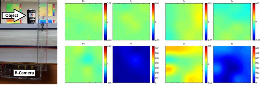
2

screen. We use a similar reconstruction and display subsystems
as in the B-Scanner; i.e, data collected by the sensor-array are
send to a PDU (processing and display unit); which can be
implemented on smartphones, tablets, or computers, through
a USB or a Bluetooth port.
   The rests of the paper are organized as follows. In Section
II, we briefly describe the principle of the proposed B-Camera.
The following Section III describes the experiments, including
the arrangement, reconstruction of image, and analysis of the
results. Section IV summarizes and concludes the paper.
                                                                    Fig. 1. A block diagram of the B-Camera showing its subsystems and
                                                                    their interactions. It consist of an Array of magnetometers and Multiplexer
                                                                    (implemented as an Arduino shield), a Microcontroller Unit (Arduino), a
               II. M ATERIALS AND M ETHODS                          Communication Unit (Bluetooth or USB port), and a Processing and Display
                                                                    Unit (implemented in a smartphone or a computer).
 A. B-Camera: A Magnetic Field Camera
   Human eyes cannot sense the presence of magnetic field.
To ”see” the magnetic field, one can use iron powder. By            into 4 × 4 array, so that the total size of the sensed area is
pouring the powder onto a sheet of paper which is placed            8 × 8 cm2 .
on a top of a magnet, we obtain a picture of magnetic field            The HMC5883L sensor can measure magnetic field up
lines. The flux density of the field is indicated by the density    to 8 gauss in three axis. The chip employs I2C (IC-to-IC
of the lines. More accurate measurement requires the use of a       Communication) protocol to communicate with other device,
magnetometer, which is usually brought around to scan an area       which in this case is a microcontroller. Since all of the
while the field values are recorded. The field distribution can     sensors have identical fixed address, we employed a 1-to-16
be derived by interpolating to locations within the surveyed        demultiplexer to access the field values of each sensor, which
area where the values are unknown. For an instantaneous             is controlled by four digital channels of the microcontroller.
display of the field—as required in a camera, an array of           This way, the measured field values can be read sequentially
magnetometers is necessary. In [14], a magnetic camera made         by the microcontroller from each sensor’s data registers.
of Hall-effect sensor has been proposed where magnetic field            2) Microcontroller Unit
strength of observed object are captured and displayed as a            The main tasks of the Microcontroller Unit are to read the
three-dimensional surface map.                                      sensors, to do a basic processing, and to send the result to the
   Additionally, we also cannot do focusing to a magnetic field,    PDU. We have employed an Arduino microcontroller because
which normally done in an optical camera by using a lens.           of its availability, affordability, and its openness. We read the
Therefore, the field is sensed directly at the corresponding        data through four digital channels of the microcontroller and
position by a magnetometer. The B-scanner in [1] operates           translate the integer (scaled) field values into a re-scaled proper
using a predefined grids over an observed area and measures         values in gauss unit. The results are then sent to PDU by using
the field at the center of each grid. Dividing the area into        a USB port, if the PDU is implemented on a computer, or by
grids are equivalent to discretization of the space, whereas        using a Bluetooth channel for the smartphone-based PDU.
the magnetometer of a smartphone in the B-Scanner also                  3) Communication Unit
gives discretized values of the magnetic field. Simultaneous           We can use either USB port or Bluetooth for communication
observation of the field values on the area can be obtained by      between the sensor array and the processing unit. When mo-
placing a number of sensors at the center of the grids, which       bility is prioritized, we can use a Bluetooth breakout such as
yields an array of magnetometers. At this point, there is a         the HC-06. The array data includes the ID of each sensor, the
close similarity between the B-Camera and an optical camera.        three components of measured magnetic fields {Bx , By , Bz },
                                                                    and a flag to indicate the end of a scan, so that the PDU can
                                                                    immediately process the data and display the image when all
 B. Construction of The B-Camera
                                                                    of the data in the array have already been received.
   In principle, the B-Camera works like the magnetic field             4) PDU (Processing and Display Unit)
scanner, unless the sensors position are fixed at a regular grid       The PDU can be implemented on either a computer or a
points/array. A block diagram displayed in Fig. 1 shows the         smartphone/tablet. Present days smartphones, despite of its
construction of the B-Camera.                                       affordability, have a sufficient computing power and display
    1) Sensor Array and Multiplexer                                 resolution to be used for this purpose. The main task of the
   The sensor-array performs spatial sampling of the magnetic       computing part is to interpolate the two-dimensional magnetic
field on an area, which is achieved by arranging the magne-         field values into a larger size. The purpose of interpolation
tometers into a two-dimensional array. The minimum spatial          is to present the user with a high-resolution image/video. We
sampling size, or the size of a sampling grid, will be related to   have implemented two interpolation algorithms in our device,
the dimension of the sensor. Since the present implementation       i.e. bilinear and bicubic [1], [15]. It has been coded in Java
uses a breakout of an HMC5883L magnetometer chip, we                using Android Studio for the smartphone based PDU and by
set the grid cell size to be 2 cm2 . The sensors are arranged       using Matlab for the computer based PDU.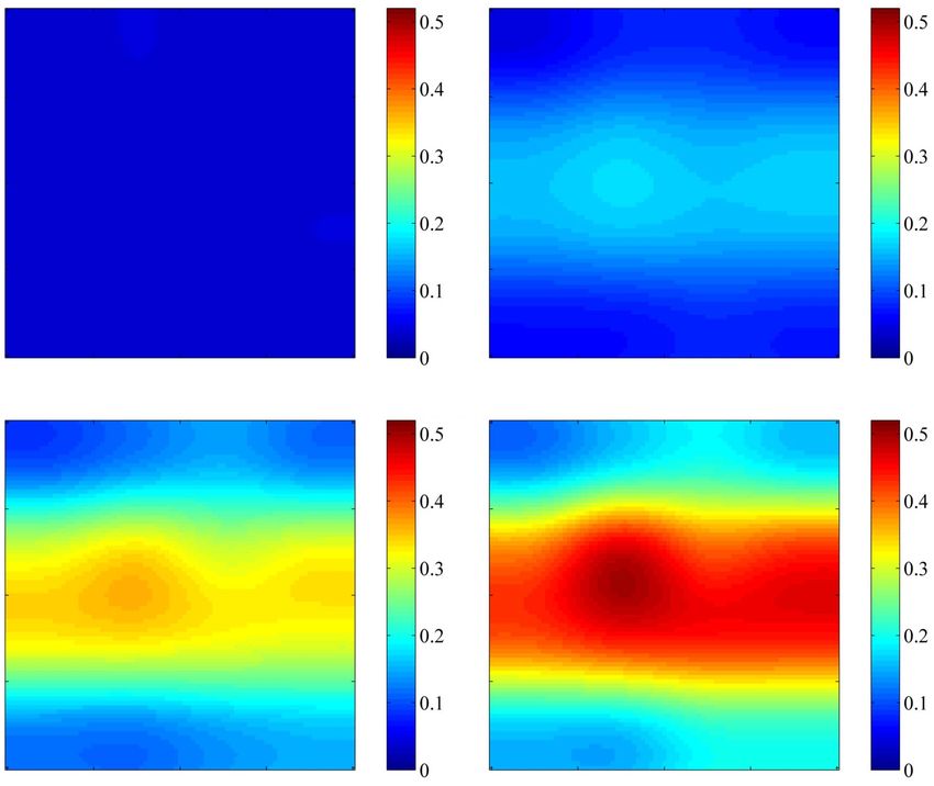
3

   The bilinear method requires four known values obtained by
measurements to estimate a field value at a particular point.
Based on these known values, the values on desired positions
are derived by using linear interpolation. The drawback of
the bilinear method is, when the sampling points are sparsely
distributed, the constructed field cannot be smoothly interpo-
lated. To obtain a better result, we can use bicubic method
that uses 16 neighboring values to estimate unknown values.
The interpolation is done by nonlinear function, therefore, a
smoother result can be obtained.
   The display unit shows magnetic field distribution for each
components and the total magnitude. For a given measured
field at a discrete point (m, n) within the surveyed area, where
m and n indicates the row and column number, respectively,
the vector of magnetic field is given by                                                                    (a)
      ~
      B(m, n) = Bx (m, n)î + By (m, n)ĵ + Bz (m, n)k̂      (1)
where î, ĵ, k̂ are unit vectors to the direction of x, y, and
z respectively. The magnitude of the magnetic flux density is
given by
                   q
     ~
    |B(m,   n)| = Bx2 (m, n) + By2 (m, n) + Bz2 (m, n)       (2)

Each of the components {Bx , By , Bz } and the magnitude |B|
are displayed separately by the PDU system. Observation of
field components is hardly possible in other imaging modali-
ties, such as radar and optical imaging. It enriches the features
which can increase recognition capability of the system.

             III. E XPERIMENTS AND A NALYSIS
                                                                                                           (b)
 A. Imaging A Coin with a Smartphone-Based PDU
   In this experiment, we have used the B-Camera with smart-        Fig. 2. Position of an object at B-Camera’s array and their corresponding
phone based PDU. The object was a nickel coin (Rp.1000),            magneto-photograph. The array is designed to be used downward, so that the
which possesses a ferromagnetic property. In the first experi-      left-right position of the image has been inverted. The object is a Rp.1000
                                                                    nickel coin: (a) it is positioned at the center of the the array, (b) it is located
ment, the coin was located at the center of the array, as shown     at the corner of the array. Images on at the right part of (a) and (b) shows
in the left part of Fig. 2(a). The magnitude field distribution     the consistency of the field distribution with their corresponding locations at
expressed in Eq.(2) was displayed on a smartphone screen            the left part.
shown in the right part of Fig.2(a). The image shows a circular
distribution of the field, which is strong at the center of the
array. This image is consistent with the position and shape of      was to show that a hidden object separated by a thick wall
the object.                                                         can be detected (and imaged) by the B-Camera.
   In the second experiment, the coin was located at the corner        Fig. 3 shows (a) experiment setting (test-range), (b) field
of the array. It should be noted that in a normal usage, the        distribution before an object was put, (c) field distribution after
array looks downward; therefore, the left-right positions are       the object has been placed on top of a book stack. The ruler in
exchanged. Left part of Fig. 2(b) shows the position of the         Fig. 3 (a) indicates that the distance between the sensor array to
object on the array, whereas the right part shows the field         the object is around 12 cm. By comparing the field distribution
distribution. This figure shows image of the object as expected,    without the object in Fig. 3 (a) with the one with an object
indicating that the device have worked properly.                    shown in Fig. 3 (b), we can see that the field has been changed
                                                                    and therefore the B-camera was capable to sense the field of
                                                                    an object located behind a thick wall. The colors represent the
 B. Observation of a Hidden Object
                                                                    field strength in gauss (G), whose values are indicated in the
  In this experiment, an object (a 9 V dry-cell battery) was        color bar.
located on a top of a book stack. We have used B-Camera
with a computer based PDU. The microcontroller (Arduino)
was connected to a USB port of the computer, where a Matlab           C. Imaging A Loaded Powerline Cable
program was running. By using the Matlab, we can obtain a              In this experiment, we have measured the magnetic field
better color contrast easily, which enhanced the display of the     induced by current in a loaded 50 Hz powerline cable. Since
magnetic field distribution. The purpose of this experiment         the cable (wire) was much longer than the length of the array,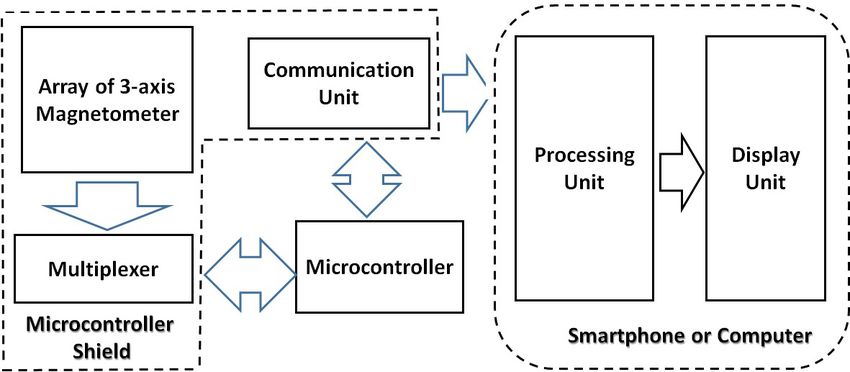
4
(a) (b) (c)
Fig. 3. Experiments to show the capability of the B-Camera to image a hidden object: (a) A dry-cell battery, whose cover is made of iron, is located on top
of a book stack to simulate a 12 cm wall hiding an object, (b) Magnetic field distribution with subtracted background without an object, (c) Field distribution
after the object has been put on top of the book stack. Color bar in (b) indicates magnetic field strength in gauss unit. By comparing figure (b) to (c), we
observe that the field distribution has changed. It shows that the device is capable to detect (and image) ferromagnetic objects hidden behind a thick wall.
~
the induced magnitude of magnetic field strength |B(m, n)| ≡
B(m, n) by a current I at an array sensor (m, n) located at a
distance r(m, n) from the center of the cable is given by
µ0 I
B(m, n) = (3)
2πr(m, n)
where µ0 is the permeability of the air (free space). The
field strength is proportional to the current I and inversely
proportional to the distance between the wire and the sensor.
Since the array is planar, whereas the cable is located above (a)
the center of the array, the field will be stronger at the center
of the array and weaker at the edge.
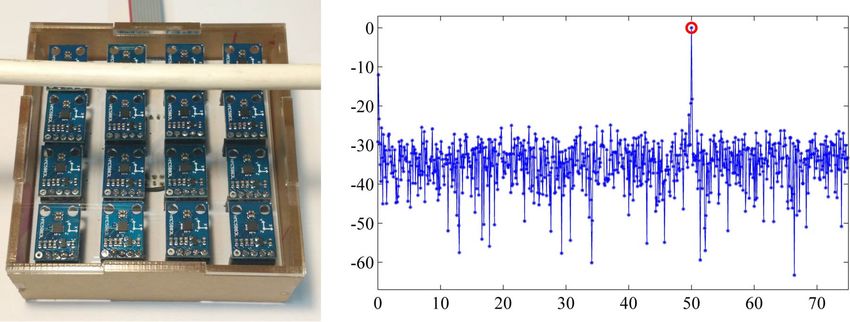
Fig. 4 shows (a) the experiment setup and spectrum of
the data, and (b) the observed results for various loads. The
sampling rate of the magnetometer is set to 150 Hz for all
field components. Spectrum of the original data displayed in
the right part of Fig. 4(a) shows a peak at 50 Hz. The collected
data were filtered, so that only the 50 Hz component of the
data were extracted.
Magnitude distribution of the magnetic fields for four loads,
i.e. 0 W, 25 W, 40 W, and 60 W incandescent lamps, are
displayed in Fig. 4(b). The figures shows that the flux density
increases with the increasing power dissipation of the loads,
which can be understood since for a given voltage V , the
current I is proportional to the power. We also observed that
the flux density is strong at the center and weaker at the edge
of the array. These results are consistent with Eq.(3).
IV. C ONCLUSIONS AND F URTHER D IRECTIONS
A magnetic field camera has been constructed. The array (b)
sensors are built from digital magnetometers, consisting of
4 × 4 elements. The camera has been demonstrated to map Fig. 4. Imaging a loaded 50 Hz powerline cable. (a) Left part shows the
the magnetic field distribution of ferromagnetic objects behind experiment setup where the cable is located around 3 cm from the B-Camera.
Right part shows the spectrum of the captured data. (b) Magnitude of magnetic
a surface, and to display the distribution at an instant time. flux density of the 50 Hz components: (upper left) when the cable is not
Additionally, the high sampling rate of the sensors also allows loaded, (upper right) with a 25 W load, (lower left) with a 40 W load, and
the camera to measure and map the distribution of magnetic (lower right) with a 60 W load.
field near a loaded 50 Hz powerline cable.
5

                        ACKNOWLEDGEMENTS
  This work has been supported by the ITB-Asahi Glass
Foundation Grant of Research 2018.

                               R EFERENCES
 [1] A.B.Suksmono, D. Danudirdjo, A. Setiawan, and D. Rahmawati, “Mag-
     netic subsurface imaging systems in a smartphone based on the built-in
     magnetometer,” IEEE Transactions on Magnetics, vol. 53, p. 3200405,
     2017.
 [2] J. Larmor, “Possible rotational origin of magnetic fields of sun and
     earth,” Electrical Review, vol. 85, p. 412, 1919.
 [3] N. Mariita, “The gravity method,” Short course II on surface exploration
     for geothermal resources, pp. 1–9, 2007.
 [4] A. Orozco, J. Gaudestad, N. E. Gagliolo, C. Rowlett, E. Wong, A. Jef-
     fers, B. Cheng, F. C. Wellstood, A. B. Cawthorne, and F. Infante, “3D
     magnetic field imaging for non-destructive fault isolation,” in Proc.
     ISTFA 2013, pp. 189–193, 2013.
 [5] L. A. Knauss, S. I. Woods, and A. Orozco, “Current imaging using mag-
     netic field sensors,” Microelectronics Failure Analysis Desk Reference,
     vol. 5, pp. 303–311, 2004.
 [6] R. McCary, D. Oliver, K. Silverstein, and J. Young, “Eddy current
     imaging,” IEEE Trans. Magn., vol. 20, no. 5, pp. 1986–1988, 1984.
 [7] K. Tsukada, T. Kiwa, T. Kawata, and Y. Ishihara, “Low-frequency
     eddy current imaging using MR sensor detecting tangential magnetic
     field components for nondestructive evaluation,” IEEE Transactions on
     Magnetics, vol. 42, no. 10, pp. 3315–3317, 2006.
 [8] M. Volk, S. Whitlock, C. H. Wolff, B. V. Hall, and A. I. Sidorov,
     “Scanning magnetoresistance microscopy of atom chips,” Rev. Sci.
     Instruments, p. 023702, 2008.
 [9] P. Y. Joubert, Y. L. Diraison, Z. Xi, and E. Vourc’h, “Pulsed eddy current
     imaging device for non destructive evaluation applications,” in Proc. of
     IEEE-SENSOR 2013, 2013.
[10] P.-Y. J. T.Bore, D. Placko, “Semi-analytical modeling of an eddy current
     imaging system for the characterization of defects in metallic structures,”
     in Proc. of IEEE-Sens. App. Symposium 2015, 2015.
[11] M. N. Baibich, J. M. Broto, A. Fert, F. N. V. Dau, F. Petroff, P. Etienne,
     G. Creuzet, A. Friederich, and J. Chazelas, “Giant magnetoresistance
     of (001)Fe/(001)Cr magnetic superlattices,” Phys. Rev. Lett., vol. 61,
     p. 2472, 1988.
[12] G. Binasch, P. Grunberg, F. Saurenbach, and W. Zinn, “Enhanced
     magnetoresistance in layered magnetic structures with antiferromagnetic
     interlayer exchange,” Phys. Rev. B, vol. 39, p. 4828(R), 2004.
[13] J. S. Moodera, L. R. Kinder, T. M. Wong, and R. Meservey, “Large
     magnetoresistance at room temperature in ferromagnetic thin film tunnel
     junctions,” Phys. Rev. Lett., vol. 16, pp. 3273–3276, 1995.
[14] B. A. Tuan, A. de Souza-Daw, T. M. Hoang, and N. T. Dzung, “Magnetic
     camera for visualizing magnetic fields of home appliances,” in Proc.
     IEEE-ICCE 2014, pp. 370–375, 2014.
[15] A.B.Suksmono, “Interpolation of PSF based on compressive sampling
     and its application in weak lensing survey,” Monthly Notices of the Royal
     Astronomical Society, vol. 443, pp. 919–926, 2014.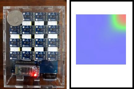
You can also read