A Silicon photonic Data Link with a Monolithic erbium-Doped Laser - Nature
←
→
Page content transcription
If your browser does not render page correctly, please read the page content below
www.nature.com/scientificreports

            OPEN           A Silicon Photonic Data Link with a
                           Monolithic Erbium-Doped Laser
                           Nanxi Li1,2,3, Ming Xin1, Zhan Su1,4, Emir Salih Magden1,5, Neetesh Singh1, Jelena Notaros1,
                           Erman Timurdogan1,4, Purnawirman Purnawirman1, Jonathan D. B. Bradley1,6 &
                           Michael R. Watts1*
                           To meet the increasing demand for data communication bandwidth and overcome the limits of
                           electrical interconnects, silicon photonic technology has been extensively studied, with various
                           photonics devices and optical links being demonstrated. All of the optical data links previously
                           demonstrated have used either heterogeneously integrated lasers or external laser sources. This work
                           presents the first silicon photonic data link using a monolithic rare-earth-ion-doped laser, a silicon
                           microdisk modulator, and a germanium photodetector integrated on a single chip. The fabrication is
                           CMOS compatible, demonstrating data transmission as a proof-of-concept at kHz speed level, and
                           potential data rate of more than 1 Gbps. This work provides a solution for the monolithic integration of
                           laser sources on the silicon photonic platform, which is fully compatible with the CMOS fabrication line,
                           and has potential applications such as free-space communication and integrated LIDAR.

                           With the increasing demand for data communication bandwidth, silicon photonic technology has been exten-
                           sively studied in integrated optical circuits to overcome the limits of electrical interconnects. Silicon is the mate-
                           rial of choice for both microelectronic circuits and integrated photonic components. The high refractive index
                           contrast between silicon and the silicon dioxide cladding enables highly compact photonic devices. Additionally,
                           the compatibility with the mature complementary-metal-oxide-semiconductor (CMOS) fabrication technol-
                           ogy allows for low-cost and high-volume production of silicon photonic devices, including large-scale phased
                           arrays1–3, low power modulators4,5, ultra-wideband multiplexers6, and waveguides for supercontinuum genera-
                           tion7,8. The demonstration of these devices makes silicon photonic an ideal platform for system-on-chip optical
                           interconnects.
                               Yet, all of the optical data links demonstrated so far used either heterogeneously integrated lasers9–11 or external
                           laser sources12–15. One of the main challenges in a true monolithic data link is the indirect bandgap of silicon, ren-
                           dering it unsuitable as a lasing medium. To overcome this problem, different approaches have been used to realize
                           laser sources on silicon, including heterogeneous integration or direct growth of III-V semiconductors16–18, stim-
                           ulated Raman emission in silicon19,20, germanium (Ge) and germanium-tin (GeSn)21–23, and rare-earth-doped
                           thin films24–28. Among these approaches, deposition of rare-earth-doped aluminum-oxide (Al2O3:RE3+) glass
                           as the gain medium29 has proven to be effective for advanced circuits on silicon, due to several key advantages.
                           First, the rare-earth-doped glass can be deposited on silicon wafers as a single-step back-end-of-line process30,
                           which enables monolithic, scalable integration and potential for low-cost high-volume mass production. Second,
                           rare-earth-ion-based lasers can provide narrow intrinsic linewidths since the optical pumping process intro-
                           duces no free carriers25,31–33. Furthermore, the low thermo-optic coefficient of the host medium (Al2O3) enables
                           laser operation over a wide temperature range34,35, important for control-free WDM systems36. Both erbium-
                           and thulium-doped lasers are able to achieve high optical output power37,38, which is able to meet the challeng-
                           ing power budget in LIDAR systems39,40 or ultrafast pulsed lasers41. Finally, common rare-earth materials, such
                           as erbium, thulium, and holmium, have wide emission spectra enabling large wavelength range coverage32,42–44
                           and the potential for short pulse generation through mode-locking26,45–49. In addition, the effectiveness of
                           rare-earth-doped lasers on silicon is further enhanced with the availability of compact un-cooled pump laser

                           1
                            Research Laboratory of Electronics, Massachusetts Institute of Technology, 77 Massachusetts Avenue, Cambridge,
                           MA, 02139, USA. 2John A. Paulson School of Engineering and Applied Science, Harvard University, 29 Oxford Street,
                           Cambridge, MA, 02138, USA. 3Present address: Institute of Microelectronics, Agency for Science, Technology and
                           Research (A*STAR), 2 Fusionopolis Way, Singapore, 138634, Singapore. 4Present address: Analog Photonics, 1
                           Marina Park Drive, Boston, MA, 02210, USA. 5Present address: Department of Electrical and Electronics Engineering,
                           Koç University, Sarıyer, İstanbul, 34450, Turkey. 6Present address: Department of Engineering Physics, McMaster
                           University, 1280 Main Street West, Hamilton, Ontario, L8S 4L7, Canada. *email: mwatts@mit.edu

Scientific Reports |   (2020) 10:1114 | https://doi.org/10.1038/s41598-020-57928-5                                                               1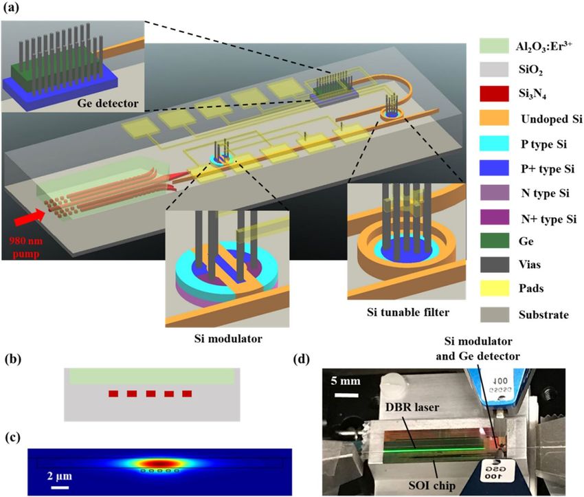
www.nature.com/scientificreports/                                                             www.nature.com/scientificreports

                           Figure 1. (a) Schematic of the photonics link, including the integrated erbium-doped laser, silicon microdisk
                           modulator, silicon microring tunable filter, and germanium (Ge) photodetector (drawing not to scale). (b)
                           Integrated erbium-doped distributed Bragg reflector (DBR) laser gain waveguide cross section. (c) The electric
                           field intensity of the fundamental mode for the DBR laser gain waveguide. (d) The fabricated system on the test
                           setup, showing green color fluorescence from the Al2O3:Er3+ laser waveguide excited by the 980 nm pump.

                           diodes50 and recent advances in photonics packaging51, which makes the co-package of the optical pump lasers
                           easy to implement and achieve system-level compactness. Hence, besides the advantage of providing narrow laser
                           linewidth, the advances in pump diode packaging offer compact solution for the optical pump to power several
                           rare-earth-doped lasers simultaneously.
                               Using CMOS-compatible fabrication methods, rare-earth-ion-based monolithically integrated lasers have
                           been demonstrated across near-infrared wavelengths at 1.0, 1.5, 1.8, 2.1 µm using ytterbium52,53, erbium25,27,54,
                           thulium37,55, and holmium56 doped Al2O3 glass as gain media, respectively. These lasers use silicon-nitride (Si3N4)
                           cavities, as Si3N4 has high transparency and low loss from near-IR to the mid-IR wavelength regime57,58. This
                           approach provides a mature wafer-scale waveguide platform for both passive and nonlinear silicon photonic
                           devices59–61. Nevertheless, the integration of rare-earth-ion-based lasers on a full silicon photonic platform
                           has proven to be challenging due to the added design and fabrication complexity, and the fact that the high
                           Al2O3:RE3+ deposition temperature tends to damage the active devices within the platform30. Up until now,
                           rare-earth-doped lasers on an active silicon-on-insulator (SOI) wafer platform, which enables integration of
                           lasers with active silicon photonic circuits, have only been recently demonstrated with an optical phased array39.
                           Such system demonstrated earlier has limited integration complexity without signal modulator and photodetec-
                           tor as receiver.
                               In this work, an optical data link using a monolithically integrated rare-earth-doped laser as a light source
                           on an SOI wafer is demonstrated for the first time. An erbium-doped distributed Bragg reflector (DBR) laser, a
                           silicon microdisk modulator and a Ge detector are monolithically integrated and used for signal generation, mod-
                           ulation and detection, respectively. By using a backend step for Al2O3:Er3+ deposition at an on-chip temperature
                           of 310 °C, we enabled CMOS-compatible fabrication of all the active and passive silicon photonic components
                           on a single chip. The system demonstrates data transmission as a proof-of-concept at kHz speed level, and the
                           potential data rate of more than 1 Gbps.

                           Results
                           Integrated system design. A schematic diagram of the system is shown in Fig. 1(a). It mainly consists of
                           four components: an erbium-doped DBR laser source, a silicon microdisk modulator, a silicon tunable filter, and
                           a Ge photodetector.
                               The waveguide cross section of the DBR laser is shown in Fig. 1(b). The width and gap of the Si3N4 pieces are
                           selected to be 450 nm and 400 nm, respectively, to provide large mode confinement factors for both the 980 nm

Scientific Reports |   (2020) 10:1114 | https://doi.org/10.1038/s41598-020-57928-5                                                          2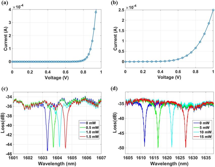
www.nature.com/scientificreports/                                                               www.nature.com/scientificreports

                           pump and 1560 nm laser signal modes within the Al2O3:Er3+ film. Figure 1(c) shows the fundamental transverse
                           electric (TE) mode intensity profile of the 1560 nm signal. The height of each Si3N4 piece is 200 nm. The gap
                           between the Si3N4 and Al2O3:Er3+ layer is 200 nm. A 1100-nm thick Al2O3:Er3+ film is deposited on top of the
                           chip to provide gain. The DBR cavity is formed by Si3N4 grating pieces on both sides of the laser gain waveguide,
                           with a duty cycle of 0.5 and a period of 493 nm. At the pump input, 4 side Si3N4 pieces in the gain waveguide
                           act as gratings to provide optical feedback at lasing wavelength, as shown in Fig. 1(a). At the signal output, the
                           widths of both leftmost and rightmost Si3N4 piece in the gain waveguide are reduced from 450 nm to 350 nm.
                           The periodic variation of the original and the reduced Si3N4 width forms grating and creates feedback for lasing
                           signal. The schematic is also illustrated in Fig. 1(a). The coupling coefficient (κ) is calculated to be 4.5 × 10³ m−1
                           and 5.7 × 10² m-1 at the pump input side and lasing signal output side respectively, in order to provide sufficient
                           feedback for lasing and reasonable signal power for output. The total length of the DBR laser is 2 cm, limited by
                           the maximum length of the chip. At the end of the DBR laser, a transition is designed to adiabatically couple the
                           mode from the DBR gain waveguide into the mode of a waveguide in the Si3N4 layer, with a waveguide width of
                           1.5 μm. At the end of Si3N4 waveguide, the mode is again adiabatically coupled into a waveguide in the silicon
                           layer, with a silicon width of 0.4 μm.
                               Once the laser mode is adiabatically coupled into the silicon waveguide, it is then evanescently coupled into a
                           silicon microdisk modulator, as shown in the enlarged area of Fig. 1(a). The modulator has a vertical p-n junction
                           with implants of different doping energies (similar to62,63). The modulator design is based on the existing compo-
                           nent reported earlier with minor modifications64, where the extinction ratio and the insertion loss of the silicon
                           microdisk modulator have been reported to be 5 dB and 1 dB, respectively. The vertical junction structure max-
                           imizes the overlap of the depletion region with the optical mode, minimizing the power consumption and drive
                           voltage. The modulator is contacted in the center of the disk using n+ and p+ implants and metal vias. Compared
                           with the ridge waveguide structure65, the contact of the vertical junction can be made from the interior of the res-
                           onator and hence enables a hard outer wall, which minimizes the radiation loss due to the tight bends in a small
                           diameter resonator. The structure further reduces the capacitance and the drive power of the modulator. The
                           microdisk has a radius of 3 μm, which gives a 38 nm free spectral range (FSR). Its electro-optic phase efficiency
                           Vπ·L is measured to be 0.61 V·cm. The microdisk modulator also has an integrated heater with interior contacts
                           that enables a thermal tuning range of 6 nm and efficiency of 0.86 nm/mW, in order to match the modulator’s
                           resonance with the lasing signal. A similar vertical junction microdisk modulator design reported earlier by our
                           group has a measured electro-optic 3 dB bandwidth of 21 GHz5.
                               After signal modulation, the optical mode is coupled back into the silicon waveguide, and transmitted to the
                           receiver side. A silicon microring filter (similar to32,66) is used to filter and couple the modulated signal into the
                           Ge detector. The filter acts as an essential component for reconfiguration of future optical communication net-
                           work on chip. The zoomed-in views of both the silicon microring tunable filter and the Ge detector are shown
                           in Fig. 1(a). For the tunable filter, an interior-ridge silicon resonator is selected, which introduces a relatively
                           thicker outer wall. The high index contrast at the outer wall enables tight bend of the waveguide without intro-
                           ducing large radiation loss. For tunability of this resonator, an embedded silicon heater is formed within the
                           ridge-etched region, using low- and high-dose p-type implants. The attachment of a silicon heater to the wave-
                           guide core directly heats the silicon in a thermally isolated environment (i.e. buried SiO2), achieving an efficient
                           thermal tuning of 1 nm/mW. The outer radius of the silicon microring is 3 μm, with an FSR of 35 nm. The position
                           of the doped regions is optimized for minimum absorption due to the embedded heater. The heater resistance is
                           reduced by forming the heater with multiple resistors that are connected in parallel to minimize the drive voltage.
                           The resonance of the tunable filter is thermally tuned to match the erbium-doped DBR laser signal wavelength,
                           select the modulated signal, and couple into the Ge detector.
                               The coupling from the silicon bus waveguide to Ge detector is achieved by an evanescent taper. This coupling
                           method uses mode evolution to transfer power into the Ge-on-Si region gradually and efficiently with longer
                           taper lengths enabling higher transmission67. The Ge is hetero-epitaxially grown into deep oxide trenches on
                           top of a body silicon layer, which is heavily p-doped. The body silicon layer is extended outside the Ge to be con-
                           tacted. The top of the Ge is implemented by a shallow n-type dopant and contacted directly, forming a vertical
                           p-i-n junction between the top of the Ge layer and the body silicon base layer. The Ge detector has a length of 12
                           μm and a width of 4 μm. The length is chosen to balance the trade-off between the coupler length and bandwidth.
                           The design is also based on the existing component reported earlier with minor modifications64,67, where the 3 dB
                           bandwidth is limited to 40 GHz and responsivity can reach 1 A/W at the designed working wavelength. The full
                           fabricated integrated system excited by a 980-nm laser diode pump is shown in Fig. 1(d). Green fluorescence
                           from the erbium-doped DBR laser waveguide can be observed. Optical pumping used here can provide better
                           linewidth without complex locking loops31,33.

                           System characterization and discussion.              It is known that post processing of the CMOS wafer beyond
                           400 °C can compromise the integrity of the metal contacts and vias. In order to find out the proper Al2O3:Er3+
                           thin film deposition temperature for our fabricated device, successive deposition iterations from high to low tem-
                           perature were conducted, until the current-voltage (I-V) characteristics of the modulator and Ge photodetector
                           still show the diode response after the deposition. Such temperature was found to be 310 °C on the substrate of
                           the device. More details about the substrate temperature measurement are provided in Supporting Information
                           section 1. To further prove the CMOS compatibility of the back-end-of-line Al2O3:Er3+ thin film deposition, the
                           I-V characteristics of the silicon microdisk modulator and the Ge detector after the deposition are compared
                           with the ones measured from the chip with the same device design and fabrication process before the gain film
                           deposition, showing insignificant degradation. The diode responses of the microdisk modulator and the Ge pho-
                           todetector after the deposition are presented in Fig. 2(a,b), respectively. Both demonstrate the expected diode
                           response after the deposition and confirm that the metal layer is not damaged by the thermal condition during

Scientific Reports |   (2020) 10:1114 | https://doi.org/10.1038/s41598-020-57928-5                                                             3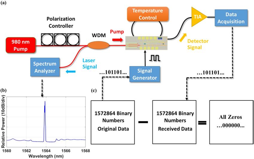
www.nature.com/scientificreports/                                                              www.nature.com/scientificreports

                           Figure 2. Current-voltage characteristics of the (a) vertical junction microdisk modulator and (b) Ge
                           photodetector, showing the diode responses. Thermal tuning of the (c) microdisk modulator and (d) microring
                           filter. Both diode responses and thermal tuning indicate working condition of the system after erbium-doped
                           Al2O3 thin film deposition at 310 °C.

                           the deposition. In addition, the thermal tuning of the microdisk modulator and microring filter for detector
                           are tested, as shown in Fig. 2(c,d), respectively. The thermal tuning efficiency of the microdisk modulator and
                           microring filter are measured to be 0.86 nm/mW and 1.0 nm/mW, respectively. Both I-V characteristics and the
                           thermal tuning demonstrated in Fig. 2 indicate that the system is still in working condition after the Al2O3:Er3+
                           thin film deposition at 310 °C.
                               Next, an external tunable laser source is used to obtain the passive response of the system. The tunable laser
                           source is used to sweep the wavelength of the input signal. A polarization controller is placed after the external
                           tunable laser source to ensure the input laser signal is coupled into the fundamental TE mode of the DBR laser
                           and silicon waveguide. An optical power meter is used to record the signals at the through port of the detector
                           microring filter. A thermoelectric cooler (TEC) is placed at the bottom of the chip to monitor and stabilize the
                           operating temperature of the system with a feedback loop. A cleaved single-mode HI1060 fiber is used on the
                           input side of the chip to butt-couple the tunable laser signal onto the chip, and a lensed fiber with 3-μm spot size
                           is used to couple out the output signal from the silicon taper at the other end of the chip. A drawing of the meas-
                           urement setup and more details are provided in Supporting Information section 3.
                               In Fig. 3(a), the resonances marked with red, green, and purple circles are the modulator, detector ring filter,
                           and DBR laser cavity resonances, respectively. The microdisk modulator has a higher total Q-factor than the
                           ring filter in design, therefore, exhibiting a narrower resonance than the microring filter connected to the pho-
                           todetector. One of the modulator resonances overlaps with the DBR laser cavity resonance, but does not exactly
                           match the laser wavelength. Thermal tuning is then used to match the DBR laser wavelength, the microdisk mod-
                           ulator resonance, and the detector ring filter resonance at 1564 nm, as shown in Fig. 3(b).
                               Following passive response measurement and resonance alignment, the active characterization of the system
                           is conducted using the setup shown in Fig. 4(a). A 980 nm pump source together with a polarization controller
                           is used to couple the pump signal into the fundamental TE mode of the laser gain waveguide. An external WDM
                           is used to filter out the lasing signal from the pump side of the DBR laser and an optical spectrum analyzer
                           (OSA) is used to monitor the signal from the DBR laser. The lasing spectrum is shown in Fig. 4(b), with more
                           than 30 dB side mode suppression ratio (SMSR). The lasing spectrum is recorded by the OSA with a wavelength
                           interval of 0.004 nm. A cleaved HI1060 fiber is used on the input side of the chip to butt-couple the pump onto the
                           chip, with launched pump power of 60 mW. The laser slope efficiency is estimated to be 0.02%, which is limited
                           by the reduced gain film depositon temperature and the roughness at the bottom of the gain waveguide. More
                           details about the laser efficiency improvements and system power budget are provided in Supporting Information

Scientific Reports |   (2020) 10:1114 | https://doi.org/10.1038/s41598-020-57928-5                                                           4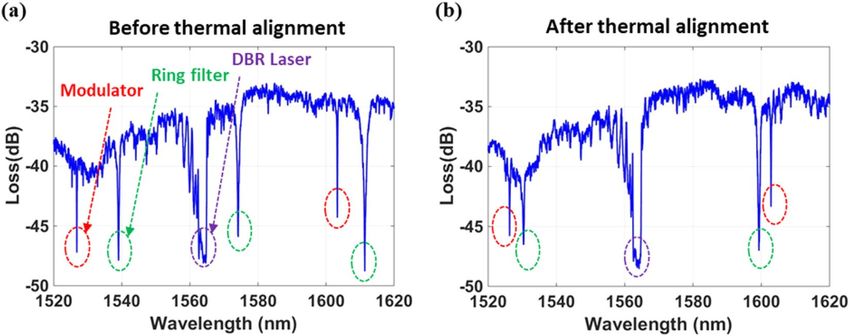
www.nature.com/scientificreports/                                                              www.nature.com/scientificreports

                           Figure 3. (a) Passive response of the link system showing the resonances of the microdisk modulator, detector
                           ring filter, and DBR laser marked in red, green, and purple dotted lines, respectively. (b) Passive response of the
                           link after thermal alignment of the resonances of the microdisk modulator, detector ring filter, and DBR laser.

                           Figure 4. (a) Active characterization setup including a 980 nm laser pump source together with a polarization
                           controller to ensure the fundamental TE mode is coupled into the Al2O3:Er3+ DBR laser, an OSA to monitor the
                           DBR laser output, a temperature control feedback loop to modify and monitor the temperature of the system,
                           and a TIA to amplify the electrical signal that is then monitored by the oscilloscope. (b) Optical spectrum of
                           the DBR laser recorded by the OSA, showing >30 dB SMSR. (c) The subtraction between the original binary
                           data for signal generator and the received binary data from Ge photodetector gives all zero, showing data
                           transmission without error bit.

                           section 4. The TEC is used to monitor the operating temperature of the system and stabilize the device temper-
                           ature by reducing the thermal shift due to the pump power. The electrical modulation signal is applied on the
                           silicon modulator through a high-speed probe. The modulated lasing signal then propagates through the silicon
                           waveguide and couples into the Ge photodetector through the microring filter. Another high-speed probe in con-
                           tact with the integrated Ge photodetector is used to collect the electrical signal. The photocurrent is sub-micro
                           ampere. In order to record the electrical signal from Ge detector, the collected photocurrent is amplified by an
                           off-chip trans-impedance amplifier (TIA) (SR570 low noise current preamplifier) and then read by a data acqui-
                           sition card.
                               Using the integrated data-link system, we demonstrate data transmission. The 1572864 binary numbers to
                           be transmitted are decoded from a color image. To avoid potential thermal drift on the silicon modulator from
                           consecutive “0” or consecutive “1” modulation voltages, each decoded binary number “0” and “1” are further

Scientific Reports |   (2020) 10:1114 | https://doi.org/10.1038/s41598-020-57928-5                                                           5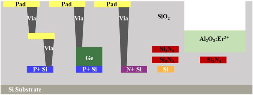
www.nature.com/scientificreports/ www.nature.com/scientificreports
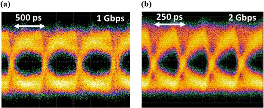
Figure 5. The eye pattern of the data link system (measured using an external laser source with the integrated
laser bypassed) under (a) 1 Gbps and (b) 2 Gbps data stream.
replaced by “01” and “10”, respectively. The generated 3145728 binary numbers are then converted into voltage
signals (-0.8 V for “0”, and 1 V for “1”) and applied to the silicon modulator to modulate the laser signal. At the Ge
photodetector, the received modulated signal is first collected by a National Instrument (NI) data acquisition card
(USB 6361) and then each two adjacent voltage signals are grouped into one pair. By comparing the relative volt-
age values of two signals, each pair can be easily converted into a binary number (“0” for “01” pattern and “1” for
“10” pattern). Finally, the original 1572864 binary numbers are subtracted by the received binary numbers, which
gives 1572864 zero numbers, demonstrating data transmission without error bit. The data transmission exper-
iment is conducted at kHz level speed as a proof-of-concept for the first monolithic silicon photonic data link.
The speed is mainly limited by the 1 MHz maximum bandwidth of the TIA. Based on the previous experimental
results of the silicon modulator and photodetector64,67, if the state-of-the-art TIA with GHz bandwidth can be
used here or the lasing power can be increased so as to reduce the TIA gain requirement, the signal transmission
with higher modulation frequency at GHz level can be readily demonstrated.
To analyze the potential high-speed capabilities of the system, we bypass the integrated laser and instead use
an external high power laser source to inject power from the input side of the link. For this experiment, instead of
using an Al2O3:Er3+ gain film, an undoped Al2O3 thin film is deposited on the chip with the same design to form
the passive laser waveguide without signal absorption from the erbium ions. The experimental setup is provided
in Fig. S4 of the Supporting Information. A laser source cascaded with a high-power erbium-doped fiber ampli-
fier (EDFA) is used as an external source to provide the laser signal at the wavelength matching with the reso-
nances of the silicon microdisk as well as the microring filter. The amplified laser signal is butt-coupled onto the
chip through a cleaved HI1060 fiber, with an estimated on-chip power of 136 mW, which we have demonstrated
using similar rare-earth-doped waveguide laser structures37. Such power is required, based on the system loss
budget provided in Supporting Information section 4, for the Ge detector to generate enough photocurrent for
later analysis without using a TIA. A pattern generator is used to provide 1 or 2 Gbps level pseudorandom binary
sequence (PRBS) signal to the silicon modulator. A sampling scope is connected to the Ge detector through a
bias tee to capture the eye diagram, as shown in Fig. 5(a,b). We observe open eye patterns at 1 and 2 Gbps. As the
frequency of the PRBS is increased beyond 3 Gbps, the “eye” becomes unclear, which might be contributed by
the loss from the mode transitions and the microring structures. The future work to improve the power budget
within the system includes the optimization of the wafer-level laser trench fabrication process, the design for the
waveguide transitions, the gain film deposition and the laser cavity design. More details about the high-speed
characterization setup and the system loss budget are provided in Supporting Information section 3 and 4 respec-
tively. The speed of this proof-of-concept system can be improved by reducing the system loss and increasing the
power coupled into the photodetector.
Conclusions
In conclusion, we have demonstrated a single-chip optical data link on an SOI wafer fabricated in a standard
CMOS foundry. An erbium-doped DBR laser is monolithically integrated as the light source. A reverse-biased
vertical junction microdisk modulator is used to modulate the signal. A silicon tunable microring filter is
designed to pick up the modulated signal, and a Ge photodetector is used to capture the transmitted signal.
The functionality of the datalink is demonstrated by data transmission as a proof-of-concept at kHz speed level.
Modulation and signal transmission results are shown with potential for high-speed operation of more than
1 Gbps. These results pave the way for monolithic integration of amplifiers and lasers, potentially for free-space
communication and many other applications on a full silicon photonic platform.
Scientific Reports | (2020) 10:1114 | https://doi.org/10.1038/s41598-020-57928-5 6www.nature.com/scientificreports/ www.nature.com/scientificreports
Figure 6. Simplified diagram illustrating the silicon photonic platform utilized for the link system. The
platform includes two Si3N4 layers, a silicon layer with different doping levels, two metal layers, two via layers, a
Ge layer for the photodetector, and a trench for deposition of the erbium-doped Al2O3 thin film.
Methods
Fabrication process. The wafer-level fabrication process (except the Al2O3:Er3+ thin film deposition) is done
in a state-of-the-art CMOS foundry at the Colleges of Nanoscale Science and Engineering, SUNY Polytechnic
Institute in Albany, NY. The platform consists of two Si3N4 layers, a silicon layer with different doping levels, two
metal layers, two via layers, a Ge layer for the photodetector, and a trench for deposition of an erbium-doped
Al2O3 thin film. Figure 6 shows a simplified schematic of the layers in this silicon photonic platform. The top
copper metal layer is for routing and contact pads. A copper via is used between the top and bottom metal layers.
The bottom copper metal layer is for routing. A bottom via is for contact to the bottom silicon layer. The CMOS
foundry uses 193 nm immersion lithography on a 300-mm-diameter SOI wafer with 220 nm silicon height and
2-µm thick buried oxide. The Ge layer is hetero-epitaxially grown on top of a heavily p-doped silicon base. An
n-type dopant is implanted at the top of the Ge to form a vertical p-i-n junction for the detector. The vias are used
to connect the n-doped Ge and p-doped silicon together with metal contact pads. Two 200-nm-thick Si3N4 layers
are deposited using a plasma-enhanced chemical vapor deposition process, polished using a top surface polishing
process to reduce optical scattering loss, and patterned using 193 nm immersion lithography (this bottom-up
process distinguishes from the top-down etching processes68). The bottom Si3N4 layer defines the grating and
DBR cavity for the erbium-doped laser. A 4-µm-thick silicon dioxide layer is deposited above the top Si3N4, and
a 4-µm-deep trench for deposition of the gain media is etched into the silicon dioxide using the top nitride layer
as an etch stop.
After the wafer-level fabrication, the wafer is diced and the back-end-of-line deposition of the gain film is
performed on the chip level. A nominally 1100-nm-thick erbium-doped Al2O3 film is deposited on top of the
chip via reactive co-sputtering, at an on-chip temperature of 310 °C. The film thickness and doping energy are
optimized to ensure efficient lasing. The Er3+ doping concentration level is estimated to be 1.5 × 1020 cm−3. Under
lower doping level the lasing power will decrease due to the reduced gain, while under higher doping level the
lasing power will also decrease due to the clustering of the doping ion69,70. More details about the Al2O3 thin film
deposition are provided in Supporting Information section 1.
Numerical simulation. Effective indices and guided modes are simulated using a vector finite-difference 2D
eigenmode solver, with a discretization of 20 nm. The code is written in Matlab, and it solves the wave equation
of the transverse electric field at the signal wavelength. The refractive indices for Al2O3, Si3N4, and SiO2 are 1.649,
1.950, and 1.444, respectively. More detail on the simulation is provided in Supporting Information section 2 and
the mode solver code can be found in the appendix of71.
Received: 29 August 2019; Accepted: 7 January 2020;
Published: xx xx xxxx
References
1. Sun, J., Timurdogan, E., Yaacobi, A., Hosseini, E. S. & Watts, M. R. Large-scale nanophotonic phased array. Nature 493, 195 (2013).
2. Hajimiri, A., Hashemi, H., Natarajan, A., Xiang, G. & Komijani, A. Integrated Phased Array Systems in Silicon. Proc. IEEE 93,
1637–1655 (2005).
3. Poulton, C. V. et al. Large-scale silicon nitride nanophotonic phased arrays at infrared and visible wavelengths. Opt. Lett. 42, 21–24
(2017).
4. Manipatruni, S., Preston, K., Chen, L. & Lipson, M. Ultra-low voltage, ultra-small mode volume silicon microring modulator. Opt.
Express 18, 18235–18242 (2010).
5. Timurdogan, E. et al. An ultralow power athermal silicon modulator. Nat. Commun. 5, 4008 (2014).
6. Magden, E. S. et al. Transmissive silicon photonic dichroic filters with spectrally selective waveguides. Nat. Commun. 9, 3009 (2018).
7. Castelló-Lurbe, D. & Silvestre, E. Supercontinuum generation in silicon waveguides relying on wave-breaking. Opt. Express 23,
25462–25473 (2015).
8. Singh, N. et al. Octave-spanning coherent supercontinuum generation in silicon on insulator from 1.06 μm to beyond 2.4 μm. Light
Sci. Appl. 7, 17131 (2018).
9. Ohira, K. et al. On-chip optical interconnection by using integrated III-V laser diode and photodetector with silicon waveguide. Opt.
Express 18, 15440–15447 (2010).
10. Liu, H. F. Integrated silicon photonics links for high bandwidth data transportation. Optical Fiber Communication Conference 2014.
p. Th1D.1.
Scientific Reports | (2020) 10:1114 | https://doi.org/10.1038/s41598-020-57928-5 7www.nature.com/scientificreports/ www.nature.com/scientificreports
11. Gasse, K. V. et al. III-V-on-Silicon Photonic Transceivers for Radio-over-Fiber links. J. Lightwave Technol. 36, 4438–4444 (2018).
12. Buckwalter, J. F., Zheng, X., Li, G., Raj, K. & Krishnamoorthy, A. V. A Monolithic 25-Gb/s Transceiver With Photonic Ring
Modulators and Ge Detectors in a 130-nm CMOS SOI. Process. IEEE J. Solid State Circuits 47, 1309–1322 (2012).
13. Sun, C. et al. Single-chip microprocessor that communicates directly using light. Nature 528, 534–538 (2015).
14. Atabaki, A. H. et al. Integrating photonics with silicon nanoelectronics for the next generation of systems on a chip. Nature 556,
349–354 (2018).
15. Li, C. et al. Silicon Photonic Transceiver Circuits With Microring Resonator Bias-Based Wavelength Stabilization in 65 nm CMOS.
IEEE J. Solid State Circuits 49, 1419–1436 (2014).
16. Fang, A. W. et al. A Distributed Bragg Reflector Silicon Evanescent Laser. IEEE Photon. Tech. Lett. 20, 1667–1669 (2008).
17. Fang, A. W., Lively, E., Kuo, Y.-H., Liang, D. & Bowers, J. E. A distributed feedback silicon evanescent laser. Opt. Express 16,
4413–4419 (2008).
18. Chen, S. et al. Electrically pumped continuous-wave III–V quantum dot lasers on silicon. Nat. Photon. 10, 307–311 (2016).
19. Rong, H. et al. A continuous-wave Raman silicon laser. Nature 433, 725–728 (2005).
20. Boyraz, O. & Jalali, B. Demonstration of a silicon Raman laser. Opt. Express 12, 5269–5273 (2004).
21. Liu, J., Sun, X., Camacho-Aguilera, R., Kimerling, L. C. & Michel, J. Ge-on-Si laser operating at room temperature. Opt. Lett. 35,
679–681 (2010).
22. Al-Kabi, S. et al. An optically pumped 2.5 μm GeSn laser on Si operating at 110 K. Appl. Phys. Lett. 109, 171105 (2016).
23. Wirths, S. et al. Direct bandgap GeSn microdisk lasers at 2.5 μm for monolithic integration on Si-platform. 2015 IEEE International
Electron Devices Meeting (IEDM). 2.6.1-2.6.4.
24. M. Xin, et al. Optical frequency synthesizer with an integrated erbium tunable laser. Light Sci. Appl. 8, 122 (2019).
25. Belt, M. et al. Arrayed narrow linewidth erbium-doped waveguide-distributed feedback lasers on an ultra-low-loss silicon-nitride
platform. Opt. Lett. 38, 4825–4828 (2013).
26. Sorace-Agaskar, C. M. et al. Integrated mode-locked lasers in a CMOS-compatible silicon photonic platform. CLEO: Science and
Innovations, 2015, p. SM2I. 5.
27. Belt, M. & Blumenthal, D. J. Erbium-doped waveguide DBR and DFB laser arrays integrated within an ultra-low-loss Si3N4
platform. Opt. Express 22, 10655–10660 (2014).
28. Singh, G. et al. Resonant pumped erbium-doped waveguide lasers using distributed Bragg reflector cavities. Opt. Lett. 41, 1189–1192
(2016).
29. Worhoff, K. et al. Reliable Low-Cost Fabrication of Low-Loss Al2O3:Er3+ Waveguides With 5.4-dB Optical Gain. IEEE J. Quant.
Electron. 45, 454–461 (2009).
30. Magden, E. S. et al. Monolithically-integrated distributed feedback laser compatible with CMOS processing. Opt. Express 25,
18058–18065 (2017).
31. Bernhardi, E. H. et al. Ultra-narrow-linewidth, single-frequency distributed feedback waveguide laser in Al2O3:Er3+ on silicon.
Opt. Lett. 35, 2394–2396 (2010).
32. Li, N. et al. C-band swept wavelength erbium-doped fiber laser with a high-Q tunableinterior-ridge silicon microring cavity. Opt.
Express 24, 22741–22748 (2016).
33. Purnawirman et al. Ultra-narrow-linewidth Al2O3:Er3+ lasers with a wavelength-insensitive waveguide design on a wafer-scale
silicon nitride platform. Opt. Express 25, 13705–13713 (2017).
34. Purnawirman et al. Wavelength division multiplexed light source monolithically integrated on a silicon photonics platform. Opt.
Lett. 42, 1772–1775 (2017).
35. Belt, M. & Blumenthal, D. J. High temperature operation of an integrated erbium-doped DBR laser on an ultra-low-loss Si3N4
platform. Optical Fiber Communications Conference and Exhibition (OFC) 2015. p. Tu2C.7.
36. Li, N. et al. Athermal synchronization of laser source with WDM filter in a silicon photonics platform. Appl. Phys. Lett. 110,
211105 (2017).
37. Li, N. et al. High-power thulium lasers on a silicon photonics platform. Opt. Lett. 42, 1181–1184 (2017).
38. Hosseini, E. S. et al. CMOS-compatible 75mW erbium-doped distributed feedback laser. Opt. Lett. 39, 3106–3109 (2014).
39. Notaros, J. et al. CMOS-Compatible Optical Phased Arrays with Monolithically-Integrated Erbium Lasers. Conference on Lasers and
Electro-Optics (CLEO), San Jose, California, 2018, p. STu4B.2.
40. Guo, W. et al. Two-Dimensional Optical Beam Steering With InP-Based Photonic Integrated Circuits. IEEE J. Sel. Top. Quant.
Electron. 19, 6100212–6100212 (2013).
41. Kaertner, F. X. et al. Integrated rare-Earth doped mode-locked lasers on a CMOS platform. SPIE Photonics Europe, 10686–10614
(SPIE, Strasbourg, France, 2018).
42. Liu, Y. et al. Regenerative Er-doped fiber amplifier system for high-repetition-rate optical pulses. J. Opt. Soc. Korea 17, 357–361
(2013).
43. Simakov, N., Hemming, A., Clarkson, W. A., Haub, J. & Carter, A. A cladding-pumped, tunable holmium doped fiber laser. Opt.
Express 21, 28415–28422 (2013).
44. Li, N. et al. Monolithically integrated erbium-doped tunable laser on a CMOS-compatible silicon photonics platform. Opt. Express
26, 16200–16211 (2018).
45. Callahan, P. T. et al. Fully-Integrated CMOS-Compatible Q-Switched Laser at 1.9µm Using Thulium-Doped Al2O3. Conference on
Lasers and Electro-Optics (CLEO), San Jose, California, 2017, p. STh3N. 2.
46. Wong, J. H. et al. Photonic Generation of Frequency-Tunable Microwave Signals Using an Array of Uniformly Spaced Optical
Combs. J. Lightwave Technol. 30, 3164–3172 (2012).
47. Li, P., Ruehl, A., Grosse-Wortmann, U. & Hartl, I. Sub-100 fs passively mode-locked holmium-doped fiber oscillator operating at
2.06 µm. Opt. Lett. 39, 6859–6862 (2014).
48. Shtyrkova, K. et al. Integrated CMOS-compatible Q-switched mode-locked lasers at 1900nm with an on-chip artificial saturable
absorber. Opt. Express 27, 3542–3556 (2019).
49. Li, N. et al. Cavity-length optimization for high energy pulse generation in a long cavity passively mode-locked all-fiber ring laser.
Appl. Opt. 51, 3726–3730 (2012).
50. LUMENTUM. Ultra-Small Form Factor Pump Lasers, https://www.lumentum.com/en/products/200-mw-uncooled-980-nm-pump-
modules
51. Barwicz, T. et al. A Novel Approach to Photonic Packaging Leveraging Existing High-Throughput Microelectronic Facilities. IEEE
J. Sel. Top. Quant. Electron. 22, 455–466 (2016).
52. Su, Z. et al. Ultra-Compact CMOS-Compatible Ytterbium Microlaser. Advanced Photonics 2016 (IPR, NOMA, Sensors, Networks,
SPPCom, SOF). p. IW1A.3.
53. van Emmerik, C. I. et al. Single-layer active-passive Al2O3 photonic integration platform. Opt. Mater. Express 8, 3049–3054 (2018).
54. Purnawirman et al. Reliable Integrated Photonic Light Sources Using Curved Al2O3:Er3+ Distributed Feedback Lasers. IEEE
Photonics J. 9, 1–9 (2017).
55. Su, Z. et al. Ultra-compact and low-threshold thulium microcavity lasermonolithically integrated on silicon. Opt. Lett. 41,
5708–5711 (2016).
56. Li, N. et al. Broadband 2-µm emission on silicon chips: monolithically integrated Holmium lasers. Opt. Express 26, 2220–2230
(2018).
Scientific Reports | (2020) 10:1114 | https://doi.org/10.1038/s41598-020-57928-5 8www.nature.com/scientificreports/ www.nature.com/scientificreports
57. Sherwood-Droz, N. & Lipson, M. Scalable 3D dense integration of photonics on bulk silicon. Opt. Express 19, 17758–17765 (2011).
58. Huang, Y., Song, J., Luo, X., Liow, T.-Y. & Lo, G.-Q. CMOS compatible monolithic multi-layer Si3N4-on-SOI platform for low-loss
high performance silicon photonics dense integration. Opt. Express 22, 21859–21865 (2014).
59. Su, Z. et al. High-Q-factor Al2O3 micro-trench cavities integrated with silicon nitride waveguides on silicon. Opt. Express 26,
11161–11170 (2018).
60. Mu, J., de Goede, M., Dijkstra, M. & García-Blanco, S. M. Monolithic Integration of Al2O3 and Si3N4 for Double-layer Integrated
Photonic Chips. Advanced Photonics 2018 (BGPP, IPR, NP, NOMA, Sensors, Networks, SPPCom, SOF). p. ITh1I.1.
61. Frankis, H. C. et al. Four-Wave Mixing in a High-Q Aluminum Oxide Microcavity on Silicon. Conference on Lasers and Electro-
Optics (CLEO), San Jose, California, 2018. p. STh3I.3.
62. Timurdogan, E. et al. Vertical Junction Silicon Microdisk Modulator with Integrated Thermal Tuner. Conference on Lasers and
Electro-Optics (CLEO), San Jose, California, 2013. p. CTu2F.2.
63. Watts, M. R., Zortman, W. A., Trotter, D. C., Young, R. W. & Lentine, A. L. Vertical junction silicon microdisk modulators and
switches. Opt. Express 19, 21989–22003 (2011).
64. Timurdogan, E. et al. An Ultra Low Power 3D Integrated Intra-Chip Silicon Electronic-Photonic Link. Optical Fiber Communication
Conference Post Deadline Papers 2015. Th5B.8.
65. Xu, Q., Schmidt, B., Pradhan, S. & Lipson, M. Micrometre-scale silicon electro-optic modulator. Nature 435, 325–327 (2005).
66. Timurdogan, E. et al. A High-Q Tunable Interior-Ridge Microring Filter. Conference on Lasers and Electro-Optics (CLEO), San Jose,
California, 2014. p. SF2O.3.
67. Byrd, M. J. et al. Mode-evolution-based coupler for high saturation power Ge-on-Si photodetectors. Opt. Lett. 42, 851–854 (2017).
68. Wang, L. et al. Few-Layer Mxene Ti3C2Tx (T = F, O, Or OH) for Robust Pulse Generation in a Compact Er-Doped Fiber Laser.
ChemNanoMat 5, 1233–1238 (2019).
69. Li, N. et al. Self-pulsing in Erbium-doped fiber laser. 2015 Optoelectronics Global Conference (OGC) (2015), pp. 1-2.
70. Agazzi, L., Wörhoff, K. & Pollnau, M. Energy-Transfer-Upconversion Models, Their Applicability and Breakdown in the Presence of
Spectroscopically Distinct Ion Classes: A Case Study in Amorphous Al2O3:Er3+. The Journal of Physical Chemistry C 117,
6759–6776 (2013).
71. Li, N., Rare-Earth-Doped Lasers on Silicon Photonics Platforms, Ph.D. Thesis, Harvard University, Cambridge (2018).
Acknowledgements
The authors would like to acknowledge Gary Riggott and Kurt Broderick for assistance on Erbium-doped thin-
film deposition. This work is supported by Defense Advanced Research Projects Agency (DARPA) Electronic-
Photonic Heterogeneous Integration (E-PHI) project (HR0011-12-2-0007). N. Li is sponsored by National
Science Scholarship (NSS) from the Agency of Science, Technology and Research (A*STAR), Singapore.
Author contributions
N. L. performed the gain film deposition on the platform, characterized the device, analyzed the results, and wrote
the manuscript. M. X. conducted the data transmission experiment. Z. S., E. T. and P. P. designed the components
and laid out the mask. E. S. M. assisted on the fabrication. N. S. and J. N. assisted on the result analysis. J. D. B. B.
and M. R. W. supervised the project. All authors edited and revised the manuscript.
Competing interests
The authors declare no competing interests.
Additional information
Supplementary information is available for this paper at https://doi.org/10.1038/s41598-020-57928-5.
Correspondence and requests for materials should be addressed to M.R.W.
Reprints and permissions information is available at www.nature.com/reprints.
Publisher’s note Springer Nature remains neutral with regard to jurisdictional claims in published maps and
institutional affiliations.
Open Access This article is licensed under a Creative Commons Attribution 4.0 International
License, which permits use, sharing, adaptation, distribution and reproduction in any medium or
format, as long as you give appropriate credit to the original author(s) and the source, provide a link to the Cre-
ative Commons license, and indicate if changes were made. The images or other third party material in this
article are included in the article’s Creative Commons license, unless indicated otherwise in a credit line to the
material. If material is not included in the article’s Creative Commons license and your intended use is not per-
mitted by statutory regulation or exceeds the permitted use, you will need to obtain permission directly from the
copyright holder. To view a copy of this license, visit http://creativecommons.org/licenses/by/4.0/.
© The Author(s) 2020
Scientific Reports | (2020) 10:1114 | https://doi.org/10.1038/s41598-020-57928-5 9You can also read