AN12364 NTAG 5 - Bidirectional data exchange Rev. 1.0 - 9 January 2020 530310 - NXP Semiconductors
←
→
Page content transcription
If your browser does not render page correctly, please read the page content below
AN12364
  NTAG 5 - Bidirectional data exchange
  Rev. 1.0 — 9 January 2020                                         Application note
  530310                                                          COMPANY PUBLIC

Document information
Information     Content
Keywords        Data transfer, SRAM, PHDC, arbitration
Abstract        How to transfer data, Pass-through, SRAM, PHDC, memory arbitration
NXP Semiconductors
                                                                                                                       AN12364
                                                                                                     NTAG 5 - Bidirectional data exchange

Revision history
Rev           Date       Description
v.1.0         20200109   First official released version

AN12364                         All information provided in this document is subject to legal disclaimers.              © NXP B.V. 2020. All rights reserved.

Application note                             Rev. 1.0 — 9 January 2020
COMPANY PUBLIC                                         530310                                                                                       2 / 20
NXP Semiconductors
AN12364
NTAG 5 - Bidirectional data exchange
1 Abbreviations
Table 1. Abbreviations
Acronym Description
EEPROM Electrically Erasable Programmable Read-Only Memory
GPIO General-purpose input/output
2
I C Inter-Integrated Circuit
NFC Near field communication
PHDC Personal Health Device Communication
POR Power On Reset
PWM Pulse width modulation
RF radio frequency
SRAM Static random-access memory
AN12364 All information provided in this document is subject to legal disclaimers. © NXP B.V. 2020. All rights reserved.
Application note Rev. 1.0 — 9 January 2020
COMPANY PUBLIC 530310 3 / 20NXP Semiconductors
AN12364
NTAG 5 - Bidirectional data exchange
2 Introduction
NTAG 5 offers many ways for bidirectional data exchange. One of it is the "pass-through
mode", which allows the NTAG 5 to be used for bidirectional data transfer from an NFC
2
device to an I C-bus Host (e.g. a microcontroller).
The pass-through mode provides the SRAM for data communication and triggering
mechanisms for the synchronization of the data transfer.
2.1 Potential applications
• Read out of data collected in an embedded device (logging data)
• Upload new data in the embedded device (e.g. firmware update of the microcontroller)
• Bidirectional communication with exchange of commands and data (e.g. execute
functions in the microcontroller or execute authentication schemes)
AN12364 All information provided in this document is subject to legal disclaimers. © NXP B.V. 2020. All rights reserved.
Application note Rev. 1.0 — 9 January 2020
COMPANY PUBLIC 530310 4 / 20NXP Semiconductors
AN12364
NTAG 5 - Bidirectional data exchange
3 Interface Arbitration for memory access
2
Interface Arbitration logic is provided to give access to RF interface and I C interface
to access memory, without collisions. Two session register bits are provided to
indicate which interface booted up successfully and it is available: RF_BOOT_OK and
VCC_BOOT_OK.
Note: Tag can be "externally powered" by itself using energy harvesting, if VOUT and VCC
are shorted.
Memory consist of EEPROM, SRAM and Session registers. SRAM is available only when
tag is supplied by VCC (VCC_SUPPLY_OK = 1b) and SRAM_ENABLE configuration bit is
set to 1b. EEPROM and Session register are available when any of the supply sources is
available.
2 2
Arbitration mode is applicable for I C slave use case mode only. For I C Master and
GPIO/PWM use cases, no memory arbitration is done / needed.
There are four (4) arbitration schemes:
1. Normal mode [Section 4]
2. SRAM Mirror mode [Section 5] - shall be used when frequently changing data
is passed over NDEF message. E.g., Host is reading temperature from temp.
sensor and writing the value to the NTAG 5 User Memory Area, at the end of
NDEF URL every 0.5 s, like: http://www.desireddomainwithSensorData.com/
temp=023344&t1=25C. While SRAM provides unlimited write endurance, SRAM
Mirror is better to use instead of writing to EEPROM. So host would be writing
temperature to SRAM instead of EEPROM. Arbiter takes care that only one interface
access the SRAM at the time.
3. SRAM Pass-through mode [Section 6] - for bulk data exchange (up to 256 B in one
pass). Usually Host ↔ NTAG 5 ↔ NFC.
4. PHDC mode [Section 7] - for data exchange with Personal Health Care Device (e.g.
blood pressure device, body temperature measurement device). SRAM Mirror on the
first pages of User Memory is used for bulk data exchange, with help of arbitration
mechanism.
Also [TNEP] mode is supported.
Note: NFC Forum defined TNEP is used where no special arbitration is needed on IC
level.
AN12364 All information provided in this document is subject to legal disclaimers. © NXP B.V. 2020. All rights reserved.
Application note Rev. 1.0 — 9 January 2020
COMPANY PUBLIC 530310 5 / 20NXP Semiconductors
AN12364
NTAG 5 - Bidirectional data exchange
4 Normal Mode
ARBITER_MODE [1:0] = 00b indicates normal mode. Memory is accessible by both the
interfaces by “First come first serve” principle.
2
The arbiter locks to I C interface in following occasions:
2
• If the NTAG 5 is correctly addressed for the memory access on the I C interface, then
2
set I C_IF_LOCKED = 1b if NFC_IF_LOCKED = 1b.
2 2
• If I C_IF_LOCKED = 1b then I C interface can access EEPROM and SRAM.
• RF reader can access (read/write) the NTAG 5 status registers via RF commands at
any time. Any RF commands accessing EEPROM/CONFIGURATION memory will be
returned with NAK.
2
I C_IF_LOCKED will be cleared if
2
• I C host writes to clear the register bit.
• If this is not done by the host, this bit will be automatically reset to 0 if Watch Dog Timer
expires.
• At POR (all power sources).
2
• If I C supply switches off.
Note: If Watchdog timer is disabled, bit will not be cleared until transactions ends.
The arbiter locks to RF interface:
• If the NTAG 5 receives valid RF command and correctly addressed for memory access,
2
then set NFC_IF_LOCKED = 1b if I C_IF_LOCKED = 1b.
• If NFC_IF_LOCKED = 1b then RF interface can access NTAG 5 memory.
2 2 2
• I C host can access (read/write) the TAG status registers via I C commands. Any I C
commands to access memory will be returned with data NAK.
NFC_IF_LOCKED will be cleared automatically after:
• Completion of current valid RF command.
• At POR (all power sources).
• If RF field is switched OFF.
In Normal mode SRAM can be made available as part of memory or can disabled by
configuring SRAM_ENABLE bit.
If NTAG 5 is VCC supplied VCC_SUPPLY_OK = 1b and SRAM_ENABLE = 1b, then
SRAM is mapped at memory:
2
• I C interface: SRAM available at 2000h-201Fh.
• RF Interface:
– Can be only accessed by SRAM_READ and SRAM_WRITE Commands.
– Not mapped to any Block address from RF perspective.
If NTAG 5 is VCC supplied VCC_SUPPLY_OK = 1b and SRAM_ENABLE = 1b, then
SRAM is not available for both the interfaces.
AN12364 All information provided in this document is subject to legal disclaimers. © NXP B.V. 2020. All rights reserved.
Application note Rev. 1.0 — 9 January 2020
COMPANY PUBLIC 530310 6 / 20NXP Semiconductors
AN12364
NTAG 5 - Bidirectional data exchange
5 SRAM Mirror Mode
ARBITER_MODE [1:0] = 01b indicates SRAM Mirror mode. Memory is accessible by
both the interfaces by “First come first serve” principle.
The arbitration scheme remains same as Normal mode.
To make this mode work, the tag needs to be powered by both RF and VCC.
• RF_FIELD_OK = 1b
• VCC_SUPPLY_OK = 1b
• SRAM_ENABLE = 1b
SRAM Mirror mode maps SRAM onto User memory (EEPROM) space. This enables
unlimited writes to NDEF area. This mode is not used for bulk data transfer as the "pass
through" mode [Section 6].
2
In this mode SRAM is mapped to Block 0h of EEPROM memory, for both RF to I C
interfaces. Therefore underlaying EEPROM is not accessible when SRAM is mirrored.
In this mode the SRAM is mapped at memory:
2
• I C interface:
– BLOCK0h to BLOCK3Fh
– 2000h-203Fh
• RF Interface:
– Can be accessed by SRAM_READ and SRAM_WRITE Commands.
– READ_BLOCK, READ_MULTIPLE_BLOCK, WRITE_BLOCK commands to blocks
BLOCK0h to BLOCK3Fh.
Mirrored SRAM area can be populated with pre-defined data on boot-up. Specified bytes
of SRAM NDEF data get loaded into the SRAM. In this case, boot-up time gets extended.
AN12364 All information provided in this document is subject to legal disclaimers. © NXP B.V. 2020. All rights reserved.
Application note Rev. 1.0 — 9 January 2020
COMPANY PUBLIC 530310 7 / 20NXP Semiconductors
AN12364
NTAG 5 - Bidirectional data exchange
6 SRAM Pass-Through Mode
ARBITER_MODE [1:0] = 10b indicates SRAM Pass-Through mode.
2
In this mode, the tag transfers data from RF to I C or vice versa using SRAM. SRAM is
available only if the tag is VCC powered.
Conditions to be met that Pass-through mode is working:
• RF_FIELD_OK = 1b
• VCC_SUPPLY_OK = 1b
• SRAM_ENABLE = 1b
In Pass-through mode the SRAM is mapped at memory:
2
• From I C perspective: 2000h-203Fh (SRAM not mirrored on EEPROM)
• From RF perspective: 00h-3Fh SRAM memory address. Memory can be only accessed
by SRAM_READ and SRAM_WRITE Commands (SRAM not mirrored on EEPROM).
The data transfer direction can be decided by the PT_TRANSFER_DIR session register
bit:
2
• PT_TRANSFER_DIR = 0b, Data transfer direction is from I C host to RF reader.
2
• PT_TRANSFER_DIR = 1b, Data transfer direction is from RF reader to I C host.
2
Arbiter locks to only one interface at time. Since both the interfaces (RF and I C) are not
active concurrently, a Terminator block mechanism is used to transfer the control from
2 2
one interface (RFI/ C) to another interface (I C/RF).
Examples of pass-through mode (with source code) are described in:
1. AN12381 - NTAG 5 Firmware development for KW41Z [Application note]
2. AN12380 - NTAG 5 Android App [Application note]
AN12364 All information provided in this document is subject to legal disclaimers. © NXP B.V. 2020. All rights reserved.
Application note Rev. 1.0 — 9 January 2020
COMPANY PUBLIC 530310 8 / 20NXP Semiconductors
AN12364
NTAG 5 - Bidirectional data exchange
2 2
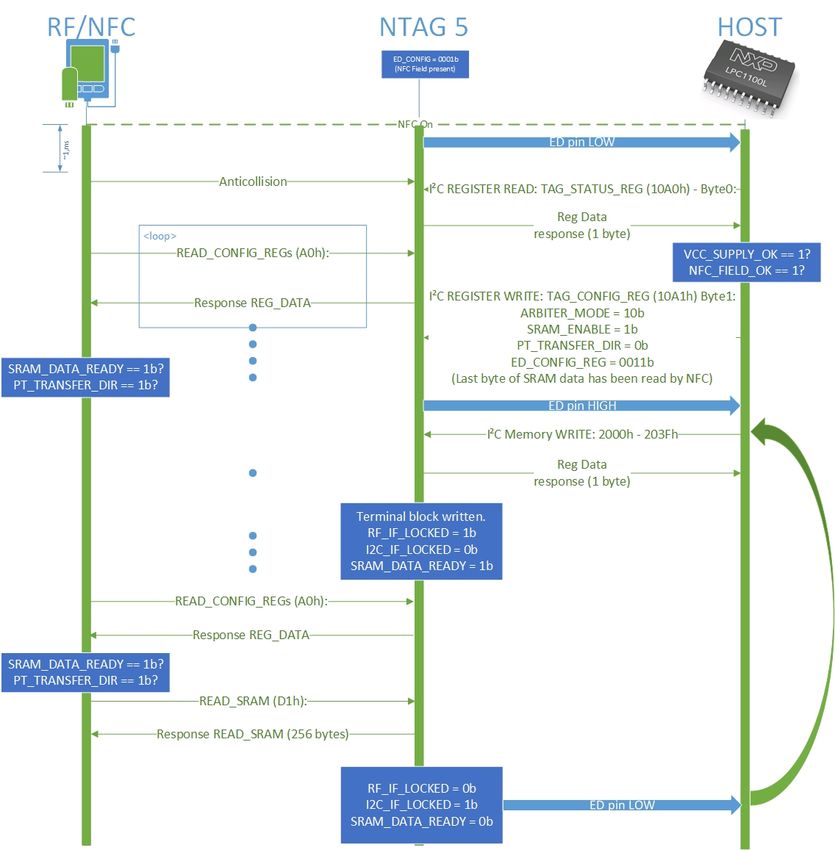
6.1 Data Transfer mechanism RF to I C Data transfer (RF reader to I C
host)
2
Figure 1. Passthrough procedure RF -> I C (example)
AN12364 All information provided in this document is subject to legal disclaimers. © NXP B.V. 2020. All rights reserved.
Application note Rev. 1.0 — 9 January 2020
COMPANY PUBLIC 530310 9 / 20NXP Semiconductors
AN12364
NTAG 5 - Bidirectional data exchange
Steps:
1. NTAG’s configuration (start-up behavior) is set that ED pin will go LOW once NFC
field is present
2. NFC field is present, 1 ms guard time (ISO15693) for NTAG to boot up
3. In the mean-time ED pin goes LOW
2
4. µC queries (sends I C commands in loop) for VCC and NFC field presence status
registers
5. If both 1b, move on
6. µC reset Session registers (current session):
• ARBITER_MODE: SRAM pass through
• Enable SRAM memory
• Pass-through direction: NFC->I2C
• ED goes LOW when last byte (Byte3 – block 3Fh) of SRAM is written
(ED_CONFIG_REG = 0100b)
7. Clear ED pin (ED pin is cleared i.e. released when writing 01h to the ED clear register
ED_INTR_ CLEAR_REG (10ACh))
8. NFC can start writing to SRAM
9. When the last page of SRAM is written, ED pin is pulled LOW
2
10.NFC polls if data was read from SRAM and/or arbiter still keeps access locked to I C
interface
2
11.I C side was notified through interrupt – ED pin, that data is waiting in SRAM. SRAM
Memory can be read now
2
12.ED pin goes low, when last byte has been READ by I C interface (ED_CONFIG_REG
= 0100b)
2
13.Arbiter unlocks access from I C interface and sets SRAM_DATA_READY bit to 0b.
NFC polls for those and can restart SRAM WRITE loop with new data.
AN12364 All information provided in this document is subject to legal disclaimers. © NXP B.V. 2020. All rights reserved.
Application note Rev. 1.0 — 9 January 2020
COMPANY PUBLIC 530310 10 / 20NXP Semiconductors
AN12364
NTAG 5 - Bidirectional data exchange
2 2
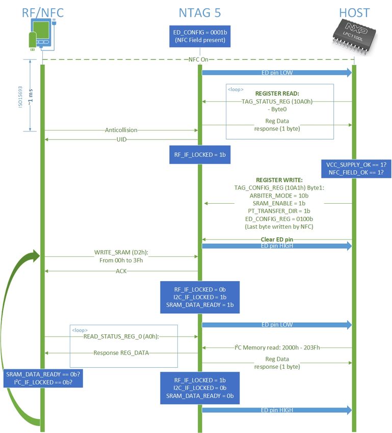
6.2 Data Transfer mechanism I C to RF Data transfer (I C host to RF
reader)
2
Figure 2. Passthrough procedure I C -> RF
AN12364 All information provided in this document is subject to legal disclaimers. © NXP B.V. 2020. All rights reserved.
Application note Rev. 1.0 — 9 January 2020
COMPANY PUBLIC 530310 11 / 20NXP Semiconductors
AN12364
NTAG 5 - Bidirectional data exchange
Steps:
1. NTAG’s configuration (start-up behavior) is set that ED pin will go LOW once NFC
field is present
2. NFC field is present, 1 ms guard time (ISO15693) for NTAG to boot up
3. In the mean-time ED pin goes LOW
4. RF polls when data is ready in SRAM (SRAM_DATA_READY)
2
5. I C host sets NTAG 5s session registers:
• arbiter mode: pass-through
• enable SRAM memory
2
• transfer direction: I C → RF
• configure ED pin to go low when last byte of SRAM page is read by NFC
2
6. I C host writes to SRAM memory (2000h - 203Fh)
2
7. When last byte of SRAM is written, Arbiter locks interface to RF and releases I C
interface. SRAM_DATA_READY bit is set to 1b on NTAG 5.
8. SRAM_DATA_READY is 1b, RF interface can read SRAM now
2
9. When last byte of SRAM is read by NFC, Arbiter locks to I C interface and
SRAM_DATA_READY bit is set back to 0b.
10.ED pin is pulled low
2
11.I C host can start to write another chunk of data or stop the pass-through.
AN12364 All information provided in this document is subject to legal disclaimers. © NXP B.V. 2020. All rights reserved.
Application note Rev. 1.0 — 9 January 2020
COMPANY PUBLIC 530310 12 / 20NXP Semiconductors
AN12364
NTAG 5 - Bidirectional data exchange
7 PHDC mode
This mode is defined by NFC Forum to be used in Personal Health Device
Communication. For more info, refer to [PHDC]. NFC Forum Reader/Writer Mode is
used.
ARBITER_MODE [1:0] = 11b indicates SRAM PHDC mode.
The arbitration scheme remains same as Normal mode with exception of SRAM access
for read.
To make this mode work, the tag needs to be powered by both RF & VCC.
• RF_FIELD_OK = 1b
• VCC_SUPPLY_OK = 1b
• SRAM_ENABLE = 1b
PHDC mode would map SRAM in user memory (EEPROM) space. SRAM is always
mirrored to block0h. In PHDC mode the SRAM is mirrored on to Block 0h of EEPROM
2
memory for both RF to I C interfaces.
In this mode the SRAM is mapped at memory:
2
• I C interface:
– Can be accessed at BLOCK0h to BLOCK3Fh or
– Can be accessed at 2000h-203Fh
• RF Interface:
– Can be accessed by read or write commands to SRAM mirrored blocks BLOCK0h to
BLOCK3Fh. NFC Forum commands which are used are specified in [PHDC]: NFC
read and NFC write
– Can be accessed by SRAM_READ and SRAM_WRITE Commands
SRAM access condition differs from Normal mode.
2
• I C Interface accessing SRAM
2
– I C_IF_LOCKED =1b
2
– I C SRAM read/write ongoing
– IF RF requests for SRAM access.
– RF read/write access:
2 2
- The current ongoing I C access is halted and I C clock is stretched after
2
completing the current Byte read or write access of I C interface.
2
I C_IF_LOCKED = 0 and NFC_IF_LOCKED =1
- RF gets the access to read/write SRAM.
2
- After RF reads/writes SRAM, I C transaction is resumed.
2
I C_IF_LOCKED = 1 and NFC_IF_LOCKED =0
AN12364 All information provided in this document is subject to legal disclaimers. © NXP B.V. 2020. All rights reserved.
Application note Rev. 1.0 — 9 January 2020
COMPANY PUBLIC 530310 13 / 20NXP Semiconductors
AN12364
NTAG 5 - Bidirectional data exchange
8 Configuration and SRAM memory password security
SRAM and EEPROM used for bidirectional data exchange can be optionally also
password protected. More details can be found in [Application note].
AN12364 All information provided in this document is subject to legal disclaimers. © NXP B.V. 2020. All rights reserved.
Application note Rev. 1.0 — 9 January 2020
COMPANY PUBLIC 530310 14 / 20NXP Semiconductors
AN12364
NTAG 5 - Bidirectional data exchange
9 References
[1] NFC Forum specification, Tag NDEF Exchange Protocol - Technical Specification
TM
Version 1.0 2019-04-24 [TNEP] NFC Forum
https://nfc-forum.org/our-work/specifications-and-application-documents/
specifications/nfc-forum-candidate-technical-specifications/
[2] NFC Forum Personal Health Care Devices (PHDC) specification
https://nfc-forum.org/product-category/specification/
[3] AN12366 - NTAG 5 Memory Configuration and Scalable Security, doc.no. 5305xx
https://www.nxp.com/docs/en/application-note/AN12366.pdf
[4] RM00221 - NTAG 5 Android Application development, doc.no. 5318xx
https://www.nxp.com/docs/en/reference-manual/RM00221.pdf
[5] RM00222 - NTAG 5 KW41 firmware development, doc.no. 5319xx
https://www.nxp.com/docs/en/reference-manual/RM00222.pdf
AN12364 All information provided in this document is subject to legal disclaimers. © NXP B.V. 2020. All rights reserved.
Application note Rev. 1.0 — 9 January 2020
COMPANY PUBLIC 530310 15 / 20NXP Semiconductors
AN12364
NTAG 5 - Bidirectional data exchange
10 Legal information
Export control — This document as well as the item(s) described herein
may be subject to export control regulations. Export might require a prior
10.1 Definitions authorization from competent authorities.
Draft — The document is a draft version only. The content is still under Non-automotive qualified products — Unless this data sheet expressly
internal review and subject to formal approval, which may result in states that this specific NXP Semiconductors product is automotive qualified,
modifications or additions. NXP Semiconductors does not give any the product is not suitable for automotive use. It is neither qualified nor
representations or warranties as to the accuracy or completeness of tested in accordance with automotive testing or application requirements.
information included herein and shall have no liability for the consequences NXP Semiconductors accepts no liability for inclusion and/or use of non-
of use of such information. automotive qualified products in automotive equipment or applications. In
the event that customer uses the product for design-in and use in automotive
applications to automotive specifications and standards, customer (a) shall
use the product without NXP Semiconductors’ warranty of the product for
10.2 Disclaimers such automotive applications, use and specifications, and (b) whenever
customer uses the product for automotive applications beyond NXP
Semiconductors’ specifications such use shall be solely at customer’s own
Limited warranty and liability — Information in this document is believed risk, and (c) customer fully indemnifies NXP Semiconductors for any liability,
to be accurate and reliable. However, NXP Semiconductors does not damages or failed product claims resulting from customer design and use
give any representations or warranties, expressed or implied, as to the of the product for automotive applications beyond NXP Semiconductors’
accuracy or completeness of such information and shall have no liability standard warranty and NXP Semiconductors’ product specifications.
for the consequences of use of such information. NXP Semiconductors
takes no responsibility for the content in this document if provided by an
Evaluation products — This product is provided on an “as is” and “with all
information source outside of NXP Semiconductors. In no event shall NXP
faults” basis for evaluation purposes only. NXP Semiconductors, its affiliates
Semiconductors be liable for any indirect, incidental, punitive, special or
and their suppliers expressly disclaim all warranties, whether express,
consequential damages (including - without limitation - lost profits, lost
implied or statutory, including but not limited to the implied warranties of
savings, business interruption, costs related to the removal or replacement
non-infringement, merchantability and fitness for a particular purpose. The
of any products or rework charges) whether or not such damages are based
entire risk as to the quality, or arising out of the use or performance, of this
on tort (including negligence), warranty, breach of contract or any other
product remains with customer. In no event shall NXP Semiconductors, its
legal theory. Notwithstanding any damages that customer might incur for
affiliates or their suppliers be liable to customer for any special, indirect,
any reason whatsoever, NXP Semiconductors’ aggregate and cumulative
consequential, punitive or incidental damages (including without limitation
liability towards customer for the products described herein shall be limited
damages for loss of business, business interruption, loss of use, loss of
in accordance with the Terms and conditions of commercial sale of NXP
data or information, and the like) arising out the use of or inability to use
Semiconductors.
the product, whether or not based on tort (including negligence), strict
liability, breach of contract, breach of warranty or any other theory, even if
Right to make changes — NXP Semiconductors reserves the right to advised of the possibility of such damages. Notwithstanding any damages
make changes to information published in this document, including without that customer might incur for any reason whatsoever (including without
limitation specifications and product descriptions, at any time and without limitation, all damages referenced above and all direct or general damages),
notice. This document supersedes and replaces all information supplied prior the entire liability of NXP Semiconductors, its affiliates and their suppliers
to the publication hereof. and customer’s exclusive remedy for all of the foregoing shall be limited to
actual damages incurred by customer based on reasonable reliance up to
Suitability for use — NXP Semiconductors products are not designed, the greater of the amount actually paid by customer for the product or five
authorized or warranted to be suitable for use in life support, life-critical or dollars (US$5.00). The foregoing limitations, exclusions and disclaimers
safety-critical systems or equipment, nor in applications where failure or shall apply to the maximum extent permitted by applicable law, even if any
malfunction of an NXP Semiconductors product can reasonably be expected remedy fails of its essential purpose.
to result in personal injury, death or severe property or environmental
damage. NXP Semiconductors and its suppliers accept no liability for Translations — A non-English (translated) version of a document is for
inclusion and/or use of NXP Semiconductors products in such equipment or reference only. The English version shall prevail in case of any discrepancy
applications and therefore such inclusion and/or use is at the customer’s own between the translated and English versions.
risk.
Security — While NXP Semiconductors has implemented advanced
Applications — Applications that are described herein for any of these security features, all products may be subject to unidentified vulnerabilities.
products are for illustrative purposes only. NXP Semiconductors makes Customers are responsible for the design and operation of their applications
no representation or warranty that such applications will be suitable and products to reduce the effect of these vulnerabilities on customer’s
for the specified use without further testing or modification. Customers applications and products, and NXP Semiconductors accepts no liability for
are responsible for the design and operation of their applications and any vulnerability that is discovered. Customers should implement appropriate
products using NXP Semiconductors products, and NXP Semiconductors design and operating safeguards to minimize the risks associated with their
accepts no liability for any assistance with applications or customer product applications and products.
design. It is customer’s sole responsibility to determine whether the NXP
Semiconductors product is suitable and fit for the customer’s applications
and products planned, as well as for the planned application and use of
customer’s third party customer(s). Customers should provide appropriate
design and operating safeguards to minimize the risks associated with 10.3 Licenses
their applications and products. NXP Semiconductors does not accept any
liability related to any default, damage, costs or problem which is based Purchase of NXP ICs with NFC technology
on any weakness or default in the customer’s applications or products, or
the application or use by customer’s third party customer(s). Customer is Purchase of an NXP Semiconductors IC that complies with one of the
responsible for doing all necessary testing for the customer’s applications Near Field Communication (NFC) standards ISO/IEC 18092 and ISO/
and products using NXP Semiconductors products in order to avoid a IEC 21481 does not convey an implied license under any patent right
default of the applications and the products or of the application or use by infringed by implementation of any of those standards. Purchase of NXP
customer’s third party customer(s). NXP does not accept any liability in this Semiconductors IC does not include a license to any NXP patent (or other
respect. IP right) covering combinations of those products with other products,
whether hardware or software.
AN12364 All information provided in this document is subject to legal disclaimers. © NXP B.V. 2020. All rights reserved.
Application note Rev. 1.0 — 9 January 2020
COMPANY PUBLIC 530310 16 / 20NXP Semiconductors
AN12364
NTAG 5 - Bidirectional data exchange
Notice: All referenced brands, product names, service names and
trademarks are the property of their respective owners.
10.4 Trademarks 2
I C-bus — logo is a trademark of NXP B.V.
NTAG — is a trademark of NXP B.V.
AN12364 All information provided in this document is subject to legal disclaimers. © NXP B.V. 2020. All rights reserved.
Application note Rev. 1.0 — 9 January 2020
COMPANY PUBLIC 530310 17 / 20NXP Semiconductors
AN12364
NTAG 5 - Bidirectional data exchange
Tables
Tab. 1. Abbreviations .....................................................3
AN12364 All information provided in this document is subject to legal disclaimers. © NXP B.V. 2020. All rights reserved.
Application note Rev. 1.0 — 9 January 2020
COMPANY PUBLIC 530310 18 / 20NXP Semiconductors
AN12364
NTAG 5 - Bidirectional data exchange
Figures
Fig. 1. Passthrough procedure RF -> I2C (example) .... 9 Fig. 2. Passthrough procedure I2C -> RF .................. 11
AN12364 All information provided in this document is subject to legal disclaimers. © NXP B.V. 2020. All rights reserved.
Application note Rev. 1.0 — 9 January 2020
COMPANY PUBLIC 530310 19 / 20NXP Semiconductors
AN12364
NTAG 5 - Bidirectional data exchange
Contents
1 Abbreviations ...................................................... 3
2 Introduction ......................................................... 4
2.1 Potential applications .........................................4
3 Interface Arbitration for memory access .......... 5
4 Normal Mode ....................................................... 6
5 SRAM Mirror Mode ............................................. 7
6 SRAM Pass-Through Mode ................................ 8
6.1 Data Transfer mechanism RF to I2C Data
transfer (RF reader to I2C host) ........................ 9
6.2 Data Transfer mechanism I2C to RF Data
transfer (I2C host to RF reader) ...................... 11
7 PHDC mode ....................................................... 13
8 Configuration and SRAM memory
password security .............................................14
9 References ......................................................... 15
10 Legal information .............................................. 16
Please be aware that important notices concerning this document and the product(s)
described herein, have been included in section 'Legal information'.
© NXP B.V. 2020. All rights reserved.
For more information, please visit: http://www.nxp.com
For sales office addresses, please send an email to: salesaddresses@nxp.com
Date of release: 9 January 2020
Document identifier: AN12364
Document number: 530310You can also read