IS37SML01G1 IS38SML01G1 - 1Gb SLC-1b ECC 3.3V SERIAL NAND FLASH MEMORY WITH 104MHZ MULTI I/O SPI INTERFACE DATA SHEET - Integrated Silicon ...
←
→
Page content transcription
If your browser does not render page correctly, please read the page content below
IS37SML01G1
IS38SML01G1
1Gb SLC-1b ECC
3.3V SERIAL NAND FLASH MEMORY WITH 104MHZ MULTI I/O SPI
INTERFACE

DATA SHEET
IS37/38SML01G1
1Gb 3.3V SPI-NAND FLASH MEMORY WITH 104MHZ MULTI I/O SPI
INTERFACE with 1b ECC
FEATURES
Flexible & Efficient Memory Efficient Read and Program modes
Architecture - Support SPI-Mode 0 and SPI-Mode 3
- Organization: - Bus Width: x1, x2(1), x4
- Memory Cell Array: (128M + 4M) x 8bit - Command Register Operation
- Data Register: (2K + 64) x 8bit - NOP: 4 cycles
- Page Size: (2K + 64) Byte - OTP Operation
- Block Erase: (128K + 4K) Byte - Bad-Block-Protect
- Memory Cell: 1bit/Memory Cell - Boot Read
Highest performance Advanced Security Protection
- Frequency : 104MHz - Hardware Data Protection
- Internal ECC Implementation: 1-bit ECC - Program/Erase Lockout during Power
- Read Performance Transitions
- Read from Cell to Register with Internal
ECC: 100us
Industry Standard Pin-out & Packages
- Write Performance - M =16-pin SOIC 300mil
- Program time: 400us - typical - L = 8-contact WSON 8x6mm
- Block Erase time: 4ms – typical
Low Power with Wide Temp. Ranges
- Single 3.3V (2.7V to 3.6V) Voltage
Supply
- 10 mA Active Read Current
- 8 µA Standby Current
- Temp Grades: Note:
- Industrial: -40°C to +85°C 1. X2 Program Operation is not defined.
- Extended: -40°C to +105°C
- Automotive, A1: -40°C to +85°C
- Automotive, A2: -40°C to +105°C
Reliable CMOS Floating Gate
Technology
- Internal ECC Requirement: 1bit/512Byte
- Endurance: 100K Program/Erase cycles
- Data Retention: 10 years
Integrated Silicon Solution, Inc.- www.issi.com 2
Rev. A2
09/13/2020
IS37/38SML01G1

GENERAL DESCRIPTION
The serial electrical interface follows the industry-standard serial peripheral interface (SPI), providing a
cost-effective non- volatile memory storage solution in systems where pin count must be kept to a
minimum.
The ISSI IS37/38SML01G1 is a 1Gb SLC SPI-NAND Flash memory device based on the standard
parallel NAND Flash, but new command protocols and registers are defined for SPI operation. It is also
an alternative to SPI-NOR, offering superior write performance and cost per bit over SPI-NOR.

The command set resembles common SPI-NOR command set, modified to handle NAND-specific
functions and new features. New features include user-selectable internal ECC. With internal ECC
enabled, ECC code is generated internally when a page is written to memory array. The ECC code is
stored in the spare area of each page. When a page is read to the cache register, the ECC code is
calculated again and compared with the stored value. Errors are corrected if necessary. The device
either outputs corrected data or returns an ECC error status.
The memory is divided into blocks that can be erased independently so it is possible to preserve valid
data while old data is erased. The device contains 1024 blocks, composed by 64 pages consisting in
two NAND structure of 32 series connected Flash cells. Each page consists 2112-Byte and is further
divided into a 2048-Byte data storage area with a separate 64-Byte spare area. The 64-Byte area is
typically used for memory and error management.
The copy back function allows the optimization of defective blocks management: when a page program
operation fails, the data can be directly programmed in another page inside the same array section
without the time consuming serial data insertion phase.
The pins serve as the ports for signals. The device has six signal lines plus Vcc and ground (GND, Vss).
The signal lines are SCK (serial clock), SI (command and data input), SO (response and data output),
and control signals CS#, HOLD#, WP#.

Integrated Silicon Solution, Inc.- www.issi.com                                             3
Rev. A2
09/13/2020
IS37/38SML01G1

TABLE OF CONTENTS

  FEATURES ............................................................................................................................................................ 2
  GENERAL DESCRIPTION .................................................................................................................................... 3
  TABLE OF CONTENTS ......................................................................................................................................... 4
  1.    PIN CONFIGURATION ................................................................................................................................... 6
  2.    PIN DESCRIPTIONS ...................................................................................................................................... 7
  3.    BLOCK DIAGRAM .......................................................................................................................................... 8
  4.    Command Set ................................................................................................................................................. 9
  5.    ELECTRICAL CHARACTERISTICS............................................................................................................. 10
        5.1 ABSOLUTE MAXIMUM RATINGS (1) ..................................................................................................... 10
        5.2 Recommended Operating Conditions .................................................................................................... 10
        5.3 DC CHARACTERISTICs ........................................................................................................................ 11
        5.4 Valid Block .............................................................................................................................................. 11
        5.5 AC Measurement Condition .................................................................................................................... 12
        5.6 AC PIN CAPACITANCE (TA = 25°C, VCC=3.3V, 1MHz) ...................................................................... 12
        5.7 READ/PROGRAM/ERASE PERFORMANCne ...................................................................................... 12
        5.8 General Timing Characteristics .............................................................................................................. 13
  6.    Operations and Timing Diagrams ................................................................................................................. 14
        6.1 Read Operations and Serial Output........................................................................................................ 14
        6.2 Program Operations and Serial Input ..................................................................................................... 20
        6.3 Internal Data Move.................................................................................................................................. 28
        6.4 Erase Operation ...................................................................................................................................... 28
        6.5 Read ID ................................................................................................................................................... 30
        6.6 WP# Timing ............................................................................................................................................ 31
        6.7 HOLD# Timing ........................................................................................................................................ 32
        6.8 Power-Up ................................................................................................................................................ 33
  7.    BUS/FEATURE OPERATION AND ERROR MANAGEMENT ..................................................................... 34
        7.1      BUS Operation ..................................................................................................................................... 34
        7.2      Feature Operations .............................................................................................................................. 35
        7.3      Array Write Enable / Disable ................................................................................................................ 37
        7.4      Status Register .................................................................................................................................... 38
        7.5      Error Management ............................................................................................................................... 39
        7.5.1 Mask Out Initial Invalid Blocks ............................................................................................................. 39
        7.5.2 Identifying Initial Invalid BlockS ........................................................................................................... 39
        7.5.3 Block Replacement .............................................................................................................................. 41
        7.5.4 ECC Protection .................................................................................................................................... 42
        7.6      Addressing for Programming Operation .............................................................................................. 43
  8.    PACKAGE TYPE INFORMATION ................................................................................................................ 44
        8.1      16-LEAD PLASTIC SMALL OUTLINE PACKAGE (300 MILS BODY WIDTH) (M) ............................. 44

Integrated Silicon Solution, Inc.- www.issi.com                                                                                                 4
Rev. A2
09/13/2020
IS37/38SML01G1
8.2 8-CONTACT ULTRA-THIN SMALL OUTLINE NO-LEAD (WSON) PACKAGE 8x6mm (L)................ 45
9. ORDERING INFORMATION – Valid Part Numbers ..................................................................................... 46
Integrated Silicon Solution, Inc.- www.issi.com 5
Rev. A2
09/13/2020IS37/38SML01G1
1. PIN CONFIGURATION
HOLD# (IO3) 1 16 SCK
Vcc 2 15 SI (IO0)
NC 3 14 NC
CS# 1 8 Vcc
NC 4 13 NC
HOLD# (IO3)
SO (IO1) 2 7 (1)
NC 5 12 NC
NC 6 11 NC WP# (IO2) 3 6 SCK
CS# 7 10 Vss
Vss 4 5 SI (IO0)
SO (IO1) 8 9 WP# (IO2)
16-pin SOIC 300mil 8-contact WSON 8x6mm
Integrated Silicon Solution, Inc.- www.issi.com 6
Rev. A2
09/13/2020IS37/38SML01G1
2. PIN DESCRIPTIONS
SYMBOL TYPE DESCRIPTION
Chip Select:
(1)
The device is activated/deactivated as CS# is driven LOW /HIGH (2).
CS# INPUT After power-on, the device requires a falling edge on CS# before any command can
be written. The device goes to standby mode when no PROGRAM, ERASE, or
WRITE STATUS REGISTER operation is in progress.
HOLD#/IO3:
Hold pauses any serial communication with the device without deselecting it. (3) When
INPUT/ driven LOW, SO is at high impedance (Hi-Z), and all inputs in SI and SCK are ignored;
HOLD# / IO3
OUTPUT CS# also should be driven LOW.
HOLD# must not be driven during x4 operation.
Write Protect#/IO2:
INPUT/ WP# is driven LOW to prevent overwriting the block-lock bits (BP0,BP1 and BP2). If
WP# / IO2 block register write disable (BRWD) bit is set. (4)
OUTPUT
WP# must not be driven during x4 operation.
Serial Clock:
SCK provides serial interfacing timing.
SCK INPUT Address, commands, and data in SI are latched on the rising edge of SCK.
Output (data out SO) is triggered after the falling edge of SCK.
The clock is valid only when the device is active. (5)
Serial Data Input/IO0:
SI transfers data serially into the device. Device latches addresses, commands, and
SI / IO0 INPUT/OUTPUT program data in SI on the rising-edge of SCK.
SI must not be driven during x2 or x4 READ operation.
Serial Data Output/IO1:
SO / IO1 INPUT/OUTPUT SO transfers data serially out of the device on the falling edge of SCK.. K.
SO must not be driven during x2 or x4 PROGRAM operation.
Vcc(6) POWER Vcc is the power supply for device.
Vss(6) GROUND Ground
No Connection
NC Unused
Not internally connected.
Notes:
1. CS# places the device in active power mode.
2. CS# deselects the device and places SO at high impedance.
3. It means HOLD# input doesn’t terminate any READ, PROGRAM, or ERASE operation currently in progress.
4. If the BRWD bit is set to 1 and WP# is LOW, the block protect bits can’t be altered.
5. SI and SO can be triggered only when the clock is valid.
6. Connect all Vcc and Vss pins of each device to common power supply outputs. Do not leave Vcc or Vss
disconnected.
Integrated Silicon Solution, Inc.- www.issi.com 7
Rev. A2
09/13/2020IS37/38SML01G1 3. BLOCK DIAGRAM Figure 3.1 Functional Block Diagram Figure 3.2 Array Organization Integrated Silicon Solution, Inc.- www.issi.com 8 Rev. A2 09/13/2020
IS37/38SML01G1

4. Command Set
Table 4.1 Command Set

                Command                  Op Code     Address Bytes      Dummy Bytes                Data Bytes

Block Erase                                 D8h             3                  0                        0
Get   Feature(1)                            0Fh             1                  0                        1
Set Feature                                 1Fh             1                  0                        1
Write Disable                               04h             0                  0                        0
Write Enable                                06h             0                  0                        0
Program Load                                02h             2                  0                   1 to 2112
Program Load       x4(2)                    32h             2                  0                   1 to 2112
Program Load Random Data                    84h             2                  0                   1 to 2112
Program Load Random Data       x4(2)        34h             2                  0                   1 to 2112
Program Execute                             10h             3                  0                        0
Page Read                                   13h             3                  0                        0
Read from Cache                          03h, 0Bh           2                  1                   1 to 2112
Read from Cache x2                          3Bh             2                  1                   1 to 2112
Read from Cache x4(2)                       6Bh             2                  1                   1 to 2112
Read ID                                     9Fh             0                  1                        5
RESET                                       FFh             0                  0                        0

Notes:
1. Refer to Feature Register.
2. Command/Address is 1-bit input per clock period, data is 4-bit input/output per clock period.

Integrated Silicon Solution, Inc.- www.issi.com                                                     9
Rev. A2
09/13/2020
IS37/38SML01G1
5. ELECTRICAL CHARACTERISTICS
5.1 ABSOLUTE MAXIMUM RATINGS (1)
Storage Temperature -65°C to +150°C
Standard Package 240°C 3 Seconds
Surface Mount Lead Soldering Temperature
Lead-free Package 260°C 3 Seconds
Input Voltage with Respect to Ground on All Pins -0.6V to +4.6V
All I/O Voltage with Respect to Ground -0.6V to VCC + 0.3V( < 4.6V)
VCC -0.6V to +4.6V
Short Circuit Current 5mA
Electrostatic Discharge Voltage (Human Body Model)(2) -2000V to +2000V
Notes:
1. Applied conditions greater than those listed in “Absolute Maximum Ratings” may cause permanent damage to the
device. This is a stress rating only and functional operation of the device at these or any other conditions above
those indicated in the operational sections of this specification is not implied. Exposure to absolute maximum
rating conditions for extended periods may affect reliability.
2. ANSI/ESDA/JEDEC JS-001
5.2 RECOMMENDED OPERATING CONDITIONS
Part Number IS37/38SML01G1
Operating Temperature (Industrial Grade) -40°C to 85°C
Operating Temperature (Extended Grade) -40°C to 105°C
Operating Temperature (Automotive Grade A1) -40°C to 85°C
Operating Temperature (Automotive Grade A2) -40°C to 105°C
VCC Power Supply 2.7V (VMIN) – 3.6V (VMAX); 3.3V (Typ)
Integrated Silicon Solution, Inc.- www.issi.com 10
Rev. A2
09/13/2020IS37/38SML01G1
5.3 DC CHARACTERISTICS
(Under operating range)
Parameter Symbol Test Conditions Min Typ. Max Unit
Page Read fC=104MHz,
ICC1 - 16
with Serial Access CS#=VIL, IOUT=0mA
Operating
Current Program ICC2 - - 16 20 mA
Erase ICC3 - - 16
Stand-by Current (TTL) ISB1 CS#=VIH, WP#=0V/Vcc - - 1
CS#=VCC-0.2,
Stand-by Current (CMOS) ISB2 - 10 50
WP#=0V/Vcc
Input Leakage Current ILI VIN=0 to Vcc (max) - - +/-10 uA
Output Leakage Current ILO VOUT=0 to Vcc (max) - - +/-10
Input High Voltage VIH (1) 0.7xVCC - Vcc+0.3
Input Low Voltage, All inputs VIL (1) -0.3 - 0.2xVCC V
Output High Voltage Level VOH IOH=-20 uA 0.7xVCC - -
Output Low Voltage Level VOL IOL=1mA - - 0.15xVCC
Notes:
1. VIL can undershoot to - 2V and VIH can overshoot to Vcc + 2V for durations of 20 ns or less.
2. Typical value are measured at Vcc=3.3V, TA=25℃. Not 100% tested.
5.4 VALID BLOCK
Description Requirement
Minimum / Maximum number of Valid block number 1004 / 1024
Bad Block Mark Non FFh
Mark Location Column 2048 of page 0 and page 1
Notes:
1. The device may include initial invalid blocks when first shipped. Additional invalid blocks may develop while being used. The number
of valid blocks is presented with both cases of invalid blocks considered. Invalid blocks are defined as blocks that contain one or more
bad bits which cause status failure during program and erase operation. Do not erase or program factory-marked bad blocks.
2. The 1st block, which is placed on 00h block address, is guaranteed to be a valid block at the time of shipment and is guaranteed to
be a valid block up to 1K program/erase cycles with 1bit/512Byte ECC.
Integrated Silicon Solution, Inc.- www.issi.com 11
Rev. A2
09/13/2020IS37/38SML01G1
5.5 AC MEASUREMENT CONDITION
Symbol Parameter Min Max Units
CL Output Load 1 TTL GATE and CL = 15pF pF
TR,TF Input Rise and Fall Times - 2.4 ns
VIN Input Pulse Voltages 0.2Vcc to 0.8 VCC V
5.6 AC PIN CAPACITANCE (TA = 25°C, VCC=3.3V, 1MHZ)
Symbol Parameter Test Condition Min Typ Max Units
CIN Input Capacitance VIN = 0V - - 8 pF
CI/O Input /Output Capacitance VI/O = 0V - - 8 pF
Note:
1. These parameters are characterized and not 100% tested.
5.7 READ/PROGRAM/ERASE PERFORMANCNE
(Industrial: TA=-40 to 85℃, Automotive, A1: TA=-40 to 85℃, Vcc=2.7V ~ 3.6V)
Parameter Symbol Min Typ Max Unit
Average Program Time tPROG - 400 900 us
Number of Partial Program Cycles in the Same Page NOP - - 4 cycle
Block Erase Time tBERS - 4 10 ms
Data Transfer from Cell to Register with Internal ECC tRD - - 100 us
Integrated Silicon Solution, Inc.- www.issi.com 12
Rev. A2
09/13/2020IS37/38SML01G1 5.8 GENERAL TIMING CHARACTERISTICS Note: 1. For the first RESET condition after power up, tRST will be 1ms MAX. Integrated Silicon Solution, Inc.- www.issi.com 13 Rev. A2 09/13/2020
IS37/38SML01G1
6. Operations and Timing Diagrams
6.1 READ OPERATIONS AND SERIAL OUTPUT
The command sequence is as follows:
13h (PAGE READ to cache)
0Fh (GET FEATURE command to read the status)
0Bh or 03h (READ FROM CACHE x1)/ 3Bh (x2) / 6Bh (x4)
PAGE READ command requires 24-bit address with 8 dummy and a 16-bit row address. After row
address is registered, the device starts the transfer from the main array to the cache register, and is busy
for tRD time. During this time, GET FEATURE command can be issued to monitor the status of the
operation. Following a status of successful completion, READ FROM CACHE command must be issued
to read the data out of the cache.
READ FROM CACHE command requires 16-bit address with 4 dummy bits and 12-bit column address
for the starting byte. The starting byte can be 0 to 2111, but after the end of the cache register is reached,
the data does not wrap around and SO goes to a Hi-Z state.
Integrated Silicon Solution, Inc.- www.issi.com 14
Rev. A2
09/13/2020IS37/38SML01G1
Figure 6.1 PAGE READ (13h) Timing
Integrated Silicon Solution, Inc.- www.issi.com 15
Rev. A2
09/13/2020IS37/38SML01G1 Figure 6.2 READ FROM CACHE (03h or 0Bh) Timing Integrated Silicon Solution, Inc.- www.issi.com 16 Rev. A2 09/13/2020
IS37/38SML01G1

Figure 6.3 READ FROM CACHE x2 (3Bh) Timing

Integrated Silicon Solution, Inc.- www.issi.com        17
Rev. A2
09/13/2020
IS37/38SML01G1

    Figure 6.4 READ FROM CACHE x4 (6Bh) Timing

Integrated Silicon Solution, Inc.- www.issi.com        18
Rev. A2
09/13/2020
IS37/38SML01G1 Figure 6.5 SERIAL OUTPUT Timing Integrated Silicon Solution, Inc.- www.issi.com 19 Rev. A2 09/13/2020
IS37/38SML01G1
6.2 PROGRAM OPERATIONS AND SERIAL INPUT
6.2.1 Page Program
The command sequence is as follows:
06h (WRITE ENABLE)
02h (PROGRAM LOAD x1) / 32h (x4)
10h (PROGRAM EXECUTE)
0Fh (GET FEATURE command to read the status)
The page program operation sequence programs 1 byte to 2112 bytes of data within a page. WRITE
ENABLE command is not issued (WEL bit is not set), then the rest of the program sequence is ignored.
PROGRAM LOAD command requires 16-bit address with 4 dummy and a 12-bit column address, then
the data bytes to be loaded into cache register. Only four partial page programs are allowed on a single
page. If more than 2112 bytes are loaded, then those additional bytes are ignored by the cache register.
After the data is loaded, PROGRAM EXECUTE command must be issued to transfer the data from
cache register to main array, and is busy for tPROG time. PROGRAM EXECUTE command requires 24-
bit address with 8 dummy bits and a 16-bit row address.
Figure 6.6 PROGRAM LOAD (02h) Timing
Integrated Silicon Solution, Inc.- www.issi.com 20
Rev. A2
09/13/2020IS37/38SML01G1 Figure 6.7 PROGRAM LOAD x4 (32h) Timing Integrated Silicon Solution, Inc.- www.issi.com 21 Rev. A2 09/13/2020
IS37/38SML01G1

Integrated Silicon Solution, Inc.- www.issi.com        22
Rev. A2
09/13/2020
IS37/38SML01G1

Integrated Silicon Solution, Inc.- www.issi.com        23
Rev. A2
09/13/2020
IS37/38SML01G1
Figure 6.8 PROGRAM EXECUTE (10h) Timing
6.2.2 Random Data Program
The command sequence is as follows:
06h (WRITE ENABLE)
84h (PROGRAM LOAD RANDOM DATA x1) / 34h (x4)
10h (PROGRAM EXECUTE)
0Fh (GET FEATURE command to read the status)
The random data program operation sequence programs or replaces data in a page with existing data.
PROGRAM LOAD RANDOM DATA command requires 16-bit address with 4 dummy bits and a 12-bit
column address. New data is loaded in the column address provided. If the random data is not sequential,
then another PROGRAM LOAD RANDOM DATA command must be issued with a new column address.
After the data is loaded, PROGRAM EXECUTE command can be issued to start the programming
operation.
Integrated Silicon Solution, Inc.- www.issi.com 24
Rev. A2
09/13/2020IS37/38SML01G1 Figure 6.9 PROGRAM LOAD RANDOM DATA (84h) Timing Integrated Silicon Solution, Inc.- www.issi.com 25 Rev. A2 09/13/2020
IS37/38SML01G1

Figure 6.10 PROGRAM LOAD RANDOM DATA x4 (34h) Timing

Integrated Silicon Solution, Inc.- www.issi.com             26
Rev. A2
09/13/2020
IS37/38SML01G1

Figure 6.11 Serial Input and tCSCL Timing

Integrated Silicon Solution, Inc.- www.issi.com        27
Rev. A2
09/13/2020
IS37/38SML01G1
6.3 INTERNAL DATA MOVE
The command sequence is as follows:
13h (PAGE READ to cache)
06h (WRITE ENABLE)
84h (PROGRAM LOAD RANDOM DATA x1) / 34h(x4); this is OPTIONAL in sequence
10h (PROGRAM EXECUTE)
0Fh (GET FEATURE command to read the status)
The INTERNAL DATA MOVE operation sequence programs or replaces data in a page with existing
data. Prior to performing an INTERNAL DATA MOVE operation, the target page content must be read
into the cache register. PAGE READ command must be followed with a WRITE ENABLE command to
change the contents of memory array.
6.4 ERASE OPERATION
The command sequence is as follows:
06h (WRITE ENABLE)
D8h (BLOCK ERASE)
0Fh (GET FEATURE command to read the status)
BLOCK ERASE command requires 24-bit address with 8 dummy bits and a 16-bit row address. If
WRITE ENABLE command is not issued (WEL bit is not set), then the rest of the erase sequence is
ignored. After the row address is registered, the control logic automatically controls the timing and the
erase-verify operations, and the device is busy for tBERS time. BLOCK ERASE command operates on one
block at a time.
Integrated Silicon Solution, Inc.- www.issi.com 28
Rev. A2
09/13/2020IS37/38SML01G1 Figure 6.12 BLOCK ERASE (D8h) Timing Integrated Silicon Solution, Inc.- www.issi.com 29 Rev. A2 09/13/2020
IS37/38SML01G1

6.5 READ ID

  The device contains a product identification mode, initiated by writing 9Fh to the command register.
Five read cycles sequentially output the manufacturer code (C8h) and the device code and 3 rd, 4th, 5th
cycle ID respectively after a dummy byte. The command register remains in Read ID mode until further
commands are issued to it.

Figure 6.13 Read ID Timing

                             1st Cycle        2nd Cycle
        Part No.                                            3rd Cycle   4th Cycle       5th Cycle
                           (Maker Code)     (Device Code)
   IS37/38SML01G1               C8h               21h         7Fh          7Fh             7Fh

Integrated Silicon Solution, Inc.- www.issi.com                                       30
Rev. A2
09/13/2020
IS37/38SML01G1 Table 6.1 ID Definition Table 6.6 WP# TIMING Figure 6.14 WP# Timing Integrated Silicon Solution, Inc.- www.issi.com 31 Rev. A2 09/13/2020
IS37/38SML01G1

6.7 HOLD# TIMING

 HOLD# input provides a method to pause serial communication with the device but doesn’t terminate
any READ, PROGRAM, or ERASE operation currently in progress.
   Hold mode starts at the falling edge of HOLD# provided SCK is also Low. If SCK is High when HOLD#
goes Low, hold mode begins after the next falling edge of SCK. Similarly, hold mode is exited at the
rising edge of HOLD# provided SCK is also Low. If SCK is High, hold mode ends after the next falling
edge of SCK.
  During hold mode, SO is Hi-Z, and SCK inputs are ignored.

Figure 6.15 HOLD# Timing

Integrated Silicon Solution, Inc.- www.issi.com                                    32
Rev. A2
09/13/2020
IS37/38SML01G1

6.8 POWER-UP

During power transitions, the device can be selected after tVCE. CS# = HIGH is recommended until the end of
tVCE.

                    VCC

   VCC ( max)

                                       Chip Selection Not Allowed

   VCC(min)

                                                               tVCE          Device is fully
                                                                               accessible
                                                     = Vcc min. to CE# Low

        VWI

                                                                                                             Time

Figure 6.16 Power-Up Timing

     Symbol                                       Parameter                           Min.       Max                Unit
      tVCE(1)             Vcc(min) to CE# Low                                        1250                           us
              (1)
        VWI               Write Inhibit Voltage                                                   2.5                V

Note: 1.These parameters are characterized and not 100% tested.
Table 6.2 Power Up Timing Table

Integrated Silicon Solution, Inc.- www.issi.com                                                         33
Rev. A2
09/13/2020
IS37/38SML01G1 Table 6.1 ID Definition Table 7. BUS/FEATURE OPERATION AND ERROR MANAGEMENT 7.1 BUS OPERATION SPI NAND supports two SPI modes: (Mode 0) CPOL (clock polarity) = 0, CPHA (clock phase) = 0 (Mode 1) CPOL (clock polarity) = 1, CPHA (clock phase) = 1 Input data is latched in on the rising edge of SCK, and output data is available from the falling edge of SCK for both modes. When CS# is High, keep SCK at Vss (Mode 0) or Vcc (Mode 3). Do not begin toggling SCK until after CS# is driven Low. Figure 7.1 SPI Modes Timing Integrated Silicon Solution, Inc.- www.issi.com 34 Rev. A2 09/13/2020
IS37/38SML01G1

7.2 FEATURE OPERATIONS
The GET FEATURE (0Fh) and SET FEATURE (1Fh) commands are used to alter the device behavior
from the default power-on behavior. These commands use a 1-Byte feature address to determine which
feature is to be read or modified.
When a feature is set, it remains active until the device is power cycled or the feature is written to.
Unless otherwise specified in the below Table, once the device is set, it remains set, even if a RESET
(FFh) command is issued.

                 Table 7.1 Feature Settings

Notes:
     1. 38h is the default data byte value for Block Lock Register after power-up.
     2. 1-bit internal ECC for all READ and PROGRAM operations can be enabled (ECC enable = 1) or
        disabled (ECC disable = 0); (10h) is the default data byte value for OTP Register after power-up.
     3. WEL = 0 is the default data bit value for Status Register after power-up.
     4. (20h) is the default data byte value for Output Driver Register after power-up
                   Table 7.2 Block Protect Bits of Block Lock Register

Integrated Silicon Solution, Inc.- www.issi.com                                            35
Rev. A2
09/13/2020
IS37/38SML01G1
Table 7.3 OTP Status Bits of OTP Register
Table 7.4 Driver Strength Bits of Output Driver Register
Figure 7.2 GET FEATURE (0Fh) Timing
Figure 7.2 SET FEATURE (1Fh) Timing
Integrated Silicon Solution, Inc.- www.issi.com 36
Rev. A2
09/13/2020IS37/38SML01G1 7.3 ARRAY WRITE ENABLE / DISABLE The WRITE ENABLE (06h) command sets the WEL bit (in status register) to 1. This required in the following WRITE operations that change the contents of the memory array. PAGE PROGRAM, BLOCK ERASE, and OTP PROGRAM. Contrarily, the WRITE DISABLE (04h) command sets the WEL bit to 0. This disables PAGE PROGRAM, BLOCK ERASE, and OTP PROGRAM. Figure 7.3 WRITE ENABLE (06h) Timing Figure 7.4 WRITE DISABLE (04h) Timing Integrated Silicon Solution, Inc.- www.issi.com 37 Rev. A2 09/13/2020
IS37/38SML01G1

7.4 STATUS REGISTER
Software can read status register during the NAND device operation by issuing GET FEATURE (0Fh)
command, followed by the feature address C0h. The status register will output the status of the operation.
Refer to Table 7.1, Table 7.5 and Table 7.6.

                   Table 7.5 Bits of Status Register
      Bit           Name            Mode                                     DESCRIPTION
                                                  ECC_S1 and ECC_S0 are set to 00h either following a RESET, or at
                                                  the beginning of the READ. Then updated after the device completes a
                ECC_S1,                           valid READ operation.
     [5:4]                             R
                ECC_S0
                                                  ECC_S1/S0 are invalid if ECC is disabled. After power-up, ECC_S1
                                                  and ECC_S2 are set to reflect the contents of block 0, page 0.
                                                  P_Fail is set to “1” as a program failure has occurred. P_Fail = “1” will
                                                  also be set if the user attempts to program an invalid address or a
        [3]     Program Fail           R          locked region.
                                                  P_Fail is set to “0” during the PROGRAM EXECUTE command
                                                  sequence or the RESET command.
                                                  E_Fail is set to “1” as an erase failure has occurred. E_Fail = “1” will
                                                  also be set if the user attempts to erase a locked region, or if ERASE
        [2]     Erase Fail             R          operation fails.
                                                  E_Fail is set to “0” during the BLOCK ERASE command sequence or
                                                  the RESET command.
                                                  WEL must be set to ‘1” to indicate the current status of the write enable
                Write Enable                      latch, prior to issuing PROGRAM EXECUTE or BLOCK ERASE
        [1]                           W           command. It is set by issuing WRITE ENABLE command. WEL is
                Latch
                                                  disabled (WEL=”0”) by issuing the WRITE DISABLE command.
                                                  OIP is set to “1” when the device is busy; it means a PROGRAM
                Operation In                      EXECUTE, PAGE READ, BLOCK ERASE, or RESET command is
        [0]                            R
                Progress                          executing. OIP is cleared to “0” as the interface is in ready state.

                   Table 7.6 ECC Status Bits of Status Register

Integrated Silicon Solution, Inc.- www.issi.com                                                         38
Rev. A2
09/13/2020
IS37/38SML01G1 7.5 ERROR MANAGEMENT 7.5.1 MASK OUT INITIAL INVALID BLOCKS Initial invalid blocks are defined as blocks that contain one or more initial invalid bits whose reliability is not guaranteed by ISSI. The information regarding the initial invalid blocks is called the initial invalid block information. Devices with initial invalid block(s) have the same quality level as devices with all valid blocks and have the same AC and DC characteristics. An initial invalid block(s) does not affect the performance of valid block(s) because it is isolated from the bit line and the common source line by a select transistor. The system design must be able to mask out the initial invalid block(s) via address mapping. The 1st block, which is placed on 00h block address, is guaranteed to be a valid block up to 1K program/erase cycles with 1bit/512Byte ECC. 7.5.2 IDENTIFYING INITIAL INVALID BLOCKS Unpredictable behavior may result from programming or erasing the defective blocks. Figure 7.5 below illustrates an algorithm for searching factory-mapped defects, and the algorithm needs to be executed prior to any erase or program operations. A host controller has to scan blocks from block 0 to the last block using page read command and check the data at the column address of 2,048 of page 0 and page 1. If the read data is not FFh, the block is interpreted as an invalid block. Do not erase or program factory-marked bad blocks. The host controller must be able to recognize the initial invalid block information and to create a corresponding table to manage block replacement upon erase or program error when additional invalid blocks develop with Flash memory usage. Integrated Silicon Solution, Inc.- www.issi.com 39 Rev. A2 09/13/2020
IS37/38SML01G1

                                                                            Check “FFh” at column address 2048
                                                                            of the first page and the second page

   For (i=0; i
IS37/38SML01G1 7.5.3 BLOCK REPLACEMENT Within its lifetime, number of invalid blocks may increase with NAND Flash memory. Refer to the qualification report for the actual data. The following possible failure modes should be considered to implement a highly reliable system. In the case of failure after ERASE or PROGRAM in status register, block replacement should be done. Because PROGRAM status fail during a page program does not affect the data of other pages in the same block, block replacement can be executed with a page-sized buffer by finding an erased empty block and reprogramming the current target data and copying the rest of the replaced block. In case of READ, ECC must be employed. To improve the efficiency of memory space, it is recommended that read or verification failure due to single bit error be reclaimed by ECC without any block replacement. The additional block failure rate does not include those reclaimed blocks. Figure 7.6 Blcok Replacement Integrated Silicon Solution, Inc.- www.issi.com 41 Rev. A2 09/13/2020
IS37/38SML01G1

7.5.4 ECC PROTECTION
ECC is enabled after device power-up, so the default PROGRAM and READ commands operate with
internal ECC in the active state.

During a PROGRAM operation, the device calculates an ECC code on the 2KB page in the cache
register, before the page is written to the NAND Flash array. The ECC code is stored in the spare area
of the page in array.

During a READ operation, the page data is read from the array to the cache register, where ECC code
is calculated and compared with the ECC code value read from the array. If a single-bit data error is
discovered, the error is corrected in the cache register and only the corrected data is on the output pins.
                   Table 7.7 ECC Protection

Notes:
     1. The user area must be programmed within a single partial-page programming operations so NAND
        Flash device can calculate the proper ECC bytes.
     2. When internal ECC is enabled, these areas are prohibited to be programming.

Integrated Silicon Solution, Inc.- www.issi.com                                          42
Rev. A2
09/13/2020
IS37/38SML01G1 7.6 ADDRESSING FOR PROGRAMMING OPERATION Within a block, the page must be programmed consecutively from the LSB (Least Significant Bit) page of the block to MSB (Most Significant Bit) pages of the block. Random page address programming is prohibited. In this case, the definition of LSB page is the LSB among the pages to be programmed. Therefore, LSB page doesn’t need to be page 0. Figure 7.7 Addressing for Program Operation Integrated Silicon Solution, Inc.- www.issi.com 43 Rev. A2 09/13/2020
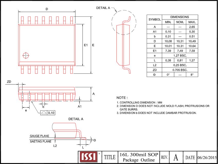
IS37/38SML01G1

8. PACKAGE TYPE INFORMATION
8.1 16-LEAD PLASTIC SMALL OUTLINE PACKAGE (300 MILS BODY WIDTH) (M)

Integrated Silicon Solution, Inc.- www.issi.com                        44
Rev. A2
09/13/2020
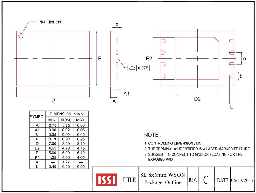
IS37/38SML01G1

8.2 8-CONTACT ULTRA-THIN SMALL OUTLINE NO-LEAD (WSON) PACKAGE 8X6MM (L)

Integrated Silicon Solution, Inc.- www.issi.com                           45
Rev. A2
09/13/2020
IS37/38SML01G1

9. ORDERING INFORMATION – Valid Part Numbers
    IS 37 SM L 01G 1            - M L I

                                                          TEMPERATURE RANGE
                                                          I = Industrial (-40°C to +85°C)
                                                          E = Industrial (-40°C to +105°C)
                                                          A1 = Automotive Grade (-40°C to +85°C)
                                                          A2 = Automotive Grade (-40°C to +105°C)

                                                          PACKAGING CONTENT
                                                          L = RoHS compliant

                                                          PACKAGE Type
                                                          L = 8-contact WSON (8x6mm)
                                                          M = 16-pin SOIC 300mil

                                                          Die Revision
                                                          Blank = First Gen.

                                                          ECC Requirement
                                                          1 = 1-bit ECC

                                                          Density
                                                          01G = 1 Gigabit

                                                          VDD
                                                          L = 3.3V

                                                          Technology
                                                          SM = SPI-NAND (SLC)

                                                          Product Family
                                                          37 = SPI-NAND
                                                          38 = Automotive SPI-NAND

                                                          BASE PART NUMBER
                                                          IS = Integrated Silicon Solution Inc.
        Note:
        1. Call Factory for other package options available.

Integrated Silicon Solution, Inc.- www.issi.com                                                     46
Rev. A2
09/13/2020
IS37/38SML01G1
VDD Density Bus Temp. Grade Order Part Number Package
IS37SML01G1-MLI 16-pin SOIC 300mil
Industrial
IS37SML01G1-LLI 8-contact WSON 8x6mm
IS38SML01G1-MLA1 16-pin SOIC 300mil
Automotive (A1)
IS38SML01G1-LLA1 8-contact WSON 8x6mm
3.3V 1Gb X8
IS37SML01G1-MLE 16-pin SOIC 300mil
Extended
IS37SML01G1-LLE 8-contact WSON 8x6mm
IS38SML01G1-MLA2 16-pin SOIC 300mil
Automotive (A2)
IS38SML01G1-LLA2 8-contact WSON 8x6mm
Integrated Silicon Solution, Inc.- www.issi.com 47
Rev. A2
09/13/2020You can also read