UM10412 UBA2021 evaluation board Rev. 1 - 2 November 2010 - User manual - NXP Semiconductors

Page created by Ernest Carlson
 
CONTINUE READING
UM10412 UBA2021 evaluation board Rev. 1 - 2 November 2010 - User manual - NXP Semiconductors
UM10412
  UBA2021 evaluation board
  Rev. 1 — 2 November 2010                                                    User manual

Document information
Info                   Content
Keywords               UBA2021, evaluation board, TL, CFL
Abstract               This document is the user manual for the UBA2021 evaluation board.
UM10412 UBA2021 evaluation board Rev. 1 - 2 November 2010 - User manual - NXP Semiconductors
NXP Semiconductors                                                                                                           UM10412
                                                                                                                      UBA2021 evaluation board

Revision history
Rev           Date         Description
01            20101102     First issue

Contact information
For more information, please visit: http://www.nxp.com
For sales office addresses, please send an email to: salesaddresses@nxp.com
UM10412                                  All information provided in this document is subject to legal disclaimers.           © NXP B.V. 2010. All rights reserved.

User manual                                           Rev. 1 — 2 November 2010                                                                         2 of 26
NXP Semiconductors                                                                                                                     UM10412
                                                                                                                             UBA2021 evaluation board

1. Introduction
                       This document describes the UBA2021 main board in combination with the UBA2021
                       daughter board. The main board is designed to be a flexible platform for demonstrating
                       the functionality of the UBA2014 and UBA2021 fluorescent tube drivers in different
                       applications. Please note that this board is not a complete ballast design for fluorescent
                       tubes. The default setup permits a T5 HE 35 W fluorescent lamp to be demonstrated.

2. Safety warnings and cautions

WARNING
Lethal voltage and fire ignition hazard
                             The non-insulated high voltages that are present when operating this product, constitute a
                             risk of electric shock, personal injury, death and/or ignition of fire.
                             This product is intended for evaluation purposes only. It shall be operated in a designated test
                             area by personnel qualified according to local requirements and labor laws to work with
                             non-insulated mains voltages and high-voltage circuits. This product shall never be operated
                             unattended.

                       Remark: Galvanic isolation of the mains phase using a variable transformer is always
                       recommended. These devices can be recognized by the symbols shown in Figure 1.

                                                             019aaa690                                                               019aaa691

                              a. Isolated                                                                          b. Not isolated
                         Fig 1.   Variac isolation symbols

                       The board is intended as an evaluation board to build different TL and or CFL
                       applications. To optimize flexibility, almost no protection is build in (except for IC internal
                       protection). The board does not conform with any safety norm.

                       CAUTIONS:

                         • Do not supply voltages to the board without a daughter board correctly inserted.
                            Failing to do so may damage the board.
                         • Always operate with burner (lamp) connected to the board and connected to the
                            resonant circuit. Failing to do so may damage the board.
                         • Do not use the UBA2021 daughter board in combination with the (old) V1.1 main
                            board. The V1.1 board is blue instead of green.

UM10412                                   All information provided in this document is subject to legal disclaimers.                     © NXP B.V. 2010. All rights reserved.

User manual                                            Rev. 1 — 2 November 2010                                                                                   3 of 26
NXP Semiconductors                                                                                                                UM10412
                                                                                                                           UBA2021 evaluation board

3. Board description
                  The board consists of two separate PCBs. The main board with the resonance circuit and
                  a small daughter board with the UBA2021 IC.
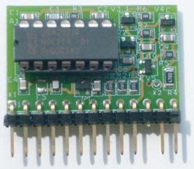
              3.1 Daughter board
                  The daughter board contains the UBA2021 IC with the preheat, sweep and oscillator
                  capacitors, the low voltage supply (VDD) components and some other low voltage
                  components.

                  The daughter PCB can easily be replaced if it becomes damaged. Care should be taken
                  that the board is inserted properly and to assist this, pin 11 has been removed from the
                  daughter board to prevent inserting the board incorrectly.

                                                                                                               019aaa283

                   Fig 2.   Daughter board
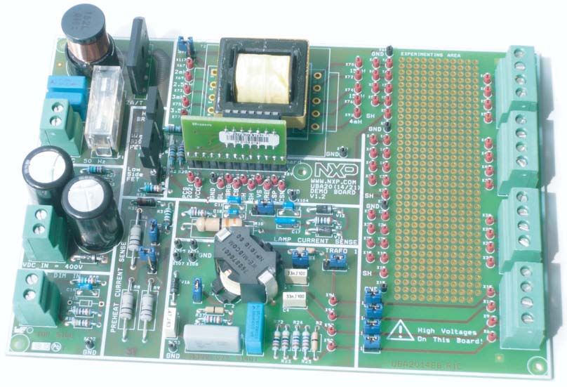
              3.2 Main board
                  The main board has been designed for both TL or CFL applications and comprises the
                  following:

                   •   DC and AC input connectors
                   •   Dimming input
                   •   Two sockets for FETs
                   •   Two different transformers
                   •   Area for experiments
                   •   Connectors for up to four burners

UM10412                           All information provided in this document is subject to legal disclaimers.                       © NXP B.V. 2010. All rights reserved.

User manual                                    Rev. 1 — 2 November 2010                                                                                     4 of 26
NXP Semiconductors                                                                                                       UM10412
                                                                                                                  UBA2021 evaluation board

                                                                                                                          019aaa289

 Fig 3.   UBA2014/21 Main board with UBA2021 daughter board inserted

UM10412                              All information provided in this document is subject to legal disclaimers.           © NXP B.V. 2010. All rights reserved.

User manual                                       Rev. 1 — 2 November 2010                                                                         5 of 26
NXP Semiconductors                                                                                                                                        UM10412
                                                                                                                                               UBA2021 evaluation board

4. Schematics
                           Figure 4 is a schematic of the daughter board with the UBA2021 IC. The component
                           values for the oscillator and sweep are RREF = 30 kΩ, CF = 100 pF, CP = 330 nF. These
                           values will give a minimum oscillator frequency of 39.5 kHz and a preheat time of 1.85 s.

                                          A1
               C1
          2            1     CI                        RHV               1 R1 2             1 R2 2        1 R8 2
                                  14              13                                                                                    Vbrg
              100 nF                                                         150 kΩ             150 kΩ         160 kΩ
                             CP                        G1
               C2
                                  8                2             GH
          2            1
                             CF                        S1
                                  12               3                                                                                    SH
          330 nF/16 V
                                                                                           C4
                           RREF                        FS                          1              2
               C3                 10               1
          2            1
                                       UBA2021P        G2                              100 nF                  1            1
              100 pF                               6             GL                                                             C6
                                                                                                                   C5
                                                                                                                                470 pF/
               R3                                      n.c.              X2
                                                                                                                   DNP
          1            2                           4                                                                            500 V
                                                                         TP                      V1            2            2
              30 kΩ        SGND                        VS       VDD                        1          2
                                  11               5
                                                                                1           BAS29         1                 1
                             RS                        PGND                         C7                        V2                C8
                                  9                7
                                                                                    1 μF/                     BAS29             1 nF/
                                                                                    25 V                                        100 V
                                                                                2                         2                 2
                                                                                                                                        PCS_2021      Pin 11 is cut off
                                                                         2    R4       1                                                            for correct insertion
                                                                 2                                                                                           X1
                                                                          47 Ω                            1                 1
                                                                     V3
                                                                     BAS29                                    C9            R5
                                                                                                                                                            1
                                                                 1                                            10 nF/        10 kΩ                           2
                                                                                                              50 V                                          3
                                                                 1                          E             2                 2
                                                                                  V4              B                                                         4
                                                                  R6          BC857C                                                                SH      5
                                                                  1 kΩ                                                                              GH      6
                                                                                            C                                                               7
                                                                 2                                                          C
                                                                                                                    B                              Vbrg     8
                                                                                                                            V5
                                                                                                                            BC847C
                                                                                                                                                    GL      9
                                                                                            1             1                                                 10
                                                                                                R7            C10           E                               11
                                                                                                3.3 kΩ        2.2 nF/
                                                                                                              100 V                                         12
                                                                                            2             2                                    PCS_2021     13
                                                                                                                                                          header 13
                                                                                                                                                               019aaa284

 Fig 4.   Daughter board with UBA2021 circuit

UM10412                                        All information provided in this document is subject to legal disclaimers.                                 © NXP B.V. 2010. All rights reserved.

User manual                                                 Rev. 1 — 2 November 2010                                                                                               6 of 26
xxxxxxxxxxxxxxxxxxxxx xxxxxxxxxxxxxxxxxxxxxxxxxx xxxxxxx x x x xxxxxxxxxxxxxxxxxxxxxxxxxxxxxx xxxxxxxxxxxxxxxxxxx xx xx xxxxx
                                                                                                                        xxxxxxxxxxxxxxxxxxxxxxxxxxx xxxxxxxxxxxxxxxxxxx xxxxxx xxxxxxxxxxxxxxxxxxxxxxxxxxxxxxxxxxx xxxxxxxxxxxx x x
                                                                                                                        xxxxxxxxxxxxxxxxxxxxx xxxxxxxxxxxxxxxxxxxxxxxxxxxxxx xxxxx xxxxxxxxxxxxxxxxxxxxxxxxxxxxxxxxxxxxxxxxxxxxxxxxxx xxxxxxxx
                                                                                                                        xxxxxxxxxxxxxxxxxxxxxxxxx xxxxxxxxxxxxxxxxxxxx xxx
User manual
                           UM10412

                                                                                                                                                                                                                                                                                                                                                                                                            NXP Semiconductors
                                                                                                                                                                                                   VDC
                                                                                                                                                                                                     1 R20 2
                                                                                                                                                                                                                                   Vbrg
                                                                                                                       connection for daughterboard                                                      220 kΩ
                                                                                                                                                                                                                                                                                           1 R22 2 1 R23 2 1 R24 2 1 R25 2
                                                                                                                                                       X89
                                                                                                                               1     CSN          1                                                                      placed in header                                                      43 kΩ          43 kΩ                 47 kΩ             47 kΩ
                                                                                                             X78 TP                                                            R1                          X2
                                                                                                                                                                          1           2              1                       D
                                                                                                                               1     CSP          2                  GH                                                                                                                                                    C1
                                                                                                             X79 TP                                                            33 Ω
                                                                                                                                                                                                                                                                                                                    1               2
                                                                                                                                                                                                     2                                    V3
                                                                                                                               1     Vref         3                                       1                                                                                                                  Cdc
                                                                                                             X80 TP                                                                                                      G                2SK3569                                     X114                          68 nF/400 V
                                                                                                                                                                                          R35        3                                                                                                                                        R2
                                                                                                                               1     LVS          4                                                                                                                                  header 2                                            2             1
                                                                                                             X81 TP                                                                       56 kΩ                               S
                                                                                                                                                                                                         socket 3                                                                                        Y5                                   0Ω
                                                                                                                               1     SH           5                                       2
                                                                                                             X82 TP                                                                                                                                                                                      jumper
                                                                                                                                                                                                                                                                                                                    T1 12
                                                                                                                               1     GH           6                                                                                                                                        1      2                                           C4                 1
                                                                                                             X83 TP                                                                                                                            SH                                                                                         1            2              X90 TP
                           All information provided in this document is subject to legal disclaimers.

                                                                                                                               1     PCS          7                                                                                                                                                           6            10                                    1
                                                                                                             X84 TP                                                                                                                                                                                                                      33 nF/100 V                  X92 TP
                                                                                                                               1     Vbrg         8                                                                                                                                   X115                                 9                                     1
                                                                                                             X85 TP                                                                                                                                                                                                                           C5                      X94 TP
                                                                                                                                                                                                                                                                                     header 2                 1                           1            2
                                                                                                                               1     GL           9                                                                                                                                                                                                              1
Rev. 1 — 2 November 2010

                                                                                                             X86 TP                                                                                                      placed in header                                                                                  7                                          X96 TP
                                                                                                                                                                               R3                          X14                                                                             2      1                                      33 nF/100 V
                                                                                                                               1                 10                       1           2              1                       D                                                                              760 870 401
                                                                                                             X87 TP                                                  GL                                                                                                                                  Y6
                                                                                                                                                 11                            33 Ω                  2                                                                                                   jumper                          2    R4       1
                                                                                                                                                                                          1                                               V6
                                                                                                                                                                                                                         G                2SK3569                                    1                                                        0Ω
                                                                                                                               1     VDD         12                                       R36        3                                                                                   C6
                                                                                                             X88 TP                                                                       56 kΩ                               S                                                          4.7 nF
                                                                                                                               1     PCS_2021 13                                                         socket 3
                                                                                                             X120 TP                                                                      2                                                                                              2000 V
                                                                                                                                                     socket 13                                                                      1 R37 2          1 R38 2                         2
                                                                                                                                                                                                                             LVS
                                                                                                                 connector position 11                                                                                                    0Ω            5.6 kΩ
                                                                                                                 glued sealed to prevent                             PCS_2021                                                                       1                1               1
                                                                                                                                                                                                     1     R5        2                                                                   C19
                                                                                                                 erroneous insertion of                                                                                                              R39                 V16
                                                                                                                                                                                                                                                                                         470 nF
                                                                                                                                                                                                                                                     1.2 kΩ              1N4937
                                                                                                                 daughterboard                                                                           8.2 kΩ                                                                          63 V
                                                                                                                                                                                                                                                    2                2               2
                                                                                                                                                                                          1         1                    X32
                                                                                                                                                                                                     R6
                                                                                                                                                                                                                  1
                                                                                                                                                                                          R31                                        Y7
                                                                                                                                                                                                     1Ω           2
                                                                                                                                                                                          1 kΩ                                       jumper
                                                                                                                                                                                                     2W                                                                     X33
                                                                                                                                                                                          2         2                header 2                                             header 3
                                                                                                                                                                                                                                                                                            Y8
                                                                                                                                   ground connections for                                                                X34                                                                jumper           lamp current sense circuit
                                                                                                                                                                                                                  1
                                                                                                                                    oscilloscope probes                       PCS                                                    Y9                                                                                                 V11                          X39
                                                                                                                                                                                                                  2                                                        1   2     3      1     R7     2                      1             2            LCS   1
                                                                                                                                                                                                                                     jumper
                                                                                                             X104 X105 X106 X107 X102 X108 X103 X109

                                                                                                                                                                                                                                                                                                                                                                                 UBA2021 evaluation board
                                                                                                                                                                                                                                                                                                  1 kΩ                                                           2
                                                                                                              TP   TP   TP   TP   TP   TP   TP   TP                                       1         1            1 header 2                    1                 1         CSN             1                  1                 1 1N4937          1
                                                                                                                                                                                                     R8          R9                                C18               C11                       C12                C17           R10                              3
                                                                                                                   1       1         1      1    1        1      1        1               R32                                                                                                                                                         V12
                                                                                                                                                                                                     1Ω          1Ω                                2.2 nF            10 nF                     1 nF               680 nF        33 Ω
                                                                                                                                                                                          100 kΩ                                                                                                                                                      1N4937
                                                                                                                                                                                                     2W          2W                                100 V             100 V                     100 V              50 V          2W                               header 3
                                                                                                                                                                                          2         2            2                             2                 2                         2                  2                 2                 2
                                                                                                                                                                                                                                                                                                                                                                      Y10

                                                                                                                                                                                                                                                                                                                                                                                                            UM10412
                                                                                                                                                                                                                                                                                                                                                                      jumper
                           © NXP B.V. 2010. All rights reserved.

                                                                                                                                                                                                                                                                                                                                                                     019aaa286
7 of 26

                                                                                                        Fig 5.         Main board half-bridge and resonance circuit - version R1C
NXP Semiconductors                                                                                                                                                 UM10412
                                                                                                                                                   UBA2021 evaluation board

                  VDC In = 400 V

                        X1                                                                                                     V1
                              1                                                                                           2         1                              VDC

                              2                                                                                           1N4937                               2
                                                                                                                                                               R27
                  MKDS 2.5/2-5.08                                                                                                                              75 kΩ
                                                                                                                                                  1
                                                                                                                                                      C16      1
                                                                                                                                                      47 μF/
                                                                                                                      2    V2                         350 V    2
                                                                                                                          GBU8K                   2            R33
                                                                                                                                                               75 kΩ
               VAC In = 230 V 50 Hz                                      L1
                                               F1                                2                     4                            1                          1
                                                                    1
                        X3             Fuseholder 5x20                  1.5 mH                                                                                 2
                              1                                1                       1
                                                                   C2                      C3                                                                  R29
                                                                   47 nF/                  47 nF/                                                 1            75 kΩ
                              2
                                                                   305 Vac                 305 Vac                    3                               C15      1
                  MKDS 2.5/2-5.08
                                                               2                       2                                                              47 μF/
                                                                                                                                                      350 V    2
                                                                                                                                                  2            R34
                                       F2                                                                                                                      75 kΩ
                                                     Y12
                                       2A            Cover                                                                                                     1

                                                                                                                                                               019aaa287

 Fig 6.   Main board input section

                                                External
                                            dimming voltage               1 R40 2                                                   VDD
                                               0 V to 10 V                    75 kΩ

                                                    X68
                                                          1               1 R18 2                                                   CSP
                                                           2                  33 kΩ           1             1             1
                                                                                                                              C14
                                                                                              R19               V15
                                            MKDS 2.5/2-5.08                                                                   10 nF/
                                                                                              11 kΩ             DNP
                                                                                                                              100 V
                                                                                              2             2             2

                                                                                                                               019aaa285

 Fig 7.   Main board dimming input (only in combination with UBA2014 daughter board)

                                              X117
                                             header 2
                                                           Y11
                                                           jumper
                                               1     2
                                  SH
                                                                   1      X67                     1 T2
                                                    X67 TP                                                  10            X70           1
                                                                                     2 mH
                                                                                                                                              X70 TP
                                                                   1      X69                     2              15 μH
                                                    X69 TP                                                  9             X72           1
                                                                                     2.5 mH
                                                                                                                                              X72 TP
                                                                   1      X73                     3
                                                    X73 TP
                                                                                     3 mH                   8             X74           1
                                                                   1      X75                     4                                           X74 TP
                                                    X75 TP                                                       15 μH
                                                                                     3.5 mH                 7             X76           1
                                                                   1      X77                     5                                           X76 TP
                                                    X77 TP
                                                                                     4 mH
                                                                   1      X91                     6
                                                    X91 TP
                                                                                                      DNP                                   019aaa300

 Fig 8.   Main board transformer T2/T3

UM10412                                              All information provided in this document is subject to legal disclaimers.                                    © NXP B.V. 2010. All rights reserved.

User manual                                                         Rev. 1 — 2 November 2010                                                                                                8 of 26
NXP Semiconductors                                                                                                                                   UM10412
                                                                                                                                         UBA2021 evaluation board

                                    X110          X111             X112         X113
                                   header 2      header 2         header 2     header 2                      Y1           Y2
                                                                                                             jumper       jumper
                                                                                                             Y3           Y4
                                     1   2           1    2         1    2         1                2        jumper       jumper

                                                                                                                                      LAMP 4
                                                                                                                                         X8
                               1                                                                                      1              1
                                     X90 TP                                                                  X6 TP
                               1                                                                                      1              2
                                     X92 TP                                                                  X9 TP
                               1                                                                                      1              3
                                     X94 TP                                                                 X11 TP

                                                                                       EXPERIMENTING AREA
                               1                                                                                      1              4
                                     X96 TP                                                                 X13 TP
                                                              1                                                                    MKDS 2.2/4-5.08
                                                                    X15 TP

                                                      SH
                                                              1                                                                       LAMP 3
                                                                    X17 TP                                                               X21
                                                              1                                                       1              1
                                     X18 TP                         X19 TP                                  X20 TP
                                                              1                                                       1              2
                                     X22 TP                         X23 TP                                  X24 TP
                                                              1                                                       1              3
                                     X25 TP                         X26 TP                                  X27 TP
                                                              1                                                       1              4
                                     X28 TP                         X29 TP                                  X30 TP
                                                              1                                                                    MKDS 2.2/4-5.08
                                                                    X31 TP

                                                     SH
                                                            1                                                                         LAMP 2
                                                                   X35 TP                                                                X42
                                                            1                                                         1              1
                                    X36 TP                         X37 TP                                   X38 TP
                                                            1                                                         1              2
                                    X43 TP                         X40 TP                                   X41 TP
                                                            1                                                         1              3
                                    X44 TP                         X45 TP                                   X46 TP
                                                                                       EXPERIMENTING AREA

                                                            1                                                         1              4
                                    X47 TP                         X48 TP                                   X49 TP
                                                            1                                                                      MKDS 2.2/4-5.08
                                                                   X50 TP

                                                     SH
                                                              1                                                                       LAMP 1
                                                                   X52 TP                                                                X56
                                                              1                                                       1              1
                                    X53 TP                         X54 TP                                   X55 TP
                                                              1                                                       1              2
                                    X57 TP                         X58 TP                                   X59 TP
                                                              1                                                       1              3
                                    X60 TP                         X61 TP                                   X62 TP
                                                              1                                                       1              4
                                    X63 TP                         X64 TP                                   X65 TP
                                                              1                                                                    MKDS 2.2/4-5.08
                                                                   X66 TP
                                                                                                                                       019aaa288

 Fig 9.   Main board lamp connectors and experimental area

UM10412                                       All information provided in this document is subject to legal disclaimers.                             © NXP B.V. 2010. All rights reserved.

User manual                                                Rev. 1 — 2 November 2010                                                                                           9 of 26
NXP Semiconductors                                                                                                    UM10412
                                                                                                               UBA2021 evaluation board

5. Connectors

              5.1 Power supply connectors
                  The board can be supplied by either a high voltage DC or a mains AC input. For most
                  applications the high voltage DC input should be used. In the final product, a PFC of
                  choice may be used to replace the high voltage DC supply.
                  For some applications (such as CFL applications) the rectified mains is sufficient. In these
                  cases a mains input of 230 V AC may be used.

                  Table 1.    DC high voltage input connector X1
                  Connector                 Signal                                   Comment
                  X1-1                      +                                        + 400 V DC in
                  X1-2                      GND                                      Ground

                  Table 2.    AC input connector X3
                  Connector                 Signal                                   Comment
                  X3-1                      ~                                        Mains 230 V AC
                  X3-2                      ~                                        Mains 230 V AC

              5.2 Dimming input
                  The UBA2021 does not have dimming functionality so this input is not used. If dimming is
                  required, please use the UBA2014.

              5.3 Lamp connectors
                  There are four lamp connectors on the board. The connectors are listed in Table 3,
                  Table 4, Table 5 and Table 6, together with the names of the test points that are connected
                  to them.

                  Table 3.    Lamp 1 (X56)
                  TP                                             Comment
                  X55                                            connection for filament 1
                  X59                                            connection for filament 1
                  X62                                            connection for filament 2
                  X65                                            connection for filament 2

                  Table 4.    Lamp 2 (X42)
                  TP                                             Comment
                  X38                                            connection for filament 1
                  X41                                            connection for filament 1
                  X46                                            connection for filament 2
                  X49                                            connection for filament 2

UM10412                           All information provided in this document is subject to legal disclaimers.           © NXP B.V. 2010. All rights reserved.

User manual                                     Rev. 1 — 2 November 2010                                                                      10 of 26
NXP Semiconductors                                                                                                   UM10412
                                                                                                              UBA2021 evaluation board

                  Table 5.   Lamp 3 (X21)
                  TP                                            Comment
                  X20                                           connection for filament 1
                  X24                                           connection for filament 1
                  X27                                           connection for filament 2
                  X30                                           connection for filament 2

                  Table 6.   Lamp 4 (X8)
                  TP                                            Comment
                  X6                                            connection for filament 1
                  X9                                            connection for filament 1
                  X11                                           connection for filament 2
                  X13                                           connection for filament 2

              5.4 Test points
                  Eight black ground pins (X102 to X109) are distributed over the board so that
                  (oscilloscope) probes can be grounded without the need for long grounding wires.

                  Remark: A test pin is available for each pin of the daughter board.

                  Table 7.   Connections of the daughter board
                  Test Pin      Name                        Comment
                  X78           CSN                         negative input for the average current sensor for UBA2014
                                                            daughter board
                  X79           CSP                         positive input for the average current sensor for UBA2014
                                                            daughter board
                  X80           Vref                        reference voltage output for UBA2014 daughter board
                  X81           LVS                         lamp voltage sensor input for UBA2014 daughter board
                  X82           SH                          source for the high-side switch
                  X83           GH                          gate output for the high-side switch
                  X84           PCS                         preheat current sensor input for UBA2014 daughter board
                  X85           Vbrg                        Connection to VDC via R20 (220 kΩ)
                  X86           GL                          gate output for the low-side switch
                  X87           GND                         ground
                  X88           VDD                         low voltage supply
                  X120          PCS_2021                    preheat current sense for the UBA2021 daughter board

UM10412                          All information provided in this document is subject to legal disclaimers.           © NXP B.V. 2010. All rights reserved.

User manual                                   Rev. 1 — 2 November 2010                                                                       11 of 26
NXP Semiconductors                                                                                                          UM10412
                                                                                                                   UBA2021 evaluation board

               5.5 Transformer T1
                    In the default setup, transformer T1 will be used and is connected with jumpers to lamp
                    connector 4 (X 8). The transformer specifications are listed in Section 6.

                    Table 8.      Default connection transformer T1
                    Header                          Comment
                    X110                            Insert to connect T1 to filament 1, lamp 4
                    X111                            Insert to connect T1 to filament 1, lamp 4
                    X112                            Insert to connect T1 to filament 2, lamp 4
                    X113                            Insert to connect T1 to filament 2, lamp 4
                    X114                            Insert to connect SH to transformer T1
                    X115                            Insert to connect T1 to resonant capacitor C6 (4.7 nF, 2000 V)

               5.6 FET
                    Two NMOST FETs should be placed in X2 and X14. The supplied NMOST's are Toshiba
                    2SK3569 (VDS = 600 V; ID = 10 A; RDSon = 0.54 Ω). When using different NMOS types, the
                    values of gate resistors R1 and R3 (default 33 Ω) maybe changed.

               5.7 Current sense selection
                    A feed forward mechanism in the UBA2021 ensures that the lamp power will not increase
                    above the maximum allowed value due to an increased mains voltage. This means that
                    the operating frequency is controlled by the bus voltage rather than by the lamp current or
                    the half-bridge current.

                    Table 9.      Current sensing selection
                    X33                                             pins 1 and 2                                   pins 2 and 3
                    half-bridge                                     open                                           open
                    lamp current                                    open                                           open

              5.7.1 Half-bridge current sensing
                    The half-bridge current is sensed for controlling the preheat current. Different values of
                    the sense resistor can be selected using jumpers X32 and X34. To connect the lamp to
                    ground, X39 should be shorted between pin 2 and pin 3.

                    Table 10.     Current sensing selection
                    X32                                             X34                                            Resistance
                    short                                           short                                          0.5 Ω
                    short                                           open                                           1.0 Ω
                    open                                            short                                          1.5 Ω
                    open                                            open                                           2.0 Ω

              5.7.2 Lamp current sensing
                    The UBA2021 does not sense the lamp current, so X39 should be shorted between pin 2
                    and pin 3 in order to connect the lamp to ground.

UM10412                               All information provided in this document is subject to legal disclaimers.                © NXP B.V. 2010. All rights reserved.

User manual                                        Rev. 1 — 2 November 2010                                                                            12 of 26
NXP Semiconductors                                                                                                    UM10412
                                                                                                               UBA2021 evaluation board

              5.8 Using transformer T3
                  The jumper X117 should be inserted to use the flexible transformer T3. This will connect
                  SH to pin 1 of the transformer. Table 11 shows the different inductance values. The
                  specifications of the transformer are listed in Section 6.

                  Table 11.   Transformer T3 primary connections - Inductance to pin 1 (X67)
                  Connection                                                                   Inductance
                  X69                                                                          2.0 mH
                  X73                                                                          2.5 mH
                  X75                                                                          3.0 mH
                  X77                                                                          3.5 mH
                  X91                                                                          4.0 mH

                  Table 12.   Transformer T3 secondary connections
                  Connection                                                                   Inductance
                  X70-X72                                                                      15 μH
                  X74-X76                                                                      15 μH

                  Transformer T3 has a double footprint that enables the use of different types of
                  transformers. The transformers are referred to as T2 and T3 on the schematic drawings.

UM10412                           All information provided in this document is subject to legal disclaimers.           © NXP B.V. 2010. All rights reserved.

User manual                                    Rev. 1 — 2 November 2010                                                                       13 of 26
NXP Semiconductors                                                                                                                     UM10412
                                                                                                                              UBA2021 evaluation board

6. Transformer specifications

               6.1 Transformer T1

              6.1.1 Schematic diagram
                     • Manufacturer: Würth Elektronik
                     • Part number: 760870401

                                                                                                                   12
                                                                                                         N3
                                                                              1
                                                                                                                   10
                                                                                   N1
                                                                                                                   9
                                                                              6
                                                                                                         N2

                                                                                                                   7
                                                                                                     019aaa301

                     Fig 10. Transformer T1 schematic diagram

              6.1.2 Winding specification
                    Table 13.    Electrical characteristics for transformer T1
                    Properties                          Test conditions                                                 Value          Unit          Tolerance
                    Inductance N1                       50 kHz/0.1 V                                          L0        2.9            mH            ±5%
                    Turns ratio N1 - N5                 N1: N2: N3                                            TR        26.1 : 1 : 1                 ±3%
                    DC-resistance N1                    at 20 °C                                              RDC1      2.7            Ω             maximum
                    DC-resistance N2                    at 20 °C                                              RDC2      180            mΩ            maximum
                    DC-resistance N3                    at 20 °C                                              RDC3      180            mΩ            maximum
                    Saturation current N1               dL/L=20 %                                             ISAT      1.6            A             typical
                    Leakage inductance N1               200 kHz/0.1 V rest shorted LS                                   350            μH            maximum
                    Coupling capacitance                20 kHz/1 V all windings                               CWW       11.0           pF            typical
                    Hipot test                          3 mA, 1s all windings                                 HV        1.2            kV

              6.1.3 Dimensions
                     • Core: RM-8 (Ferroxcube RM/I or equivalent)
                     • Core material: 3F3, N87 or equivalent
                     • Bobbin: RM-8 (12 pin, vertical type)

UM10412                               All information provided in this document is subject to legal disclaimers.                       © NXP B.V. 2010. All rights reserved.

User manual                                        Rev. 1 — 2 November 2010                                                                                   14 of 26
NXP Semiconductors                                                                                                                        UM10412
                                                                                                                                   UBA2021 evaluation board

                                                               12
                                                          11
                                                          10        1

                                                               3    2

                                                                                                                                                 21.59 mm
                                                                                                                                                   (max)
                                    8    9

                                   7         4
                                             5
                                         6

                                             21.59 mm                                            17.27 mm
                                               (max)                                               (max)                                          019aaa251

                           Fig 11. Transformer T1

                   6.2 Transformer T3

                 6.2.1 Schematic diagram
                           • Manufacturer: Würth Elektronik
                           • Part number: 760870402

                                                                                                                              10
                                                                                         1
                                                                                              N1                    N7
                                                                                         2
                                                                                              N2
                                                                                         3                                    9
                                                                                              N3
                                                                                         4                                    8
                                                                                              N4
                                                                                         5
                                                                                              N5                    N6
                                                                                         6
                                                                                                                              7
                                                                                                                019aaa302

                           Fig 12. Transformer T3 schematic diagram

Table 14.    Electrical characteristics for transformer T3
Properties                    Test conditions                                                       Value                                   Unit          Tolerance
InductanceN1-N5               50 kHz/0.1 V                                          L0              4.0                                     mH            ±5%
Turns ratio N1 - N5           N1: N2: N3: N4: N5: N6: N7                            TR              12 : 1.33, 1.25 : 1.17, 1.17 : 1:1                    ±3%
DC-resistance N1-N5           at 20 °C                                              RDC1-5 1.85                                             Ω             ± 20 %
DC-resistanceN6               at 20 °C                                              RDC6            135                                     mΩ            ± 20 %
DC-resistance N7              at 20 °C                                              RDC7            140                                     mΩ            ± 20 %
Saturation current N1-N5      dL/L = 20 %                                           ISAT            1.0                                     A             typical
Leakage inductance N1-N5      200 kHz/0.1 V rest shorted                            LS              275                                     μH            typical
Coupling capacitance          20 kHz/1 V all windings                               CWW             30.0                                    pF            typical
Hipot test                    3 mA, 1 s all windings                                HV              3.0                                     kV

UM10412                                          All information provided in this document is subject to legal disclaimers.                © NXP B.V. 2010. All rights reserved.

User manual                                                    Rev. 1 — 2 November 2010                                                                           15 of 26
NXP Semiconductors                                                                                                     UM10412
                                                                                                                UBA2021 evaluation board

              6.2.2 Dimensions

                             10                      1

                                                                                                                                31.5 mm
                                                                                                                                 (max)

                              6                      5

                                   31.5 mm                                             21 mm
                                    (max)                                              (max)                                   019aaa299

                    Fig 13. Transformer T3

                    •   Core: E30/15/7
                    •   Core material: Ferrite
                    •   Air gap in center leg: 1100 μm
                    •   Bobbin: CSH-E30/7-1S-10P

UM10412                            All information provided in this document is subject to legal disclaimers.           © NXP B.V. 2010. All rights reserved.

User manual                                     Rev. 1 — 2 November 2010                                                                       16 of 26
NXP Semiconductors                                                                                                            UM10412
                                                                                                                   UBA2021 evaluation board

7. Application example

              7.1 Default application T5 HE 35 W
                  The default settings of the board are for a T5 HE 35 W burner.

                  Table 15.   Default settings
                  Jumper                              Position                                     Comment
                  X32                                short                                         half-bridge sense resistor 1 Ω (used for PCS)
                  X34                                 open                                         -
                  X33                                 1-2 open, 2-3 short                          use lamp current sensing
                  X114                                short                                        connect transformer T1
                  X115                                short                                        -
                  X39                                 1-2 shorted, 2-3 open                        connect lamp to lamp current sense circuit
                  X110, X111, X112, X113 short                                                     connect to lamp 4
                  X117                               open                                          do not connect transformer T3

                  Table 16.   External connections for T5 HE 35W
                  Jumper      Position                      Comment
                  X1          VDC                           400 V DC
                  X68         External dimming the UBA2021 board has no dimming so this input can be left open.
                  X8          burner                        T5 HE 35 W burner

UM10412                             All information provided in this document is subject to legal disclaimers.                © NXP B.V. 2010. All rights reserved.

User manual                                      Rev. 1 — 2 November 2010                                                                            17 of 26
NXP Semiconductors                                                                                                  UM10412
                                                                                                             UBA2021 evaluation board

8. Bill of Materials (BOM)
              Table 17.     BOM daughter board
               Reference             Value or type no.                                 Component
               A1                    UBA2021P                                          NXP Semiconductors UBA2021P IC
               C1, C4                100 nF/50 V                                       Capacitor ceramic X7R, 50 V, 10 %
               C2                    330 nF/16 V                                       Capacitor ceramic X7R, 16 V, 10 %
               C3                    100 pF/100 V                                      Capacitor ceramic C0G, 50 V, 1 %
               C5                    n.m.                                              -
               C6                    470 pF/500 V                                      Capacitor ceramic 500 V NP0 5 %
               C7                    1 μF/25 V                                        Capacitor ceramic X7R 25 V, 10 %
               C8                    1 nF/100 V                                       Capacitor ceramic X7R 100 V, 10 %
               C9                    10 n                                              Capacitor ceramic X7R, 50 V, 10 %
               C10                   2.2 n / 100 V                                     Capacitor ceramic X7R 100 V, 10 %
               R1, R2                150 kΩ                                            Resistor 1 % 0.125 W 100 ppm RC12H
               R3                    30 kΩ                                             Resistor 1 % 0.125 W 100 ppm RC12H
               R4                    47 Ω                                              Resistor 1 % 0.125 W 0 to +500 ppm RC12H
               R5                    10 kΩ                                             Resistor 1 % 0.125 W 100 ppm RC12H
               R6                    1 kΩ                                              Resistor 1 % 0.125 W 100 ppm RC12H
               R7                    3.3 kΩ                                            Resistor 1 % 0.125 W 100 ppm RC12H
               R8                    160 kΩ                                            Resistor 1 % 0.125 W 100 ppm RC12H
               V1, V2, V3            BAS29                                             NXP Semiconductors, Diode, 50 ns 90 V 250 mA
               V4                    BC857C                                            NXP Semiconductors, PNP transistor
               V5                    BC847C                                            NXP Semiconductors, NPN transistor

UM10412                         All information provided in this document is subject to legal disclaimers.           © NXP B.V. 2010. All rights reserved.

User manual                                  Rev. 1 — 2 November 2010                                                                       18 of 26
NXP Semiconductors                                                                                                    UM10412
                                                                                                             UBA2021 evaluation board

              Table 18.     BOM main board
               Reference                           Value or type no.                     Component
               C1                                  68 nF/400 V                           Capacitor MKT 400 V DC 10 %
               C2, C3                              47 nF/305 V AC                        Capacitor, MKP Class X2 20 %
               C4, C5                              33 nF/100 V                           Capacitor MKT 100 V DC 5 %
               C6                                  4.7 nF/2000 V                         Capacitor MKP radial potted, 5 %
               C11, C14                            10 nF/100 V                           Capacitor ceramic disc X7R, 10 %
               C12                                 1 nF/100 V                            Capacitor ceramic disc X7R, 10 %
               C15, C16                            47 μF/350 V                           Capacitor elco rad 350 V 105 °C 20 %
               C17                                 680 nF/50 V                           Capacitor ceramic disc X7R, 10 %
               C18                                 2.2 nF/100 V                          Capacitor ceramic disc X7R, 10 %
               C19                                 470 n/63 V                            Capacitor MKT 63 V DC 5 %
               F1                                  Fuse holder 5 x 20 Fuse holder for 5 mm x 20 mm fuses
               F2                                  2A                                    Fuse 5 mm x 20 mm time lag
               L1                                  1.5 mH                                Inductor Choke Ir = 850 mA, R= 580 mΩ
               R1, R3                              33 Ω                                  Resistor 1 % 0.6 W 50 ppm MRS25
               R2, R4                              0Ω                                    Zero Ohm Link Im= 25 A at 25 °C
               R5                                  8.2 KΩ                                Resistor 1 % 0.6 W 50 ppm MRS25
               R6, R8, R9                          1Ω2W                                  Resistor Power 5 % 2 W 100 ppm/°C MFP
               R7                                  1 KΩ                                  Resistor 1 % 0.6 W 50 ppm MRS25
               R10                                 33 Ω 2 W                              Resistor Power 5 % 2 W 450 ppm/°C Carbon Film
               R18                                 33 kΩ                                 Resistor 1 % 0.6 W 50 ppm MRS25
               R19                                 11 kΩ                                 Resistor 1 % 0.6 W 50 ppm MRS25
               R20                                 220 kΩ                                Resistor 1 % 0.6 W 50 ppm MRS25
               R22, R23                            43 kΩ                                 Resistor 1 % 0.6 W 50 ppm MRS25
               R24, R25                            47 kΩ                                 Resistor 1 % 0.6 W 50 ppm MRS25
               R27, R29, R33, R34                  75 kΩ                                 Resistor 1 % 0.6 W 50 ppm MRS25
               R31                                 1.0 kΩ                                Resistor 1% 0.6 W 50 ppm MRS25
               R32                                 100 kΩ                                Resistor 1% 0.6 W 50 ppm MRS25
               R35, R36                            56 kΩ                                 Resistor 1% 0.6 W 50 ppm MRS25
               R37                                 0Ω                                    Zero Ohm Link Im = 25 A at 25 °C
               R38                                 5.6 kΩ                                Resistor 1 % 0.6 W 50 ppm MRS25
               R39                                 1.2 kΩ                                Resistor 1 % 0.6 W 50 ppm MRS25
               R40                                 75 kΩ                                 Resistor 1 % 0.6 W 50 ppm MRS25
               T1                                  760870401                             Würth Elektronik Part number: 760870401
               T3                                  760870402                             Würth Elektronik Part number: 760870402
               V1, V11, V12, V16                   1N4937                                Diode, fast recovery, 600 V, 1 A
               V2                                  GBU8K                                 BRIDGE 800 V, 8 A TH
               V3, V6                              2SK3569                               MOSFET N-ch 600 V 10 A 0.54 Ω
               V15                                 n.m.                                  -
               X1, X3, X68                         MKDS 2,5/2-5,08                       Terminal block (screw) 2-pole, p = 2e, 2.5 mm2
               X2, X14                             Socket 3                              Socket straight p = 2.54, h = 7 mm
               X8, X21, X42, X56                   MKDS 2,5/4-5,08                       Terminal block (screw) 4-pole, p = 2e, 2.5 mm2
UM10412                         All information provided in this document is subject to legal disclaimers.              © NXP B.V. 2010. All rights reserved.

User manual                                  Rev. 1 — 2 November 2010                                                                          19 of 26
NXP Semiconductors                                                                                                                                       UM10412
                                                                                                                                               UBA2021 evaluation board

9. Layout

               T                                                                                                                                    R1A
                                                             019aaa291                                                                                             019aaa290

            Top view                                                                                          Bottom view
 Fig 14. Daughter PCB layout

                                                                                                                  V1        V3
                                                                                                                                       C7 C6   C5
                   C1   C3   R1                                                                               3
          C2

                                                                                                              1
                                                                   C8                                             V2    2   V4     3
                                  R7       V5                                                                 3
                   R6 C10 R5
                                       1              R3
                   C9                                                                                                              3
                                                C11                                                                                            C4   A1
                                                                                                                    1       2          R4
          1 X1                              3                      R2

                                                             019aaa292                                                                                             019aaa296

            Top view                                                                                          Bottom view
 Fig 15. Daughter board silk screen

UM10412                                               All information provided in this document is subject to legal disclaimers.                          © NXP B.V. 2010. All rights reserved.

User manual                                                        Rev. 1 — 2 November 2010                                                                                      20 of 26
NXP Semiconductors                                                                                                               UM10412
                                                                                                                        UBA2021 evaluation board

              TOP SIDE
                                         3322 029 91481                                                          UBA2014EB R1C
                                                                                                                                          019aaa295

 Fig 16. UBA2014/21 main board PCB layout top view

UM10412                             All information provided in this document is subject to legal disclaimers.                   © NXP B.V. 2010. All rights reserved.

User manual                                      Rev. 1 — 2 November 2010                                                                               21 of 26
NXP Semiconductors                                                                                                     UM10412
                                                                                                                UBA2021 evaluation board

                                                                                                                      BOTTOM SIDE
                                                                                                                        B

                                                                                                                                 019aaa293

 Fig 17. UBA2014/21 main board PCB layout bottom view

UM10412                            All information provided in this document is subject to legal disclaimers.           © NXP B.V. 2010. All rights reserved.

User manual                                     Rev. 1 — 2 November 2010                                                                       22 of 26
xxxxxxxxxxxxxxxxxxxxx xxxxxxxxxxxxxxxxxxxxxxxxxx xxxxxxx x x x xxxxxxxxxxxxxxxxxxxxxxxxxxxxxx xxxxxxxxxxxxxxxxxxx xx xx xxxxx
                                                                                                                      xxxxxxxxxxxxxxxxxxxxxxxxxxx xxxxxxxxxxxxxxxxxxx xxxxxx xxxxxxxxxxxxxxxxxxxxxxxxxxxxxxxxxxx xxxxxxxxxxxx x x
                                                                                                                      xxxxxxxxxxxxxxxxxxxxx xxxxxxxxxxxxxxxxxxxxxxxxxxxxxx xxxxx xxxxxxxxxxxxxxxxxxxxxxxxxxxxxxxxxxxxxxxxxxxxxxxxxx xxxxxxxx
                                                                                                                      xxxxxxxxxxxxxxxxxxxxxxxxx xxxxxxxxxxxxxxxxxxxx xxx
User manual
                           UM10412

                                                                                                                                                                                                                                                                                                                                                                                                                                                          NXP Semiconductors
                                                                                                                                                                                                                                                                                                                                                                 X66
                                                                                                                     L1                                                                                     1        T2                                                                                                                                                     EXPERIMENTING AREA
                                                                                                                                                 V2                                                                                                                                                                                                            GND
                                                                                                                                                                                                     SH
                                                                                                                                                                                                                                                                                                                                                           X63        X64

                                                                                                                                                                                                    X117                                                                                                                                      X70
                                                                                                                                                                                                                                   T3                                                                                                                                                                    X56   LAMP 1
                                                                                                                                                                                                     X67                                                                                                                                           15 μH   X60        X61                          X65

                                                                                                                                                                                                     2 mH                                                                                                                                     X72

                                                                                                                                                                                                                                                                                                                     10

                                                                                                                                                                                                                                                                                                                          10
                                                                                                                                                                                                                               1

                                                                                                                                                                                                                                          1
                                                                                                                                                                                                     X69                                                                                                                                                   X57        X58                          X62

                                                                                                                                                                                                  2.5 mH                                                                                                                                      X74

                                                                                                                                                                                                                               2

                                                                                                                                                                                                                                          2

                                                                                                                                                                                                                                                                                                                     9

                                                                                                                                                                                                                                                                                                                          9
                                                                                                                                                                                                     X73                                                                                                                                           15 μH   X53        X54                          X59
                                                                                                             C3
                                                                                                                                                                                                     3 mH                                                                                                                                     X76

                                                                                                                                                                                                                               3

                                                                                                                                                                                                                                          3

                                                                                                                                                                                                                                                                                                                     8

                                                                                                                                                                                                                                                                                                                          8
                                                                                                                                                  2 A/T                                              X75                                                                                                                                                              X52                          X55

                                                                                                             C2                                                                                   3.5 mH                                                                                                                                      X91          SH

                                                                                                                                                                                                                               4

                                                                                                                                                                                                                                          4

                                                                                                                                                                                                                                                                                                                     7

                                                                                                                                                                                                                                                                                                                          7
                                                                                                                                                                            HALF

                                                                                                                                                                                                                                                                                                                                                                                                               1
                                                                                                                                                                                                     X77                                                                                                                                           4 mH               X50
                                                                                                                                                                           BRIDGE
                                                                                                                                                                                                                                                                                                                                                           GND                                           X42   LAMP 2

                                                                                                                                                                                                                               5

                                                                                                                                                                                                                                          5

                                                                                                                                                                                                                                                                                                                     6

                                                                                                                                                                                                                                                                                                                          6
                                                                                                             X3                                                                                                                                                                                                                                            X47        X48                          X49
                                                                                                                      1

                                                                                                                                                                                           1                    R1
                                                                                                                                                                                                 g
                                                                                                                                                      High
                                                                                                                                                      Side                                                                                                                                                                                  X109           X44        X45                          X46
                                                                                                                                                                                                 d
                                                                                                                                                      FET
                           All information provided in this document is subject to legal disclaimers.

                                                                                                                                                                                                                                                                                                                                     GND
                                                                                                                                                                                                 s
                                                                                                                                                                               R35         X2                                                                                                                                                              X40        X43                          X41
                                                                                                                                                 F1                                                                              UBA20 (14/21) Daughter Board
                                                                                                                   230 VAC 50 Hz                                                           1                                                                                                                1
                                                                                                                                                                                                 g
Rev. 1 — 2 November 2010

                                                                                                                                                                                                                                                                                                        X89                                                X36        X37                          X38
                                                                                                                                                      Low                                             R3 R20 X120                   X87             X85           X83         X81              X79

                                                                                                                                                                                                                                              X86

                                                                                                                                                                                                                                                            X84

                                                                                                                                                                                                                                                                        X82

                                                                                                                                                                                                                                                                                        X80

                                                                                                                                                                                                                                                                                                      X78
                                                                                                                                           R27
                                                                                                                                                      Side                                       d              X88                                                                                                            WWW.NXP.COM
                                                                                                            R34
                                                                                                                                                      FET                                                                                                                                                                      UBA20 (14/21)

                                                                                                                                                                                                                                                                                                                                                                                                               1
                                                                                                                                                                                                                                                                                                                                                                      X35
                                                                                                                                                                                     X14         s                                                                                                                             DEMO BOARD

                                                                                                                                                                                                                                                     VBRG
                                                                                                            R29                            R33                                                                                                                                                                  GND

                                                                                                                                                                                                                                                                                        VREF
                                                                                                                                                                                                                                                                                                                                                           SH
                                                                                                                                                                                                                 2021

                                                                                                                                                                                                                                        GND
                                                                                                                                                                                                                           VCC

                                                                                                                                                                                                                                                                                                      CSN
                                                                                                                                                                                                                 PCS

                                                                                                                                                                                                                                                            PCS

                                                                                                                                                                                                                                                                                                CSP
                                                                                                                                                                                                                                                                              LVS
                                                                                                                                                                                                                                                                                                                               V1.2

                                                                                                                                                                                                                                                                  GH
                                                                                                                                                                                                                                                                        SH
                                                                                                                               C15

                                                                                                                                                                                                                                               GL
                                                                                                                                                                                                                                                                                                                                                                  X31
                                                                                                                                                                               R36                                                                                                                                   X104
                                                                                                                                                                                                                                                                                                                                                               GND                                       X21   LAMP 3
                                                                                                                                                                                                                                              C11                                   X33                          C12                                       X28    X29                              X30
                                                                                                                                         C16                                                                              R5              C18                           1
                                                                                                                                                                       R32                                                                                                                                                                  V12
                                                                                                                                                                                                R31
                                                                                                                                                                                                                                                                                                                                                           X25    X26                              X27
                                                                                                                                                                                     R6
                                                                                                                                                                                                                                                                              R10                                                           R7
                                                                                                                                                                                                X32                                                                                                              C17
                                                                                                                                                                                                1

                                                                                                             X1                                                                                                                                                                                                                             V11            X22    X23                              X24
                                                                                                                                                                                                                                                                                                            LAMP CURRENT SENSE
                                                                                                                      1

                                                                                                                                                                                                                                                    T1                              8          7
                                                                                                                                                                                                                                                                                                                                        TRAFO 1            X18    X19                              X20
                                                                                                                                                                                                                X105       X106
                                                                                                                                                       PREHEAT CURRENT SENSE

                                                                                                                                                                                                X34                                GND                                                                  6            X114      R4     X39
                                                                                                                                                                                                1

                                                                                                                                                                                                                                                                                                                                                                                                               1
                                                                                                                                           V1                                                                                                                                                                                                       1             X17
                                                                                                                                                                                                                                                                                                            5
                                                                                                                                                                                                                X107       X108
                                                                                                                                                                                                                                                                                                                     SH                                    SH                                            X8    LAMP 4
                                                                                                              VDC_IN = 400 V
                                                                                                                                                                                                                                                                                                                                                                  X15                              X13
                                                                                                             ANALOG DIM IN               R40                                                                          V16                                                                                                                                      GND
                                                                                                                                                                                                                                 X115         11                                                                C5
                                                                                                                                                                                     R8              R9                                                                                                                                 X96                    X113                                X11
                                                                                                                  0 - 10 V                                                                                                                    12
                                                                                                             X68               C14                                                                                                                                                                                                                         1
                                                                                                                      1

                                                                                                                                                                                                                                                                                                                                                                                                                               UBA2021 evaluation board
                                                                                                                                   V15                                                                                                                      1     2                                                                     X94                    X112                                X9
                                                                                                                                                                                                                                                                                                                C4
                                                                                                                                                                                                                                                                               C1                                                                          1
                                                                                                                                   R19                                                                                              R37
                                                                                                                                                                                                                X103
                                                                                                                                                                                                                                                                                                      R22              R24           R2 X92                    X111              High Voltages     X6
                                                                                                                                   R18                                                                                              R39                                                                                                                    1                     On This Board !
                                                                                                                                                                                                                                                                        C6

                                                                                                                                                                                                                                                                                                                                                                                                               1
                                                                                                                                                                                                                                    R38                                                                                                 X90                    X110

                                                                                                                                                                                                                                                                                                                                                                                                                                                          UM10412
                           © NXP B.V. 2010. All rights reserved.

                                                                                                                                                                                                                 X103                                                                                                                                      1
                                                                                                                                          X102

                                                                                                                      WW/YY                                                                                                                                                                                                    R25
                                                                                                                                          GND                                                                    GND                                                                                             R23

                                                                                                                                                                                                                                                                                                                                                                                                                   019aaa294

                                                                                                        Fig 18. UBA2014/21 main board silk screen top view
23 of 26
NXP Semiconductors                                                                                               UM10412
                                                                                                          UBA2021 evaluation board

10. Glossary
               CFL — Compact Fluorescent Lamp
               MOSFET — Metal–Oxide Semiconductor Field-Effect Transistor
               NMOST — Negative channel Metal–Oxide Semiconductor Transistor
               TL — Tubular Lamp

UM10412                      All information provided in this document is subject to legal disclaimers.           © NXP B.V. 2010. All rights reserved.

User manual                               Rev. 1 — 2 November 2010                                                                       24 of 26
NXP Semiconductors                                                                                                                                     UM10412
                                                                                                                                         UBA2021 evaluation board

11. Legal information

11.1       Definitions                                                                            NXP Semiconductors does not accept any liability related to any default,
                                                                                                  damage, costs or problem which is based on any weakness or default in the
                                                                                                  customer’s applications or products, or the application or use by customer’s
Draft — The document is a draft version only. The content is still under
                                                                                                  third party customer(s). Customer is responsible for doing all necessary
internal review and subject to formal approval, which may result in
                                                                                                  testing for the customer’s applications and products using NXP
modifications or additions. NXP Semiconductors does not give any
                                                                                                  Semiconductors products in order to avoid a default of the applications and
representations or warranties as to the accuracy or completeness of
                                                                                                  the products or of the application or use by customer’s third party
information included herein and shall have no liability for the consequences of
                                                                                                  customer(s). NXP does not accept any liability in this respect.
use of such information.
                                                                                                  Export control — This document as well as the item(s) described herein
                                                                                                  may be subject to export control regulations. Export might require a prior
11.2       Disclaimers                                                                            authorization from national authorities.
                                                                                                  Evaluation products — This product is provided on an “as is” and “with all
Limited warranty and liability — Information in this document is believed to                      faults” basis for evaluation purposes only. NXP Semiconductors, its affiliates
be accurate and reliable. However, NXP Semiconductors does not give any                           and their suppliers expressly disclaim all warranties, whether express, implied
representations or warranties, expressed or implied, as to the accuracy or                        or statutory, including but not limited to the implied warranties of
completeness of such information and shall have no liability for the                              non-infringement, merchantability and fitness for a particular purpose. The
consequences of use of such information.                                                          entire risk as to the quality, or arising out of the use or performance, of this
In no event shall NXP Semiconductors be liable for any indirect, incidental,                      product remains with customer.
punitive, special or consequential damages (including - without limitation - lost                 In no event shall NXP Semiconductors, its affiliates or their suppliers be liable
profits, lost savings, business interruption, costs related to the removal or                     to customer for any special, indirect, consequential, punitive or incidental
replacement of any products or rework charges) whether or not such                                damages (including without limitation damages for loss of business, business
damages are based on tort (including negligence), warranty, breach of                             interruption, loss of use, loss of data or information, and the like) arising out
contract or any other legal theory.                                                               the use of or inability to use the product, whether or not based on tort
Notwithstanding any damages that customer might incur for any reason                              (including negligence), strict liability, breach of contract, breach of warranty or
whatsoever, NXP Semiconductors’ aggregate and cumulative liability towards                        any other theory, even if advised of the possibility of such damages.
customer for the products described herein shall be limited in accordance                         Notwithstanding any damages that customer might incur for any reason
with the Terms and conditions of commercial sale of NXP Semiconductors.                           whatsoever (including without limitation, all damages referenced above and
Right to make changes — NXP Semiconductors reserves the right to make                             all direct or general damages), the entire liability of NXP Semiconductors, its
changes to information published in this document, including without                              affiliates and their suppliers and customer’s exclusive remedy for all of the
limitation specifications and product descriptions, at any time and without                       foregoing shall be limited to actual damages incurred by customer based on
notice. This document supersedes and replaces all information supplied prior                      reasonable reliance up to the greater of the amount actually paid by customer
to the publication hereof.                                                                        for the product or five dollars (US$5.00). The foregoing limitations, exclusions
                                                                                                  and disclaimers shall apply to the maximum extent permitted by applicable
Suitability for use — NXP Semiconductors products are not designed,                               law, even if any remedy fails of its essential purpose.
authorized or warranted to be suitable for use in life support, life-critical or
safety-critical systems or equipment, nor in applications where failure or                        Safety of high-voltage evaluation products — The non-insulated high
malfunction of an NXP Semiconductors product can reasonably be expected                           voltages that are present when operating this product, constitute a risk of
to result in personal injury, death or severe property or environmental                           electric shock, personal injury, death and/or ignition of fire. This product is
damage. NXP Semiconductors accepts no liability for inclusion and/or use of                       intended for evaluation purposes only. It shall be operated in a designated
NXP Semiconductors products in such equipment or applications and                                 test area by personnel that is qualified according to local requirements and
therefore such inclusion and/or use is at the customer’s own risk.                                labor laws to work with non-insulated mains voltages and high-voltage
                                                                                                  circuits.
Applications — Applications that are described herein for any of these
                                                                                                  The product does not comply with IEC 60950 based national or regional
products are for illustrative purposes only. NXP Semiconductors makes no
                                                                                                  safety standards. NXP Semiconductors does not accept any liability for
representation or warranty that such applications will be suitable for the
                                                                                                  damages incurred due to inappropriate use of this product or related to
specified use without further testing or modification.
                                                                                                  non-insulated high voltages. Any use of this product is at customer’s own risk
Customers are responsible for the design and operation of their applications                      and liability. The customer shall fully indemnify and hold harmless NXP
and products using NXP Semiconductors products, and NXP Semiconductors                            Semiconductors from any liability, damages and claims resulting from the use
accepts no liability for any assistance with applications or customer product                     of the product.
design. It is customer’s sole responsibility to determine whether the NXP
Semiconductors product is suitable and fit for the customer’s applications and
products planned, as well as for the planned application and use of                               11.3            Trademarks
customer’s third party customer(s). Customers should provide appropriate
design and operating safeguards to minimize the risks associated with their                       Notice: All referenced brands, product names, service names and trademarks
applications and products.                                                                        are the property of their respective owners.

UM10412                                                  All information provided in this document is subject to legal disclaimers.                     © NXP B.V. 2010. All rights reserved.

User manual                                                           Rev. 1 — 2 November 2010                                                                                 25 of 26
NXP Semiconductors                                                                                                                         UM10412
                                                                                                                             UBA2021 evaluation board

12. Contents
1       Introduction . . . . . . . . . . . . . . . . . . . . . . . . . . . . 3
2       Safety warnings and cautions . . . . . . . . . . . . . 3
3       Board description . . . . . . . . . . . . . . . . . . . . . . . 4
3.1       Daughter board. . . . . . . . . . . . . . . . . . . . . . . . . 4
3.2       Main board . . . . . . . . . . . . . . . . . . . . . . . . . . . . 4
4       Schematics . . . . . . . . . . . . . . . . . . . . . . . . . . . . . 6
5       Connectors . . . . . . . . . . . . . . . . . . . . . . . . . . . . 10
5.1       Power supply connectors . . . . . . . . . . . . . . . . 10
5.2       Dimming input. . . . . . . . . . . . . . . . . . . . . . . . . 10
5.3       Lamp connectors . . . . . . . . . . . . . . . . . . . . . . 10
5.4       Test points. . . . . . . . . . . . . . . . . . . . . . . . . . . . 11
5.5       Transformer T1 . . . . . . . . . . . . . . . . . . . . . . . . 12
5.6       FET . . . . . . . . . . . . . . . . . . . . . . . . . . . . . . . . . 12
5.7       Current sense selection . . . . . . . . . . . . . . . . . 12
5.7.1     Half-bridge current sensing . . . . . . . . . . . . . . 12
5.7.2     Lamp current sensing . . . . . . . . . . . . . . . . . . . 12
5.8       Using transformer T3 . . . . . . . . . . . . . . . . . . . 13
6       Transformer specifications . . . . . . . . . . . . . . . 14
6.1       Transformer T1 . . . . . . . . . . . . . . . . . . . . . . . . 14
6.1.1     Schematic diagram . . . . . . . . . . . . . . . . . . . . . 14
6.1.2     Winding specification . . . . . . . . . . . . . . . . . . . 14
6.1.3     Dimensions . . . . . . . . . . . . . . . . . . . . . . . . . . . 14
6.2       Transformer T3 . . . . . . . . . . . . . . . . . . . . . . . . 15
6.2.1     Schematic diagram . . . . . . . . . . . . . . . . . . . . . 15
6.2.2     Dimensions . . . . . . . . . . . . . . . . . . . . . . . . . . . 16
7       Application example . . . . . . . . . . . . . . . . . . . . 17
7.1       Default application T5 HE 35 W . . . . . . . . . . . 17
8       Bill of Materials (BOM). . . . . . . . . . . . . . . . . . . 18
9       Layout . . . . . . . . . . . . . . . . . . . . . . . . . . . . . . . . 20
10      Glossary . . . . . . . . . . . . . . . . . . . . . . . . . . . . . . 24
11      Legal information. . . . . . . . . . . . . . . . . . . . . . . 25
11.1      Definitions . . . . . . . . . . . . . . . . . . . . . . . . . . . . 25
11.2      Disclaimers . . . . . . . . . . . . . . . . . . . . . . . . . . . 25
11.3      Trademarks. . . . . . . . . . . . . . . . . . . . . . . . . . . 25
12      Contents . . . . . . . . . . . . . . . . . . . . . . . . . . . . . . 26

                                                                                     Please be aware that important notices concerning this document and the product(s)
                                                                                     described herein, have been included in section ‘Legal information’.

                                                                                     © NXP B.V. 2010.                                             All rights reserved.
                                                                                     For more information, please visit: http://www.nxp.com
                                                                                     For sales office addresses, please send an email to: salesaddresses@nxp.com
                                                                                                                                           Date of release: 2 November 2010
                                                                                                                                               Document identifier: UM10412
You can also read