Atmel LED Drivers MSL2021 - Microchip Technology
←
→
Page content transcription
If your browser does not render page correctly, please read the page content below
Atmel LED Drivers
MSL2021
2-String LED Driver with Built-In Color Temperature
Compensation and Adaptive Headroom Control for High
CRI LED Luminaires
Features
Dual-string LED driver for 2-color or unequal VF LEDs
PWM dimming with 180° phase shift of LED strings
Programmable look-up table for color temperature compensation
Main LED string driven by linear current controller
Drives external N-channel MOSFET
± 3% current accuracy, no ripple current
Adaptively controls headroom of both AC/DC and DC/DC, isolated or non-isolated
topology
Wide PWM dimming range with 12-bit precision
8-bit DAC for peak current control
Color-adjust LED string uses floating buck controller
Drives external N-channel MOSFET
Temperature color compensation using programmable look-up table
Over 100:1 dimming range with 8-bit precision
8-bit DAC allows changing current sense threshold
Open and short LED protection
Over-temperature fault detection
Operates stand-alone or with a microcontroller
Open-drain fault indicator output
-40°C To +105°C operating temperature range
Typical Applications
General and Architectural Lamps
High CRI LED Fixtures
Down Lights and Recessed Lights
PAR Lamps
42062A–LED–02/2013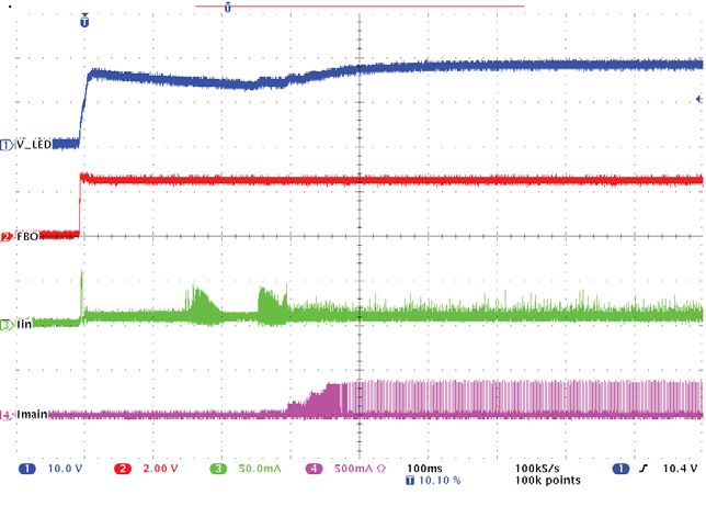
1. Introduction
The MSL2021 LED driver for two-color systems includes a linear current controller for the main string, typically for white
LEDs, and a second floating buck controller for a color-adjust LED string. Both the switching and linear controllers drive
external MOSFETs to provide flexibility over a wide range of power levels (LED currents and voltages).
The MSL2021 adaptively manages the voltage powering the main LED string. A proprietary and patent pending
efficiency optimizer (EO) algorithm controls the voltage output of both AC/DC and DC/DC, isolated or non-isolated
topology, including ultra-low bandwidth single-stage PFC flyback controller.
The MSL2021 features peak current control and individual string PWM dimming, with the two strings driven at a 180out
of phase. The main LED string’s current is ripple-free and has very high accuracy. The PWM dimming frequency for both
LEDs strings is 400Hz to give a predictable and wide dimming range. A thermistor connection allows automatic
compensation of luminous efficacy in a two-color LED fixture to maintain consistent color balance across temperature.
The MSL2021 operates from 9.5V to 15V input. The color-adjust string voltage regulation loop uses a constant off-time
control algorithm to achieve stable control with good transient behavior. For flexibility of design, off-time is set with an
external resistor. LED current in both the strings can be adjusted using internal 8-bit DACs.
The internal registers are I2C accessible. Integrated non-volatile EEPROM memory, also accessed through the I2C serial
interface, allows configuration at final test in case that the factory default settings need to be modified.
The MSL2021 is available in the space-saving 24-pin 4x4mm QFN package and operate over the extended -40°C to
105°C operating range.
2. Ordering Information
Ordering code Description Package(1)
MSL2021IN Two String LED Driver 4 x 4mm 24-pin QFN
Note: 1. Lead-Free, Halogen-Free, RoHS Compliant Package
3. Application Circuit
WHITE LED STRING COLOR LED STRING
BRIDGE
RECTIFIER
&
EMI NTC
FILTER THM
SINGLE FBO
AC MAINS STAGE D
PFC
FLYBACK MSL2021
CONTROLLER LINEAR G LED
LED S DRIVER
DRIVER DRV
VDD CS
PWM1
FLOATING
BUCK LED
VIN DRIVER
MCU
MSL2021 [DATASHEET] 2
42062A–LED–02/2013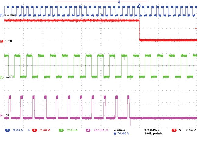
4.   Absolute Maximum Ratings
     Voltage with respect to AGND

               AVIN, PVIN, EN                                                              -0.3V to +16.5V

               VCC, PWM, FLTB, SDA, SCL, TOFF, REXT, FBO                                     -0.3V to +5.5V

               VDD                                                                         -0.3V to +2.75V

               THM                                                                     -0.3V to VCC+0.3V

               CS, S                                                                   -0.3V to VDD+0.3V

               D                                                                             -0.3V to +22V

               G, DRV                                                                   -0.3V to VIN+0.3V

               PGND, AGND                                                                    -0.3V to +0.3V

     Current (into pin)

               AVIN, PVIN, DRV, G (average)                                                             100mA

               PVIN (peak, =1% duty)                                                                       1A

               DRV, G (peak, =1% duty)                                                                    ±1A

               PGND (peak, =1% duty)                                                                       -1A

               AGND, PGND (average)                                                                 -100mA

               All other pins                                                                           ±10mA

     Continuous Power Dissipation at 70°C

               24-Pin 4mm x 4mm VQFN (derate 21.8mW/°C above TA = +70°C)                           1200mW

     Ambient Operating Temperature Range                                                  -40°C to +105°C

     Junction Temperature                                                                               +125°C

     Storage Temperature Range                                                            -65°C to +125°C

     Lead Soldering Temperature, 10s                                                                    +300°C

                                                                           MSL2021 [DATASHEET]               3
                                                                                   42062A–LED–02/2013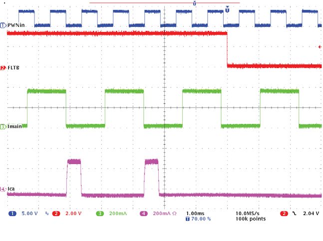
5. Electrical Characteristics
AVIN = PVIN = 12V, -40°C ≤TA ≤ 105°C, Typical Operating Circuit, unless otherwise noted.
Typical values at TA = +25°C.
Table 5-1. DC electrical characteristics
Parameter Conditions Min. Typ. Max. Unit
AVIN, PVIN Operating Supply Voltage 9.5 12 15 V
LEDs on at PWM = 100%,
AVIN Operating Supply Current 10 mA
serial interface idle
EN = SLEEP = 1,
AVIN Idle Supply Current 7 10 mA
all digital inputs = 0
EN = SLEEP = 1,
PVIN Idle Supply Current 0 μA
all digital inputs = 0
VEN = 0,
AVIN Disable Supply Current 5 μA
all digital inputs = 0
VCC Regulation Voltage IVCC = 10mA peak(7) 4.5 5 5.5 V
(7)
VDD Regulation Voltage IVDD = 10mA peak 2.25 2.5 2.75 V
PWM, PWM1, PWM2, SCL, SDA Input
0.7VVDD V
High Voltage
PWM, PWM1, PWM2, SCL, SDA Input
0.3VVDD V
Low Voltage
EN Input High Voltage 2 V
EN Input Low Voltage 0.5 V
EN Input Hysteresis 100 mV
SDA, FLTB Output Low Voltage Sinking 6mA 0.3 V
SCL, SDA, PWM, PWM1, PWM2, FLTB
-5 5 A
leakage current
S Current Sense Regulation Voltage TA = 25C, MREF = 0x64 194 200 206 mV
Main string at 100% duty
S Current Sense Regulation Voltage cycle, -3 +3 %
Accuracy
TA = 25C, MREF = 0x64
S Current Sense Regulation Voltage
-220 ppm/ºC
Temperature Coefficient
G Maximum Output Voltage AVIN – 3.5 9.5 AVIN – 2.0 V
D Regulation Threshold EOCTRL = 0xE5 0.9 1 1.1 V
CS Current Sense Regulation Voltage CAREF = 0x64 200 mV
VDRV = 12V, IDRV = 20mA 5.6 9 Ω
DRV Impedance
VDRV = 0V, IDRV = -20mA 5.6 9 Ω
FBO Full Scale Current 170 255 340 µA
MSL2021 [DATASHEET] 4
42062A–LED–02/2013
Parameter Conditions Min. Typ. Max. Unit
FBO LSB Current 1.0 A
THM Source Current 100 A
THM Voltage Range 0 1.5 V
Thermal Shutdown Temperature Temperature rising 133 °C
Thermal Shutdown Hysteresis 15 °C
Table 5-2. AC electrical characteristics
Parameter Conditions Min. Typ. Max. Unit
DRV tOFF timing RTOFF = 45.3k 0.5 s
(8)
PWM Input Frequency 60 10,000 Hz
PWM Duty Cycle 1 100 %
PWM Duty Cycle Resolution MSL2021 0.4 %
Table 5-3. I2C switching characteristics
Parameter Symbol Conditions Min. Typ. Max. Unit
(1)
SCL Clock Frequency 0.05 1,000 kHz
STOP to START Condition Bus Free
tBUF 0.5 µs
Time
Repeated START condition Hold Time tHD:STA 0.26 µs
Repeated START condition Setup Time tSU:STA 0.26 µs
STOP Condition Setup Time tSU:STOP 0.26 µs
SDA Data Hold Time tHD:DAT 5 ns
(2)
SDA Data Valid Acknowledge Time 0.05 0.55 µs
(3)
SDA Data Valid Time 0.05 0.55 µs
SDA Data Set-Up Time tSU:DAT 100 ns
SCL Clock Low Period tLOW 0.5 µs
SCL Clock High Period tHIGH 0.26 µs
(4)(5)
SDA, SCL Fall Time tF 120 ns
SDA, SCL Rise Time tR 120 ns
(6)
SDA, SCL Input Suppression Filter
50 ns
Period
(1)
Bus Timeout tTIMEOUT 25 ms
Notes: 1. Minimum SCL clock frequency is limited by the bus timeout feature, which resets the serial bus interface when either SDA or SCL is held low for tTIMEOUT.
2. SDA Data Valid Acknowledge Time is SCL LOW to SDA (out) LOW acknowledge time.
3. SDA Data Valid Time is minimum SDA output data-valid time following SCL LOW transition.
4. A master device must internally provide an SDA hold time of at least 300ns to ensure an SCL low state.
MSL2021 [DATASHEET] 5
42062A–LED–02/2013
5. The maximum SDA and SCL rise times is 300ns. The maximum SDA fall time is 250ns. This allows series protection resistors to be connected between SDA
and SCL inputs and the SDA/SCL bus lines without exceeding the maximum allowable rise time.
6. Includes input filters on SDA and SCL that suppress noise less than 50ns.
7. Additional decoupling may be required when pulling current from VCC and/or VDD in noisy environments.
8. 2µs minimum on time for main LED string PWM dimming.
Typical Operating Characteristics
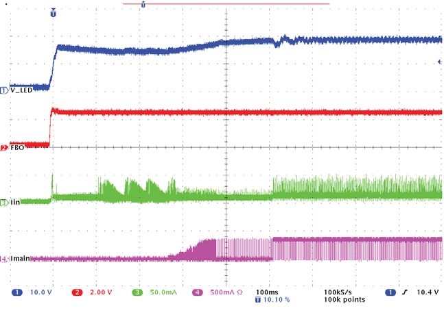
Figure 5-1. Start-up behavior, PWM = 10% duty cycle (Test conditions).
VLED
FBO
Iin
Imain
Figure 5-2. Start-up behavior, PWM = 90% duty cycle (Test conditions).
VLED
FBO
Iin
Imain
MSL2021 [DATASHEET] 6
42062A–LED–02/2013Figure 5-3. Normal operation, PWM = 10% duty cycle (Test conditions).
PWMin
Imain
Ica
Figure 5-4. Normal operation, PWM = 90% duty cycle (Test conditions).
PWMin
Imain
Ica
MSL2021 [DATASHEET] 7
42062A–LED–02/2013Figure 5-5. Fault response, string open circuit (Test conditions).
PWMin
FLTB
Imain
Ica
Figure 5-6. Fault response, LED short circuit (Test conditions).
PWMin
FLTB
Imain
Ica
MSL2021 [DATASHEET] 8
42062A–LED–02/2013Figure 5-7. Input current vs. input voltage
100
IIN
10
ISLEEP
1
IIN (mA)
f IN = 400Hz
0.1 PWM = 50%
0.01
ISHDN
0.001
0.0001
10 11 12 13 14 15
VIN (V)
Figure 5-8. Average LED current vs. input PWM duty cycle
100
f IN = 400Hz
MAIN STRING
80
LED CURRENT (%FS)
60
40
20
0
0 50 100
DUTY CYCLE (%)
MSL2021 [DATASHEET] 9
42062A–LED–02/2013Figure 5-9. VCC and VDD regulation
5.5
5.0
4.5 VCC
4.0
3.5
VOUT (V)
3.0
2.5
2.0 VDD
1.5
1.0 f IN = 400Hz
0.5 PWM = 50%
0.0
0 20 40 60 80 100
IOUT (mA)
MSL2021 [DATASHEET] 10
42062A–LED–02/20136. Block Diagram
Figure 6-1. MSL2021 block diagram
AVIN
D
VDD EFFICIENCY OPTIMIZER
REGULATORS
VCC
VREF
FBO
DAC
G
VREF
EN CONTROL LOGIC
S
FLTB START
CLOCK
FAULT
DETECT OSCILLATOR MUX
PWM PWM DIGITIZER 400HZ PWM
GENERATOR
SDCR REGISTER AND
DUTY CYCLE
LOOK-UP TABLE EEPROM ENGINE PVIN
THM ADC
DRV
CURRENT S Q
TOFF
GENERATOR
CS
R QB
CURRENT
GENERATOR
VREF
COFF
1.2V DAC
REXT
AGND PGND
MSL2021 [DATASHEET] 11
42062A–LED–02/20137. Pinout and Pin Description
7.1 Pinout MSL2021
AGND
AVIN
VDD
VCC
D
G
24 23 22 21 20 19
FBO 1 18 S
EN 2 17 NC
PWM 3 MSL2021 16 PVIN
SCL 4 (TOP VIEW) 15 DRV
SDA 5 14 PGND
FLTB 6 13 CS
7 8 9 10 11 12
NC
THM
REXT
TOFF
DNC
CGND
7.2 Pin Descriptions
Name Pin Description
Feedback Output
FBO 1 Feedback output from Efficiency Optimizer. Connect FBO to the LED power supply regulation
feedback node to control VLED. When unused connect FBO to VCC.
Enable Input (Active High)
EN 2 Drive EN high to turn on the MSL2021, drive EN low to turn it off. For automatic start-up connect EN to
AVIN.
PWM Dimming Input
PWM 3 Drive PWM with a pulse-width modulated signal to control LED brightness. See “PWM and LED
Brightness” on page 20 for details.
Serial Clock Input
SCL 4
SCL is the I²C serial interface clock input. See “I²C Serial Interface ” on page 31 details.
Serial Data Input/Output
SDA 5
SDA is the I²C serial interface data I/O. See “I²C Serial Interface ” on page 31 details.
Fault Output (Open Drain, Active Low)
FLTB sinks current to AGND when a fault condition exists. Toggle EN low then high to clear FLTB, or
FLTB 6
clear faults through the serial interface (see “Fault Status register (FAULTSTAT, 0x23), Read Only” on
page 29). Use the serial interface to access fault information and to enable/disable fault response.
MSL2021 [DATASHEET] 12
42062A–LED–02/2013Name Pin Description
NC 7, 17 No Internal Connection
NTC Thermistor Sensing Input
Connect a negative temperature coefficient thermistor (ERT-J0EG103FA or equivalent) from THM to
THM 8 AGND, in series with a 1.5kΩ resistor. Locate the thermistor close to the Color-Adjust LEDs to monitor
their temperature. This allows the MSL2021 to automatically temperature compensate the Color-
Adjust string brightness.
External Resistor
REXT 9
Connect a 46.4k, 1% resistor from REXT to AGND.
Off-Time Set Input
A resistor from TOFF to AGND controls the constant off time for the Color-Adjust string floating buck
TOFF 10
converter, where RTOFF = tOFF (90.9 x 10⁹), with tOFF in seconds and RTOFF in Ohms. For example, an
off time of 0.5s results in a resistor value of 45.3k (to the nearest 1% value).
Do Not Connect
DNC 11
Do not make external connection to DNC.
Connect to Ground
CGND 12
Connect CGND to AGND.
Current Sense Input for the Color-Adjust String
CS 13 Connect CS to the external current sense resistor of the Color-Adjust string. The current sense
threshold is 200mV.
Power Ground
PGND 14 PGND is the ground connection for the FET gate drivers. Connect PGND to AGND close to the
MSL2021.
Gate Drive for Color-Adjust (Floating Buck Regulator) MOSFET
DRV 15
Connect DRV to the gate of the external power MOSFET.
Power Voltage Input
PVIN 16 PVIN powers DRV, the floating buck FET gate driver. Bypass PVIN to PGND with a 1.0µF or greater
capacitor.
Source Sense Input for Main LED String MOSFET
S 18 Connect S to the source of the external MOSFET, and to the current sense resistor for the Main LED
string. The current sense threshold is 200mV.
Gate Output for Main String MOSFET
G 19
Connect G to the gate of the Main string external MOSFET.
Drain Output for Main String MOSFET
D 20
Connect D to the drain of the Main string external MOSFET.
Analog Voltage Input
AVIN 21 AVIN is the power input to the MSL2021. Bypass AVIN to AGND with a 1.0µF or greater capacitor
placed close to AVIN.
5V Internal Voltage
VCC 22
Connect 10uF bypass capacitor from VCC to AGND.
Analog Ground
AGND 23
Connect AGND to system ground.
2.5V Internal Voltage
VDD 24
Connect 10uF bypass capacitor from VDD to AGND.
Exposed Pad
EP EP EP is the Main thermal path for heat to escape the die. Connect EP to a large copper plane connected
to PGND and AGND.
MSL2021 [DATASHEET] 13
42062A–LED–02/20138. Typical Application Circuit
MSL2021 controlling the output of an isolated PFC controller; a linear current sink regulates the white LED string current
and a floating buck converter regulates the color LED string current.
Figure 8-1. Typical application circuit
VAC RTOP
AC-DC RBOTTOM
ISOLATED
With PFC
COLOR
LEDS
WHITE
LEDS
ERT-
100kΩ J0EG103FA
1μF
FBO D
EN EN
PWM PWM Q1
G
FAULT FLTB 820μH
S
1μF PVIN 0.56Ω
MSL2021 D1
+
LED DRIVER
12V 1μF AVIN
- 46.4kΩ THM
REXT 1.50kΩ Q2
TOFF DRV
VCC CS
10μF
VDD PGND 0.56Ω
AGND SDA SCL
45.3kΩ 10uF
CONFIGURATION INTERFACE
(OPTIONAL)
9. Detailed Description
The MSL2021 drives two LED strings, the main string and the color-adjust string. The main string LEDs are typically
white and used to provide accurate light intensity control.The color-adjust string LEDs are used to control the color
temperature. The combined light output is a blended high CRI light, for example, than what white LEDs can alone
produce. The main string is directly controlled by a Pulse Width Modulated (PWM) constant current controller (current
sink to ground). An Efficiency Optimizer (EO) output controls the main string voltage, via feed-back to the LED string
power supply, to minimize the voltage across the LED current controller, minimizing power loss.
The color-adjust string is regulated by a floating buck controller. The buck controller converts the voltage of the main
string’s supply to a voltage appropriate for the color-adjust LEDs. Additionally, the MSL2021 has a programmable 8-bit
registers that allows adjustment of the current by changing the source feedback reference voltages (see“Block Diagram”
on page 11).
MSL2021 [DATASHEET] 14
42062A–LED–02/201310. Fault Conditions
The MSL2021 detects fault conditions, and takes corrective action when faults are verified.
String open circuit and LED short circuit conditions of the color-adjust string are monitored. When one of these faults
occurs, FLTB pulls low to indicate a fault condition and the color-adjust LEDs turn off. Read Fault Status register 0x23 to
determine the fault type. Clear these faults by toggling EN low then high. Faults that persist re-establish the fault
response. Mask string faults using Fault Disable register 0x22.
For the main LED string, when an open LED occurs, the voltage of the AC/DC or DC/DC input power supply reaches the
maximum allowed.
Over-temperature protection puts the device to sleep when the die temperature is above 133C. The device turns back
on when the die temperature falls below 118C, and normal operation resumes. While asleep, the I2C interface remains
active; see “Fault Disable register (FAULT, 0x22)” and “Fault Status register (FAULTSTAT, 0x23), Read Only” on page
29 for more information about thermal shutdown.
Table 10-1. Fault Conditions, Response and Recovery
Fault Response Recovery action
When die temperature falls below 118C operation
Die Temperature > 133C Asleep (I2C still active)
resumes as if EN is pulled high
Color-adjust string turns off, FLTB pulls
Color-adjust string has Correct the short condition in LED string. Toggle EN low to
low, and bit 0 of the Fault Status register
shorted LEDs high to resume operation
0x23 sets high
Color-adjust string turns off, FLTB pulls
Color-adjust string is open Correct the open condition in LED string. Toggle EN low to
low, and bit 1 of the Fault Status register
circuit high resume operation
0x23 sets high
11. Applications Information
11.1 Turn-On Sequence
The MSL2021 waits for 250ms after power is applied to allow the AC/DC or DC/DC input supply to establish the default
voltage. Then the MSL2021 starts to optimize the LED string voltage (VLED), and then starts to drive the LED strings. It is
critical that the AC/DC or DC/DC converter that powers the LED strings reaches its nominal output voltage in less than
250ms after power is applied. When the 250ms start-up delay is complete, the efficiency optimizer adjusts the LED
voltage to the proper level to drive the main string. After the voltage is set, normal PWM operation begins for both the
main and color-adjust strings. This turn-on sequence allows the light to come up at the proper color and intensity without
flashing or flicker.
11.2 Setting the Main String Current with RS
The Main string LED on-current regulates by monitoring the voltage at the S pin, the main string MOSFET source resistor
connection. The default feedback voltage at the S pin is 200mV. Choose the string current sense resistor RS using:
0.2
R S = ------------
I LED
where ILED is the main string regulation current. The main string reference voltage (MREF) register 0x20 sets the
feedback voltage, to 200mV, at 2mV per LSB. The regulation voltage, VS(FB), is:
MSL2021 [DATASHEET] 15
42062A–LED–02/2013V S FB = 0.002 MREF V
where MREF is the decimal equivalent of the value in register 0x20. The default value for MREF is 0x64, for a feedback
voltage of 0.2V. Change the feedback voltage by changing the value in register 0x20 using the serial interface. LED
average current is within ±3% of the targeted value when a 1% resistor is used for RS.
11.3 Setting AC/DC Output Voltage
The efficiency optimizer output, FBO, connects to the AC/DC or DC/DC converter’s output voltage feedback node, and
pulls current from the node to force the converter’s output voltage up. The MSL2021 works with any input power
converter topology that uses a resistor divider to set its output voltage. Operation with a AC/DC PFC converter is
described below.
Select the two resistors that set the nominal AC/DC LED power supply’s output voltage by first determining the minimum
output voltage using:
V OUT MIN V fMIN N + 0.2V
where VfMIN is the minimum LED forward voltage for the Main string LEDs at the expected LED current, N is the number
of LEDs in the string, and 0.2V is the minimum overhead required for the current sense resistor and the FET. Then
determine the maximum output voltage using:
V OUT MAX = V fMAX N + 1.2V
where VfMAX is the maximum LED forward voltage for the Main string LEDs at the operating LED current, N is the number
of LEDs in the string, and 1.2V is the maximum overhead required for the current sense resistor and the FET. Determine
the value for the upper voltage setting resistor using:
V OUT MAX – V OUT MIN
R TOP -----------------------------------------------------------------
–6
170 10
where 170A is the minimum FBO full scale current. Determine the lower resistor using:
V FB
R BOTTOM = R TOP --------------------------------------------
V OUT MIN – V FB
where VFB is the feedback regulation voltage of the switch mode converter.
11.4 Selecting the Main String MOSFET
The Main string MOSFET sinks the string current to ground through current sense resistor RS. Output of pin G drives the
gate of the MOSFET at up to VIN - 2V. Select a MOSFET with a maximum drain-source voltage of at least 20% above:
R TOP
V fb ------------------------ + 1 + 340A R TOP
R
BOTTOM
where 340µA is the maximum FBO full scale current.
11.5 Selecting the Drain Resistor – RD
The drain resistor, RD, connects the MSL2021 to the drain of the main string external MOSFET. Use a 100k for RD.
MSL2021 [DATASHEET] 16
42062A–LED–02/201311.6 Selecting the Color-Adjust String Floating Buck Components
Figure 11-1. Floating buck LED driver
WHITE LEDS COLOR LEDS
(MAIN STRING) (COLOR-ADJUST STRING)
VLED
Ci +
IAVE
VBUCK
-
Co
Lo D1
MSL2021
LED Driver
Q
DRV
TOFF CS
RTOFF RCS
PGND
The MSL2021 includes a driver for a constant off-time floating buck topology, shown in Figure 11-1, to convert the main
string voltage to a value appropriate for the color-adjust LED string. The buck is operated in continuous conduction
mode.
Continuous conduction operation is assured when the peak-to-peak ripple current in the inductor, ∆iL, is less than twice
the average LED current. A peak-to-peak ripple current magnitude of 15% of the average LED on-current is suggested,
i.e.
i L 0.15I AVE A
where IAVE is the average color-adjust LED string on-current. Choose IAVE appropriate for the color-adjust LEDs (Figure
11-1 on page 17 and Figure 11-2 on page 18) and calculate the peak string on-current using
i
I PEAK = I AVE + -------L- A
2
MSL2021 [DATASHEET] 17
42062A–LED–02/2013Figure 11-2. Color-adjust string LED on-current details.
I
INDUCTOR CURRENT
IPEAK
IAVE ? iL
LED CURRENT
tOFF (WHEN USING CO)
t
The color-adjust string LED on-current regulates by monitoring the voltage at CS, the color-adjust string FET source
resistor connection. The reference voltage VCSFB for CS is 200mV (VCSFB is 200mV by default, and is adjustable through
the serial interface; see the register definitions for details about changing VCSFB). Choose the current sense resistor RCS
using
V CSFB
R CS = ----------------
I PEAK
Determine VBUCK, the voltage across the color-adjust LEDs, using
V BUCK = NV f V
where N is the number of LEDs in the string and VF is the forward voltage drop of the LEDs at IPEAK.
The duty ratio of MOSFET Q is
V BUCK
D = ----------------
-
V LED
where VLED is the main string voltage, Figure 11-1 on page 17. The constant off-time of the MOSFET is toff and calculated
in seconds using
t off = 1 – D-
------------ s
fs
where fS is the selected switching frequency in Hz. Use 100kHz to 1MHz for fS. Set toff with resistor RTOFF from TOFF to
GND (Figure 11-1 on page 17), whose value is
9
Rt = t off 90.9 10
off
Choose the inductor value using
V BUCK t off
-H
L O = -----------------------------
i L
Use a ferrite inductor with a saturation current at least 50% higher than the peak current flowing in it:
IL 1.5 I PEAK A
SAT
Note here a particular advantage of constant off-time operation of the buck converter is that ripple current is independent
of the input voltage. The circuit provides a constant average LED current, IAVE, but the buck converter actually regulates
the peak inductor current, IPEAK (Figure 11-1 on page 17 and Figure 11-2 on page 18). From the equation for the inductor
value L0 above, we see that because toff is constant, and VBUCK is relatively constant, the ripple current ∆iL is also
constant, so that IAVE is a constant, as desired. If the main string voltage changes, the switching frequency changes to
keep the on-time constant, thus the ripple current is independent of the input voltage.
MSL2021 [DATASHEET] 18
42062A–LED–02/2013This topology does not require an output capacitor, Co in Figure 11-1 on page 17. When used, Co steers the inductor’s
ripple current away from the LEDs but reduces the accuracy of PWM dimming because the voltage across it cannot
change quickly. When using Co, a ceramic capacitor of between 1.0µF and 10µF is adequate, with a voltage rating higher
than VBUCK.
The output capacitor of the AC/DC converter that produces the main string voltage, Ci in Figure 11-1 on page 17, doubles
as the buck’s input capacitor. The capacitor’s function is to provide a smooth voltage to the buck converter. It should be
able to handle the R.M.S. ripple current of the buck converter, which is approximately equal to
I C = I AVE D 1 – D A
i
This ripple current peaks at a duty ratio of D = 0.5.
Select an N-channel MOSFET for Q with a maximum drain-source voltage at least 25% above VLED. The R.M.S. current
in the MOSFET is approximately equal to
I Q = I AVE D A
The MOSFET conduction power loss due to this current is
PCON I Q2 RDS I AVE
2
RDS D
W
where RDS is the hot on-resistance of the MOSFET, which can be found in the MOSFET datasheet, and is typically 1.5 to
1.8 times greater than the cold resistance. The MOSFET will also incur switching losses, which can be difficult to
calculate exactly. A good rule-of-thumb is to choose a MOSFET in a package that dissipates at least four times PCON.
The average current in the output rectifier D1 is
I D = I AVE 1 – D A
i
and the power dissipated in the rectifier due to conduction is
P CON = I D V on W
D1 1
where Von is the voltage drop across the rectifier at the forward current of ID1. Pick a rectifier with an average current
rating at least 50% higher than ID1. Use a Schottky rectifier if the LED voltage is less than 50V. The Schottky rectifier’s
voltage rating should be at least 25% higher than VLED. Schottky rectifiers have very low on-state voltage and very fast
switching speed, but at high voltage and high temperatures their leakage current becomes significant. The power
dissipated in the Schottky rectifier due to the leakage current at any temperature and duty ratio is
P lkg = V LED I r D W
where Ir is the reverse leakage current, found in the diode’s datasheet. This power must be added to the conduction
power loss.
P D = P CON + P lkg W
1 D
Make sure that the rectifier’s total power dissipation is within the rectifier’s specifications.
MSL2021 [DATASHEET] 19
42062A–LED–02/201311.7 PWM and LED Brightness
The “Block Diagram” on page 11 shows how the MSL2021 controls the brightness of the LEDs. The duty cycle of the
main string equals the duty cycle of the input signal at PWM. The PWM input accepts an input signal frequency of 60Hz
to 10kHz, while the LED dimming frequency, of both the main and color-adjust strings, is 400Hz. The duty cycle of the
color-adjust string is based on the duty cycle of the signal at the PWM input, but compensated for temperature based on
a programmable look-up table, whose defaults are presented in Table 11-2 on page 21. See “Light Color and the THM
Input” on page 20 for temperature adjustment information.
Figure 11-3. LED current and duty cycle control.
MSL2021
RD
D
DAC + G
0x20 -
400Hz CLOCK EN S
RS
PWM
PWM ENGINE
DAC EN
THERMAL + DRV
THM 0x21
MONITOR -
CS
RCS
11.8 Light Color and the THM Input
The overall color of the light generated by the two LED strings is a blend of the main string’s white LEDs and the color-
adjust string’s color LEDs. Brightness is primarily controlled by the duty cycles of the PWM signals driving the LEDs. The
brightness of white LEDs is relatively constant over temperature, but the brightness of color LEDs may drop significantly
as temperature increases. The main string’s PWM duty cycle is fixed at the duty cycle of the input PWM signal, but the
duty cycle of the color-adjust string is changed as the LED temperature changes, to keep the blended light color
constant.
The thermistor input, THM, monitors the temperature of an external thermistor connected from THM to ground. A fixed
current is forced out THM to generate a voltage that is proportional to the thermistor’s temperature. The THM voltage is
measured by a 8-bit ADC internal to the MSL2021. When used with the suggested thermistor (ERT-J0EG103FA or
equivalent) in series with a 1.5kΩ resistor, THM measures temperatures from 18oC to 80oC with 2oC resolution, for 32
different temperature values. When the temperature is below 18oC, 18oC is returned by the temperature monitor circuit.
When the temperature is above 80oC, 80oC is returned by the temperature monitor circuit. The temperature information
is fed to the color-adjust string’s duty cycle circuit.
MSL2021 [DATASHEET] 20
42062A–LED–02/2013The MSL2021 modifies the color-adjust string duty cycle using a look-up table. Default values are presented in Table 11-
1; each location in the table corresponds to one temperature. The modification value is stored in the table as an 8-bit
color-adjust duty cycle ratio (SDCR). The SDCR, a number from 0 to 255, is divided by 255, and multiplied by the duty
cycle of the incoming PWM signal. The result is the duty cycle of the color-adjust string. The table is programmable
through the serial interface when values different from the defaults are desired.
Table 11-1. Temperature based duty cycle modification of the color-adjust string
COLOR-ADJUST DUTY CYCL
Part TEMPERATURE ADJUSTMENT Limits
SDCRxx = VALUE IN LOOK-UP TABLE 0x00 THRU 0x1F
SDCRxx
MSL2021 DC CA = ---------------------- DC PWM SDCRxx = 0xFF RETURNS 100% OF THE PWM DUTY CYCLE
255
SDCRxx = 0x00 RETURNS 0% OF THE PWM DUTY CYCLE
Table 11-2. Temperature Look-Up Table Defaults(1)
Register Multiplication factor
Temperature (°C) SDCRxx
----------------------
255
Address Name Default Value
≤18 0x00 SDCR18 0x4C 0.300
20 0x01 SDCR20 0x4D 0.303
22 0x02 SDCR22 0x4E 0.307
24 0x03 SDCR24 0x4F 0.311
26 0x04 SDCR26 0x50 0.314
28 0x05 SDCR28 0x51 0.318
30 0x06 SDCR30 0x52 0.322
32 0x07 SDCR32 0x53 0.327
34 0x08 SDCR34 0x54 0.331
36 0x09 SDCR36 0x55 0.336
38 0x0A SDCR38 0x56 0.340
40 0x0B SDCR40 0x58 0.345
42 0x0C SDCR42 0x59 0.350
44 0x0D SDCR44 0x5A 0.355
46 0x0E SDCR46 0x5C 0.361
48 0x0F SDCR48 0x5D 0.367
50 0x10 SDCR50 0x5E 0.373
52 0x11 SDCR52 0x60 0.379
54 0x12 SDCR54 0x62 0.385
56 0x13 SDCR56 0x63 0.392
58 0x14 SDCR58 0x65 0.399
MSL2021 [DATASHEET] 21
42062A–LED–02/2013Register Multiplication factor
Temperature (°C) SDCRxx
----------------------
255
Address Name Default Value
60 0x15 SDCR60 0x67 0.406
62 0x16 SDCR62 0x69 0.414
64 0x17 SDCR24 0x6B 0.422
66 0x18 SDCR66 0x6D 0.431
68 0x19 SDCR68 0x70 0.440
70 0x1A SDCR70 0x72 0.450
72 0x1B SDCR72 0x72 0.460
74 0x1C SDCR74 0x72 0.460
76 0x1D SDCR76 0x72 0.460
78 0x1E SDCR78 0x72 0.460
≥80 0x1F SDCR70 0x72 0.460
Note: 1. Change SDCRxx values through the serial interface
Figure 11-4. MSL2021 default look-up Table color correction vs. temperature.
1
DUTY CYCLE MULTIPLICATION FACTOR
0.9
0.8
0.7
0.6
0.5
0.4
0.3
0.2
0.1
0
0 20 40 60 80 100
TEMPERATURE (ºC)
MSL2021 [DATASHEET] 22
42062A–LED–02/201311.9 MSL2021 Look-Up Table Lockout Procedure
The MSL2021 features a lock for the look-up table. When locked, the table’s registers (0x00 through 0x1F) become read-
only. A locked table cannot be unlocked; changing the table’s registers is no longer possible. Reads of a locked table’s
registers return 0x00, unless the password (chosen when locking the table) is first entered to make the registers visible.
Locking the table requires use of the I2C interface to enter data, read data and program the EEPROM. For information
about using the I2C interface, see “I²C Serial Interface ” on page 31. For information about programming the EEPROM
see “EEPROM Address and Control/Status Registers” on page 26.
Lock the table by performing the following sequence; an example is presented below:
1. Fill the look-up table with data.
2. Commit the look-up table to EEPROM.
3. Cycle power, then verify the contents of the look-up table.
4. Choose a 16-bit password.
5. Enter the password into Password Registers 0x68 and 0x69.
6. Enter the password into Password Verification Registers 0x38 and 0x39.
7. Commit the password to EEPROM.
8. Set the lock bit.
9. Commit the lock bit to EEPROM.
10. Cycle power to the MSL2021.
11.9.1 Example:
The Look-Up Table is four pages long (each page is 8-bytes). When the look-up table is filled with the proper data,
commit the data to the EEPROM, one page at a time, by sending the following commands to the MSL2021 through its
I2C interface:
0x60 0x00 {to register 0x60 write 0x00: sets the EEPROM write pointer to 0x00}
0x61 0x04 {to register 0x61 write 0x04: writes the first page (8 bytes) of data to the EEPROM}
Wait 5ms.
0x61 0x00 {to register 0x61 write 0x00 : disables EEPROM writing}
0x60 0x08 {sets the EEPROM write pointer to 0x08}
0x61 0x04 {writes the second page of data to the EEPROM}
Wait 5ms.
0x61 0x00 {disables EEPROM writing}
0x60 0x10 {sets the EEPROM write pointer to 0x10}
0x61 0x04 {writes the third page of data to the EEPROM}
Wait 5ms.
0x61 0x00 {disables EEPROM writing}
0x60 0x18 {sets the EEPROM write pointer to 0x18}
0x61 0x04 {writes the final page of data to the EEPROM}
Wait 5ms.
MSL2021 [DATASHEET] 23
42062A–LED–02/20130x61 0x00 {disables EEPROM writing}
The EEPROM is now programmed with the data that are in registers 0x00 through 0x1F (the look-up table). Although not
required, now is a good time to cycle power to the MSL2021, then read registers 0x00 through 0x1F to verify that the
EEPROM was properly programmed (at power-up the EEPROM automatically programs registers 0x00 through 0x40).
Next, choose a 16-bit password and write it into the Password Registers, and into the Password Verification Registers.
For this example the password is 0xAA55:
0x68 0xAA
0x69 0x55 {writes the password into the password registers 0x68 and 0x69}
0x38 0xAA
0x38 0x55 {writes the same password into the password verification registers 0x38 and 0x39}
Now commit the password to EEPROM.
0x60 0x68 {sets the EEPROM write pointer to 0x68}
0x61 0x03 {writes the first byte of the password to the EEPROM}
Wait 5ms.
0x61 0x00 {disables EEPROM writing}
0x60 0x69 {sets the EEPROM write pointer to 0x69}
0x61 0x03 {writes the second byte of the password to the EEPROM}
Wait 5ms.
0x61 0x00 {disables EEPROM writing}
Next, set the lock bit and commit it to EEPROM.
0x3A 0x02 {sets the lock bit (bit D1) in register 0x3A}
0x60 0x3A {sets the EEPROM write pointer to 0x3A}
0x61 0x03 {writes the contents of register 0x3A to the EEPROM}
Wait 5ms.
0x61 0x00 {disables EEPROM writing}
Now cycle power to the MSL2021. All reads of the Look-Up Table now return 0x00.
To read the Table, enter the password into the password verification registers:
0x38 0xAA
0x39 0x55 {writes the password into registers 0x38 and 0x39}
MSL2021 [DATASHEET] 24
42062A–LED–02/2013Reads of the Look-Up Table now return its true contents, until the password register is changed, power is cycled or
enable input EN is toggled.
12. Control Registers
Table 12-1. Register map(1)
Bit functions
Address and Default
Function
Register name value(2)
D7 D6 D5 D4 D3 D2 D1 D0
0x00 SDCR18 Look up for 18C 0x4C Look up table
0x01 SDCR20 Look up for 20C 0x4D Look up table
…thru… …thru…
0x1E SDCR78 Look up for 78C 0x72 Look up table
0x1F SDCR80 Look up for 80C 0x72 Look up table
Main String
Feedback
0x20 MREF 0x64 MSREF = 2mV per LSB
Reference
Voltage
Color-Adjust
0x21 CAREF String Reference 0x64 VCAREF = 2mV per LSB
Feedback Voltage
FAULT Color-Adjust Fault
0x22 0x00 - - - - - TSDMASK OCDIS SCDIS
DISABLE Disable
Read
0x23 FAULTSTAT Fault Status - - - - - TSD OCFLT SCFLT
Only
0x24 SLEEP Configuration 0x00 - - - - - - - SLEEP
Read
0x31 TEMP Temperature Thermistor temperature
Only
Look-Up Table
Password
0x38 PWV(HIGH) 0xFF Look-Up Table Password Verification [15:8]
Verification High
Byte
Look-Up Table
Password
0x39 PWV(LOW) 0xFF Look-Up Table Password Verification [7:0]
Verification Low
Byte
Look-Up Table
0x3A LUT LOCK 0x83 - - - - - - LOCK[1:0]
Lock
Efficiency
0x40 EOCTRL 0xE5 - - - - DThresh[3:0]
Optimizer
EEPROM
0x60 E2ADDR 0x00 - EEPROM Address Pointer
Address
0x61 E2CTRL EEPROM Control 0x00 - - - - - RWCTRL[2:0]
Look-Up Table
0x68 PW(HIGH) Password High 0xFF Look-Up Table Password [15:8]
Byte
Look-Up Table
0x69 PW(LOW) Password Low 0xFF Look-Up Table Password [7:0]
Byte
Notes: 1. Do not change the contents of undefined bits or unlisted registers.
2. Unless changed through the EEPROM, these default values load at power-up, and when EN is taken from low to high.
MSL2021 [DATASHEET] 25
42062A–LED–02/201312.1 EEPROM and Power-Up Defaults
An on-chip EEPROM holds all the default register values. At power-up the data in the EEPROM is transferred directly to
control registers 0x00 thru 0x51, setting up the device for operation.
Any changes made to registers 0x00 thru 0x69 after power-up are not reflected in the EEPROM and are lost when power
is removed from the device, or when the enable input EN is forced low. If a different power-up condition is desired
program the values into the EEPROM via the serial interface as explained in the next section, or contact the factory to
inquire about ordering a customized power-up setting.
12.2 EEPROM Address and Control/Status Registers
The EEPROM can be visualized as an image of the control registers from 0x00 thru 0x69. Change an EEPROM register
value by writing the new value into the associated control register, and then instructing the device to program that value
into the EEPROM. Two control registers facilitate this process, the EEPROM address register E2ADDR (0x60), and the
EEPROM control register E2CTRL (0x61). Into E2ADDR write the location of the data that is to be programmed into the
EEPROM, and write 0x03 to E2CTRL to command the device to program that data into the EEPROM. Programming the
EEPROM takes a finite amount of time; after sending a command to E2CTRL wait 5ms, then end the write cycle by
writing 0x00 to E2CTRL.
Example: Change the string current feedback voltage MREF to 100mV.
Commands: To register 0x20 (MREF) write 0x32 (the new value for MREF). To register 0x60 (E2ADDR) write 0x20 (the
address of the MREF register). To register 0x61 (E2CTRL) write 0x03 (the command to copy the value to EEPROM).
Wait 5ms. To register 0x61 (E2CTRL) write 0x00, to turn off EEPROM access.
Result: The value 0x32, located in the MREF register, is programmed into the EEPROM and becomes the new power-
up default value for MREF.
Summary:
0x20 32
0x60 20
0x61 03
Wait 5ms
0x61 00
E2CTRL provides additional functions beyond simply programming a register’s value into the EEPROM. Data may be
transferred in either direction, from the registers to the EEPROM, or from the EEPROM to the registers. Register data
may be transferred into or out of the EEPROM in groups of eight, a page at a time. The page address boundaries are
predefined, and E2ADDR must be loaded with the address of the first byte of the page that is to be copied. Page
addresses begin at 0x00 and increment by eight, with the second page beginning at 0x08, the third at 0x10, etc. To
program a full page of data into the EEPROM, write the address of the page’s first byte to E2ADDR, and write 0x04 to
E2CTRL. Wait 5ms, and then end the write cycle by writing 0x00 to E2CTRL. When finished accessing the EEPROM
always write 0x00 to E2CTRL to block inadvertent EEPROM read/writes. Table 12-2 on page 26 details the functions
available through E2CTRL.
Table 12-2. EEPROM Address Register (E2ADDR, 0x60), defaults highlighted.
Register data
Register Address
D7 D6 D5 D4 D3 D2 D1 D0
E2ADDR 0x60 - E2ADDR[6:0]
DEFAULT 0 0 0 0 0 0 0 0
EEPROM Minimum Address 0x00 - 0 0 0 0 0 0 0
EEPROM Maximum Address 0x51 - 1 0 1 0 0 0 1
MSL2021 [DATASHEET] 26
42062A–LED–02/2013Table 12-3. EEPROM Status Register (E2CTRL, 0x61), defaults highlighted.
Register data
Register Address
D7 D6 D5 D4 D3 D2 D1 D0
E2CTRL 0x61 - - - - - RWCTRL[2:0]
DEFAULT 0 0 0 0 0 0 0 0
EEPROM Read / Write Disabled x x x x x 0 0 0
Read 1 Byte from EEPROM x x x x x 0 0 1
Read 8 Bytes from EEPROM x x x x x 0 1 0
Write 1 Byte to EEPROM x x x x x 0 1 1
Write 8 Bytes to EEPROM x x x x x 1 0 0
x x x x x 1 0 1
Unused
x x x x x 1 1 x
13. Detailed Register Descriptions
The MSL2021 registers are summarized in “Control Registers” on page 25. Detailed register information follows.
13.1 String Duty Cycle Control Registers (SDCR18 through SDCR80, 0x00 through 0x1F)
Holds the look-up table for the thermistor color-adjust string duty cycle correction. See “Light Color and the THM Input”
on page 20 for information. Put the device to sleep using SLEEP register 0x24 before modifying the SDCR values to
avoid undesired changes in the light output of the LEDs.
Table 13-1. String Duty Cycle Control Registers (SDCR18 through SDCR80, 0x00 through 0x1F), defaults highlighted
Register data
Register name Address
D7 D6 D5 D4 D3 D2 D1 D0
SDCR18 through SDCR80 0x00 – 0x1F SDCR[7:0]
DEFAULT (See Table 11-2 on page 21) X X X X X X X X
Correction factor = 0 0 0 0 0 0 0 0 0
Correction factor = 1 1 1 1 1 1 1 1 1
13.2 Main String Reference Voltage register (MREF, 0x20)
Holds the DAC value that controls the reference voltage for the main string FET source feedback voltage. The reference
voltage equals decimal value of this register times 2mV. The default value for MSREF is 0x64, which equates to MSREF =
200mV.
MSL2021 [DATASHEET] 27
42062A–LED–02/2013Table 13-2. Main String Reference register (MREF, 0x20), defaults highlighted
Register data
Register name Address
D7 D6 D5 D4 D3 D2 D1 D0
MREF 0x20 MREF[7:0]
DEFAULT: MREF = 100 * 2mV = 200mV 0 1 1 0 0 1 0 0
MREF = 0 2mV = 0V 0 0 0 0 0 0 0 0
MREF = 255 * 2mV = 510mV 1 1 1 1 1 1 1 1
13.3 Color-Adjust String Reference Voltage register (CAREF, 0x21)
Holds the DAC value that controls the reference voltage for the color-adjust string FET source feedback voltage. The
reference voltage equals decimal value of this register times 2mV. The default value for CASREF is 0x64, which equates
to CAREF = 200mV.
Table 13-3. Color-Adjust String Reference register (CAREF, 0x21), defaults highlighted
Register data
Register name Address
D7 D6 D5 D4 D3 D2 D1 D0
CAREF 0x21 CAREF[7:0]
DEFAULT: VCAREF = 100 * 2mV = 200mV 0 1 1 0 0 1 0 0
VCAREF = 0 2mV = 0mV 0 0 0 0 0 0 0 0
VCAREF = 255 2mV = 510mV 1 1 1 1 1 1 1 1
13.4 Fault Disable register (FAULT, 0x22)
Bits D0 and D1 control the fault response for the color-adjust string. For fault response behavior see “Fault Conditions”
on page 15. Bit D2 prevents the thermal shutdown fault from pulling FLTB low. Write 0x03 to this register to clear faults;
write 0x00 to re-enable fault response.
Table 13-4. Fault Disable register (FAULT, 0x22), defaults highlighted
Register data
Register name Address
D7 D6 D5 D4 D3 D2 D1 D0
FAULT 0x22 - - - - - TSDMASK OCDIS SCDIS
DEFAULT 0 0 0 0 0 0 1 1
Act on faults x x x x x 0 0 0
Disable LED Short Circuit Fault x x x x x x x 1
Disable String Open Circuit Fault x x x x x x 1 x
Do Not Allow Thermal Shutdown Fault to
x x x x x 1 x x
Pull FLTB Low
MSL2021 [DATASHEET] 28
42062A–LED–02/201313.5 Fault Status register (FAULTSTAT, 0x23), Read Only
Reports the fault status for the color-adjust string. When a fault is reported in this register, the fault output FLTB pulls low.
Toggle EN low, then high to clear the faults. Faults recur if the fault persists.
Table 13-5. Fault Status register (FAULTSTAT, 0x23), defaults highlighted
Register data
Register name Address
D7 D6 D5 D4 D3 D2 D1 D0
FAULTSTAT 0x23 - - - - - TSD OCFLT SSFLT
No Faults Detected x x x x x x 0 0
LED Short Circuit Fault Detected x x x x x x x 1
String Open Circuit Fault Detected x x x x x x 1 x
The MSL2021 is in Thermal Shutdown x x x x x 1 x x
13.6 Sleep register (SLEEP, 0x24)
Puts the device to sleep (the serial interface remains awake). When asleep, device supply current reduces to 7mA
(typical), the gate drive outputs stop switching, and the LEDs turn off.
Table 13-6. Sleep register (SLEEP, 0x24), defaults highlighted
Register data
Register name Address
D7 D6 D5 D4 D3 D2 D1 D0
SLEEP 0x24 - - - - - - - SLEEP
DEFAULT 0 0 0 0 0 0 0 0
Device is Awake x x x x x x x 0
Device is Asleep x x x x x x x 1
13.7 Thermistor Temperature register (TEMP, 0x31), Read Only
Reports the thermistor temperature at 2C per LSB. When the thermistor temperature is equal to or below 18C, this
register returns 0x12, or 18C. When the thermistor temperature is equal to or above 80C, this register returns 0x50, or
80C.
Table 13-7. Thermistor Temperature register (TEMP, 0x31), defaults highlighted
Register name
Register name Address
D7 D6 D5 D4 D3 D2 D1 D0
TEMP 0x31 TEMP[7:0]
Minimum Value: 0x12 = 18C 0 0 0 1 0 0 1 0
Maximum Value: 0x50 = 80C 0 1 0 1 0 0 0 0
MSL2021 [DATASHEET] 29
42062A–LED–02/201313.8 Password Verification registers
(PWV(HIGH) and PWV(LOW), 0x38 and 0x39)
Use these registers when locking the look-up table of the MSL2021. Also, enter the password (chosen when the Look-Up
Table was locked) into these registers to allow reading the contents of a locked look-up table. See section “MSL2021
Look-Up Table Lockout Procedure” on page 23 for details about locking the look-up table.
Table 13-8. Password Verification registers
(PWV(HIGH and PWV(LOW), 0x38 and 0x39), defaults highlighted
Register name
Register name Address
D7 D6 D5 D4 D3 D2 D1 D0
PWV(HIGH) 0x38 Password Verification High Byte [15:8]
PWV(LOW) 0x39 Password Verification Low Byte [7:0]
DEFAULT 1 1 1 1 1 1 1 1
13.9 Look-Up Table Lock register (LUT LOCK, 0x3A)
Use this register to lock the look-up table of the MSL2021. See section “MSL2021 Look-Up Table Lockout Procedure” on
page 23 for details about locking the look-up table. At power-up, this register returns 0x02 when the look-up table is
locked, and returns 0x83 when the table is unlocked.
Table 13-9. Look-Up Table Lock register (LUT LOCK, 0x3A), defaults highlighted
Register data
Register name Address
D7 D6 D5 D4 D3 D2 D1 D0
LUT LOCK 0x3A - - - - - - LOCK
DEFAULT 1 0 0 0 0 0 1 1
Locks the Look-Up Table when committed to
0 0 0 0 0 0 1 0
EEPROM
13.10 Efficiency Optimizer Control Register (EOCTRL, 0x40)
Configures voltage feedback threshold for D. It is recommended that SLEEP = 1 (bit D0 in the configuration register
0x24) while changing this register to avoid perturbations of the string power supply. The MSL2021 always performs a
power supply voltage calibration when power is applied, EN is taken high, or SLEEP is reset to 0. Do not change bits D4
through D7.
DThresh sets the voltage feedback threshold for D, The Main string FET drain connection.
D Threshold = (DThresh 150mV) + 250mV.
Table 13-10. Efficiency Optimizer Control Register (FBOCTRL, 0x40), default highlighted
Address / Register data
Register name
Default
D7 D6 D5 D4 D3 D2 D1 D0
FBOCTRL 0x40 - - - - DThresh[3:0]
DEFAULT = 0xE5 1 1 1 0 0 1 0 1
D Threshold = (0 150mV) + 250mV = 0.25V 1 1 1 0 0 0 0 0
MSL2021 [DATASHEET] 30
42062A–LED–02/2013Address / Register data
Register name
Default
D7 D6 D5 D4 D3 D2 D1 D0
••• •••
D Threshold = (5 150mV) + 250mV = 1V 1 1 1 0 0 1 0 1
••• •••
D Threshold = (15 150mV) + 250mV = 2.5V x 1 1 0 1 0 1 1
13.11 Registers 0x60 and 0x61, EEPROM Access
These registers control access to the EEPROM. See “EEPROM and Power-Up Defaults” and “EEPROM Address and
Control/Status Registers” on page 26 for information.
13.12 Password registers (PW(HIGH) and PW(LOW), 0x68 and 0x69)
Use these registers to enter the password when locking the look-up table of the MSL2021. See section “MSL2021 Look-
Up Table Lockout Procedure” on page 23 for details about locking the look-up table.
Table 13-11. Password registers
(PW(HIGH) and PW(LOW), 0x68 and 0x69), defaults highlighted
Register data
Register name Address
D7 D6 D5 D4 D3 D2 D1 D0
PWV(HIGH) 0x68 Password High Byte [15:8]
PWV(LOW) 0x69 Password Low Byte [7:0]
DEFAULT 1 1 1 1 1 1 1 1
14. I²C Serial Interface
The MSL2021 operates as a slave that sends and receives data through an I²C/SMBus compatible 2-wire serial
interface. The interface is not needed for operation, but is provided to allow control and monitoring of device functions.
These functions include changing the Look-Up Table and equation parameters, changing the string current reference
feedback voltages, reading and adjusting the fault response behavior and status, putting the device to sleep without
losing the register settings, and programming the EEPROM. The I²C/SMBus compatible interface is suitable for 100kHz,
400kHz and 1MHz communication. The interface uses data I/O SDA and clock input SCL to achieve bidirectional
communication between master and slaves. Fault output FLTB optionally alerts the host system to faults detected by the
MSL2021 (Figure 14-1 on page 32 and “Fault Conditions” on page 15). During over temperature shutdown (TSD) the
serial interface remains active.
The master, typically a microcontroller, initiates all data transfers, and generates the clock that synchronizes the
transfers. SDA operates as both an input and an open-drain output. SCL operates only as an input, and does not perform
clock-stretching. Pull-up resistors are required on SDA, SCL and FLTB.
MSL2021 [DATASHEET] 31
42062A–LED–02/2013Figure 14-1. I2C Interface Connections
VI2C
2 x 2.2k
TYPICAL 100k
MASTER SDA SDA
SCL SCL
(µC) INT FLTB MSL2021
A transmission consists of a START condition sent by a master, a 7-bit slave address plus one R/W bit, an acknowledge
bit, none or many data bytes each separated by an acknowledge bit, and a STOP condition (Figure 14-2, Figure 14-4 and
Figure 14-5 on page 33).
Figure 14-2. I2C Serial Interface Timing Details
SDA
tBUF
tSU:DAT tSU:STA
tHD:STA
tHD:DAT tSU:STO
tLOW
SCL
tHIGH
tHD:STA
tR tF
START REPEATED START STOP START
CONDITION CONDITION CONDITION CONDITION
14.1 I2C Bus Timeout
The bus timeout feature allows the MSL2021 to reset the serial bus interface if a communication ceases before a STOP
condition is sent. If SCL or SDA is low for more than 25ms (typical), then the MSL2021 terminates the transaction,
releases SDA and waits for another START condition.
14.2 I2C Bit Transfer
One data bit is transferred during each clock pulse. SDA must remain stable while SCL is high.
Figure 14-3. I2C Bit Transfer
SDA
SCL SDA LEVEL STABLE SDA ALLOWED TO
SDA DATA VALID CHANGE LEVEL
MSL2021 [DATASHEET] 32
42062A–LED–02/201314.3 I2C START and STOP Conditions
Both SCL and SDA remain high when the interface is free. The master signals a transmission with a START condition (S)
by transitioning SDA from high to low while SCL is high. When the master has finished communicating with the slave, it
issues a STOP condition (P) by transitioning SDA from low to high while SCL is high. The bus is then free.
Figure 14-4. I2C START and STOP Conditions
SDA
S P
SCL
START STOP
CONDITION CONDITION
14.4 I2C Acknowledge Bit
The acknowledge bit is a clocked 9th bit which the recipient uses to handshake receipt of each byte of data. The master
generates the 9th clock pulse, and the recipient holds SDA low during the high period of the clock pulse. When the
master is transmitting to the MSL2021, the MSL2021 pulls SDA low because the MSL2021 is the recipient. When the
MSL2021 is transmitting to the master, the master pulls SDA low because the master is the recipient.
Figure 14-5. I2C Acknowledge
SCL 1 2 8 9 1
SDA
TRANSMITTER
S A
SDA
RECEIVER
START ACKNOWLEDGE
CONDITION BY RECEIVER
14.5 I2C Slave Address
The MSL2021 has a 7-bit long slave address, 0b0100000, followed by an eighth bit, the R/W bit. The R/W bit is low for a
write to the MSL2021, high for a read from the MSL2021. All MSL2021 devices have the same slave address; when
using multiple devices and communicating with them through their serial interfaces, make external provision to route the
serial interface to the appropriate device. Note that development systems that use I2C often left-shift the address one
position before they insert the R/W bit, and so expect a default address of 0x20 (not 0x40).
MSL2021 [DATASHEET] 33
42062A–LED–02/2013Figure 14-6. I2C Slave Address
SDA A7 = 0 A6 = 1 A5 = 0 A4 = 0 A3 =0 A2 = 0 A1 = 0 R/W A
MSB
SCL 1 2 3 4 5 6 7 8 9
14.6 I2C Message Format for Writing to the MSL2021
A write to the MSL2021 contains the MSL2021’s slave address, the R/W bit cleared to 0, and at least 1 byte of
information (Figure 14-7 on page 34). The first byte of information is the register address byte. The register address byte
is stored as a register pointer, and determines which register the following byte is written into. If a STOP condition is
detected after the register address byte is received, then the MSL2021 takes no further action beyond setting the register
pointer.
Figure 14-7. I2C Writing a Register Pointer
ACKNO W LED GE ACKNO W LEDG E
START STO P
FRO M M SL202x FRO M M SL202x
SD A 0 1 0 0 0 0 0 0 A D7 . . . . . . D0 A
SLAVE AD DR ESS , SET REG ISTER
W R ITE AC CESS PO IN TER TO X
TH E R EG ISTER PO IN TER N OW POINTS TO X ; A SUBSEQ UEN T READ
ACCESS R EAD S FRO M R EG ISTER ADD RESS X
When no STOP condition is detected, the byte transmitted after the register address byte is a data byte, and is placed
into the register pointed to by the register address byte (Figure 14-8). To simplify writing to multiple consecutive registers,
the register pointer auto-increments during each following acknowledge period. Further data bytes transmitted before a
STOP condition fill subsequent registers.
Figure 14-8. I2C Writing Two Data Bytes
ACKNOWLEDGE ACKNOWLEDGE ACKNOWLEDGE ACKNOWLEDGE
START STOP
FROM MSL202x FROM MSL202x FROM MSL202x FROM MSL202x
SDA 0 1 0 0 0 0 0 0 A D7 . . . . . . D0 A D7 . . . . . . D0 A D7 . . . . . . D0 A
SLAVE ADDRESS, SET REGISTER DATA WRITES TO DATA WRITES TO
WRITE ACCESS POINTER TO X REGISTER X REGISTER X + 1
THE REGISTER POINTER NOW POINTS TO X + 2; A SUBSEQUENT READ
ACCESS BEGINS READING FROM REGISTER ADDRESS X + 2
14.7 I2C Message Format for Reading from the MSL2021
Read the MSL2021 registers using one of two techniques.
The first technique begins the same way as a write, by setting the register address pointer as shown in Figure 14-7,
including the STOP condition (note that even though the final objective is to read data, the R/W bit is first sent as a write
because the address pointer byte is being written into the device). Follow the Figure 14-7 transaction by what shown in
Figure 14-9, with a new START condition and the slave address, this time with the R/W bit set to 1 to indicate a read.
Then, after the slave initiated acknowledge bit, clock out as many bytes as desired, separated by master initiated
MSL2021 [DATASHEET] 34
42062A–LED–02/2013acknowledges. The pointer auto-increments during each master initiated acknowledge period. End the transmission with
a not-acknowledge followed by a stop condition.
Figure 14-9. I2C Reading Register Data with Preset Register Pointer
ACKNOWLEDGE ACKNOWLEDGE NOT ACKNOWLEDGE
START STOP
FROM MSL202x FROM MASTER FROM MASTER
SDA 0 1 0 0 0 0 0 1 A D7 . . . . . . D0 A D7 . . . . . . D0 A
SLAVE ADDRESS, READ REGISTER READ REGISTER
READ ACCESS ADDRESS X ADDRESS X + 1
THE REGISTER POINTER NOW POINTS TO X + 2; A SUBSEQUENT
READ ACCESS READS FROM REGISTER ADDRESS X + 2
The second read technique is illustrated in Figure 14-10. Write to the MSL2021 to set the register pointer, send a
repeated START condition after the second acknowledge bit, then send the slave address again with the R/W bit set to 1
to indicate a read. Then clock out the data bytes separated by master initiated acknowledge bits. The register pointer
auto-increments during each master initiated acknowledge period. End the transmission with a not-acknowledge
followed by a stop condition. This technique is recommended for buses with multiple masters, because the read
sequence is performed in one uninterruptible transaction.
Figure 14-10. I2C Reading Register Data Using a Repeated START
ACKNOWLEDGE ACKNOWLEDGE REPEATED ACKNOWLEDGE NOT ACKNOWLEDGE
START STOP
FROM MSL202x FROM MSL202x START FROM MSL202x FROM MASTER
SDA 0 1 0 0 0 0 0 0 A D7 . . . . . . D0 A 1 0 1 0 0 0 0 1 A D7 . . . . . . D0 A
SLAVE ADDRESS SET REGISTER SLAVE ADDRESS
READ REGISTERS
WRITE ACCESS POINTER READ ACCESS
14.8 I2C Message Format for Broadcast Writing to Multiple devices
With a broadcast write to MSL2021, a master broadcasts the same register data to all MSL2021s on the bus. First send
the broadcast write slave address of 0x00, followed by the MSL2021 broadcast device ID of 0x42. These two bytes are
followed by the register address in the MSL2021s that the following data are to be written into, and finally the data byte(s)
to be written into all devices.
A broadcast write example is shown in Figure 14-11. Here, the same register address in every MSL2021 is written to with
identical data. If further data bytes are transmitted before the STOP condition, they are stored in subsequent internal
registers of each MSL2021.
MSL2021 [DATASHEET] 35
42062A–LED–02/2013You can also read