ACTIVE DAMPING OF LCL FILTER RESONANCE IN GRID CONNECTED APPLICATIONS - Master Thesis
←
→
Page content transcription
If your browser does not render page correctly, please read the page content below
ACTIVE DAMPING OF LCL FILTER
RESONANCE IN GRID CONNECTED
                   APPLICATIONS

                                                                            Page 1 of 1

            Master Thesis
                  by
            Anca JULEAN
   PED10-1035 - Spring Semester, 2009

     http://cse-distributors.co.uk/danfoss-drives/micro-drive-diagram.jpg   29.09.2008
ii

Title:              Active damping of LCL filter resonance in grid connected applications

      Semester:           4th
      Semester theme:     Master Thesis
      Project period:     02.02.09 to 03.06.09
      ECTS:               30
      Supervisors:        Mihai CIOBOTARU
                          Lucian ASIMINOAEI
      Project group:      PED4 - 1035

                                                 SYNOPSIS:

                                                        The increasing development of re-
                                                 newable energy systems challenges more
                                                 and more the parameters of their connec-
                                                 tion to grid. The connection through an
  Anca Maria Julean                              LCL filter offers certain advantages, but it
                                                 brings also the disadvantage of having a
                                                 resonance frequency.
      Copies:     4                                     This project deals with the in-
    Pages, total: 83                             vestigation and the implementation of
     Appendix:    2                              different methods of active damping of
   Supplements: 3 CDs                            the LCL filter resonance in grid connected
                                                 applications.
                                                       In this project, different active damp-
                                                 ing methods are be reviewed. The control
                                                 of the inverter is be implemented, in-
                                                 cluding the synchronization with the grid,
                                                 the current and dc voltage control loop.
                                                 Also, different active damping methods
                                                 are implemented and tested under different
                                                 conditions.

By signing this document, each member of the group confirms that all participated
in the project work and thereby all members are collectively liable for the content of
the report.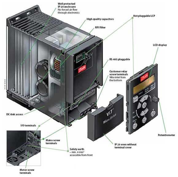
ii
Preface

The present Master Thesis is conducted at The Institute of Energy Technology. It is written
by group 1035 in the 10th semester, during the period from 02.02.2009 to 04.06.2009. The
project theme with the title Active Damping of LCL Filter Resonance in Grid Connected
Applications was chosen from the proposals intended for students from PED 4 semester
in collaboration with Danfoss Drives.

Reading Instructions

The bibliography is on page 71. Figures are numbered continuously in their respective
chapters. For example figure 2.3 is the third figure in the chapter 2. Equations are
numbered in the same way as figures - but they are shown in brackets. Appendices, source
codes and documents are attached on a CD-ROM. The contents of the CD-ROM is shown
on page 83.

Acknowledgements

The author would like to thank the supervisors Mihai Ciobotaru and Lucian Asiminoaei
from Danfoss Drives, for their cooperation and support provided during the project period,
through a lot of helpful ideas and suggestions.
iv
Sumary
In the last years, there has been much research in the area of DPGS, as the
developement of renewable energy systems has put an increasing demand on the
parameters of their connection to the grid. The connection through LCL filters offers
certain advantages, but it brings also the disadvantage of having a resonance frequency.
This project deals with the study and implementation of some methods through which the
resonance frequency of the filter would be actively damped.
The report is structured into eight chapters. In the first chapter, an introduction to the
project is made, including a short background, the project motivation and the statement
of the goals.
In the second chapter, different damping methods are described shortly. The
damping methods of the LCL filter resonance are classified into two classes: passive
methods and active methods, both presented with their advantages and disadvantages.
The third chapter deals with the mathematical modeling of the LCL filter and the
design of the appropriate values of its components for a power level on 100 kW.
In the forth chapter, the control of the inverter is designed. First part, the PLL is
described. Then the current loop is designed, for the case of PI control and the case of
P+Resonant control. The last part deals with the design of the dc voltage loop.
The fifth chapter deals with the implementation of two active damping methods:
notch filter and virtual resistor. For each of them, the frequency response is studied, as
well as the effect of the changes in the grid values and in the filter parameters.
The sixth chapter contains the simulation results that have been obtained using
Matlab/Simulink. It is structured into two sections: the first one contains simulation results
that confirm the good design of the PI and PR current controllers and of the dc voltage
controller. The second one contains simulation results that confirm that active damping
has been achieved on the resonance frequency of the LCL filter.
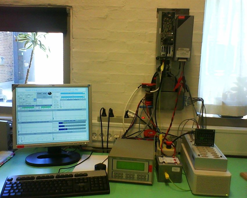
The seventh chapter contains the description of the setup in the laboratory.
Moreover, the experimental results, that confirm the simulations, are described and
discussed.
The report ends with conclusions and suggestions for future work.
vvi
Contents

1   Introduction                                                                            1
    1.1   Background . . . . . . . . . . . . . . . . . . . . . . . . . . . . . . . . .      1
    1.2   Project Motivation . . . . . . . . . . . . . . . . . . . . . . . . . . . . .      2
    1.3   Problem Formulation . . . . . . . . . . . . . . . . . . . . . . . . . . . .       2
    1.4   Project Limitations . . . . . . . . . . . . . . . . . . . . . . . . . . . . .     3
    1.5   Outline of the project . . . . . . . . . . . . . . . . . . . . . . . . . . . .    3

2   Damping Methods of the LCL Filter Resonance                                             5
    2.1   Background . . . . . . . . . . . . . . . . . . . . . . . . . . . . . . . . .      5
    2.2   Passive Damping . . . . . . . . . . . . . . . . . . . . . . . . . . . . . .       5
    2.3   Active Damping . . . . . . . . . . . . . . . . . . . . . . . . . . . . . . .      7

3   Filter Design                                                                          13
    3.1   Filter topology . . . . . . . . . . . . . . . . . . . . . . . . . . . . . . .    13
    3.2   Transfer function of the LCL filter . . . . . . . . . . . . . . . . . . . . .    16
    3.3   Requirements concerning the power delivered to the grid . . . . . . . . .        18
    3.4   Limits on the filter parameters . . . . . . . . . . . . . . . . . . . . . . .    19
    3.5   Calculation of the filter values . . . . . . . . . . . . . . . . . . . . . . .   19
    3.6   Sampling frequency selection . . . . . . . . . . . . . . . . . . . . . . . .     22

4   Control Design                                                                         25
    4.1   Phase-Locked-Loop (PLL) . . . . . . . . . . . . . . . . . . . . . . . . .        26
    4.2   Current Control . . . . . . . . . . . . . . . . . . . . . . . . . . . . . . .    27

                                              vii
CONTENTS
4.3 DC Voltage Control . . . . . . . . . . . . . . . . . . . . . . . . . . . . . 36
5 Active Damping 39
5.1 Notch Filter . . . . . . . . . . . . . . . . . . . . . . . . . . . . . . . . . 39
5.2 Virtual Resistance . . . . . . . . . . . . . . . . . . . . . . . . . . . . . . 43
6 Simulation results 47
6.1 Simulation of a grid connected system using LCL filter . . . . . . . . . . 47
6.2 Active Damping of the LCL filter resonance . . . . . . . . . . . . . . . . 51
7 Experimental Results 57
7.1 Experimental setup . . . . . . . . . . . . . . . . . . . . . . . . . . . . . 57
7.2 Implementation of the Control System . . . . . . . . . . . . . . . . . . . 59
7.3 Tests of the current control loop . . . . . . . . . . . . . . . . . . . . . . 60
7.4 Active Damping of the LCL filter resonance . . . . . . . . . . . . . . . . 64
8 Conclusions and Future Work 67
8.1 Conclusions . . . . . . . . . . . . . . . . . . . . . . . . . . . . . . . . . 67
8.2 Future work . . . . . . . . . . . . . . . . . . . . . . . . . . . . . . . . . 68
A Matlab/Simulink models 79
B Contents of the CD-ROM 83
viiiIntroduction 1
1.1 Background
The energy demand has increased in the last years as a result of the industrial
development, and is predicted to continue increasing, by at least 50% in the next 10 years.
This has focused more research attention on distributed power generation systems like
wind turbines, photovoltaic systems, fuel cells, etc. [1]
Fig. 1.1 shows the block diagram of a distributed power generation system (DPGS).
Figure 1.1: Block diagram of a DPGS.
The main components of a DPGS are:
• Input Power Sources: As shown also in the block diagram, the input power for
a DPGS can come from a wind turbine, a photovoltaic panel, a fuel cell or other
renewable energy sources. The wind turbine converts the motion of the wind into
rotational energy, that can drive an electrical generator. The PV cell is a device
that produces electricity when it is exposed to sunlight. The fuel cell is a chemical
device, which produces electricity directly, without any intermediate stage. These
are the three most used renewable power sources [2],[3].
• Power Converter: The most commonly used topology for the power converter is
the two-level converter, that consists of six switches. An alternative is the three-
level inverter, which contains twice as many transistors. Currently, the interest for
multi-level power converters has grown. These converters consist of six or more
switches per leg, and the main idea is to create a higher number of output voltage
levels, in an attempt to decrease the harmonic content.
• Filter: LCL filters have good performances in current ripple attenuations, but they
introduce a resonance frequency in the system. Two types of methods are used
11 Introduction
in order to damp this frequency: passive damping methods and active damping
methods.
• Grid: A large range of grid impedance values can affect the control of the power
converter and, also, can raise new challenges in the design of the filter.
• Control: The most used control strategy is the voltage oriented control, but other
controls, like the Adaptive Band Hysteresis (ABH) control and Direct Power
Control (DPC), are also implemented.
1.2 Project Motivation
In order to reduce the current harmonics around the switching frequency, a large
input inductance can be connected in the system. But a big inductance will reduce the
system dynamics and the operation range of the converter.[4]
Therefore, instead of using just an inductance, a third order LCL filter can be used
with good performances in current ripple attenuation even for small inductances. How-
ever, LCL filters bring an undesired resonance effect that generates stability problems.
These problems can be solved by using a damping resistor - method called in the literature
"passive damping". Although this method has its advantages like reliability and simplicity,
it has also disadvantages like increased losses through heat dissipation, which leads to
further costs for designing and building a cooling system.
This is the reason why the so-called "active damping methods"have been developed.
These methods modify the control algorithm, stabilizing the system without increasing the
losses.
The most common active damping methods are:
• virtual resistor
• lead-lag element
• filters
1.3 Problem Formulation
The problem formulation for this project is how to control an inverter connected to
the grid through an LCL filter so that the filter resonance would be actively damped.
The block diagram in Fig. 1.1shows the system considered in this project.
The project goals are as follows:
21 Introduction
• investigate and review different active damping methods;
• design the LCL filter;
• model and analyze a system with a grid-connected inverter controlled with an active
damping method;
• implement an active damping method in the laboratory, using an experimental
setup, based on a dSpace control board;
1.4 Project Limitations
The design of the filter and the simulations are carried out on a system with a
rated power of 100 kW. However, for the laboratory implementation, a downscaling of
the system has been done, due to physical contstraints. The following rating of the system
has been used:
• Nominal power: 2.2 kW
• Nominal current: 4.3 A
• Grid voltage: 3x230 V
• DC link voltage: 650 V
• LCL filter components: Li = 6.9mH, Cf = 4.7µF , Lg (= Ltransf ormer ) = 2mH
1.5 Outline of the project
This project is structured in 8 main chapters:
• Chapter 1 is an introduction to the project, containing a short background, the
project motivation and the goals of the project.
• Chapter 2 is a brief study of different methods (both passive and active) to achieve
damping of the resonance frequency of the LCL filter.
• Chapter 3 deals with the design of the filter, including the derivation of the transfer
function and the calculation of the filter parameters.
• In Chapter 4, the design of the control loops is carried out, containing the design
of the phase-locked loop, the current loop and the dc voltage loop.
• In Chapter 5, two active damping methods (the notch filter and the virtual
resistance) are further described and tested in different situations .
31 Introduction
• In Chapter 6, the simulation of the inverter connected to the grid through an LCL
filter is carried out and the results are presented. Also, the active damping of the
filter resonance is implemented and the results are discussed.
• Chapter 7 deals with the description of the test setup and of the results obtained
in the laboratory, concerning both the design of the current control and the
implementation of active damping.
• Chapter 8 is the conclusions, which includes also the future work.
4Damping Methods of the LCL
Filter Resonance 2
In this chapter, different damping methods are described shortly. The damping
methods of the LCL filter resonance can be classified into two classes: passive methods
and active methods.
2.1 Background
The system considered is the one in Fig. 2.1. The control of the grid-connected
inverter is a classical one, with an inner current control loop and an outer voltage control
loop, that keeps a constant value of the dc link voltage and provides the reference current
for the current loop. Also, a grid synchronization method (phase-locked loop) is used in
order to synchronize the control with the phase angle of the grid [5],[2].
Figure 2.1: Control of a grid connected VSI.
2.2 Passive Damping
Passive damping is achieved by adding a resistance in series or in parallel with the
capacitance or inductance of the filter. The four possible positions are shown in Fig. 2.2
52 Damping Methods of the LCL Filter Resonance
Figure 2.2: The possible positions for the damping resistance.
The effects of the damping resistance placed in each of the four positions is shown
in Fig. 2.3, as follows:
Bode Diagram
Bode Diagram
From: Constant1 (pt. 1) To: PLANT (pt. 1)
50 From: Constant1 (pt. 1) To: PLANT (pt. 1)
50
0
Magnitude (dB)
0
Magnitude (dB)
−50 −50
Rd=0.001Ω −100
Rd=10000Ω
−100 Rd=1Ω
Rd=100Ω
Rd=10Ω −150
Rd=10Ω
−150
180 −200
180
90
Phase (deg)
90
Phase (deg)
0
0
−90
−90
−180
0 1 2
Frequency (Hz)103 4 5 −180
10 10 10 10 10 0 1 2 3
Frequency 4 5 6
10 10 10 10 (Hz) 10 10 10
(a) Damping resistance placed in series with the (b) Damping resistance placed in parallel with the
filter inductance. filter inductance.
Bode Diagram
From: Constant1 (pt. 1) To: PLANT (pt. 1) Bode Diagram
50 From: Constant1 (pt. 1) To: PLANT (pt. 1)
50
0
Magnitude (dB)
0
Magnitude (dB)
−50
−50
−100 Rd=0.001Ω
Rd=10000Ω
Rd=1Ω
−150 −100 Rd=100Ω
Rd=10Ω
Rd=10Ω
−200
180 −150
180
90 90
Phase (deg)
Phase (deg)
0 0
−90 −90
−180 −180
0 1 2 3
Frequency 4 5 6
10 (Hz)
0 1 2
Frequency (Hz)103 4 5
10 10 10 10 10 10 10 10 10 10 10
(c) Damping resistance placed in series with the (d) Damping resistance placed in parallel with the
filter capacitance. filter capacitance.
Figure 2.3: Bode plots of LCL filter with passive damping.
The losses on the damping resistance of the LCL filter can be calculated with the
formula:
62 Damping Methods of the LCL Filter Resonance
X
Pd = 3 · Rd · [ii (h) − ig (h)]2 (2.1)
h
where h is the harmonic order.
2.3 Active Damping
2.3.1 Virtual resistance method
As mentioned before, the resonance frequency of an LCL filter can be damped
by connecting a resistor to the filter. But this would greatly reduce the efficiency of the
system. If instead of a real resistance, a virtual resistance is used, the transients can be
damped with no efficiency losses [6], [7], [8], [9].
The single phase equivalent circuit of the AC side and the block diagram is the one
depicted in Fig. 2.4. The current source ii represents the fundamental component of the
phase output current of the VSI and is assumed to be the same as the reference current
used in the control loop. Also, vg is the phase grid voltage.
Figure 2.4: a) Single-phase equivalent circuit of the AC side of the inverter. b) Associated block
diagram.
According to [6], there are four possible topologies concerning the position of the
virtual resistor, the same as for the passive damping (Fig. 2.2).
If the virtual resistor is connected in series with the inductance or the capacitance,
an additional current sensor is needed and if the virtual resistor is connected in parallel
with the inductance or the capacitance, an additional voltage sensor is required.
The concept of the virtual resistance is explained in the following for the first case
(virtual resistance connected in series with the filter inductance). For the other cases, the
same aproach can be used [7].
As seen in Fig. 2.5.a), the resistor connected in series with the filter inductance has
the role of reducing the voltage across this inductance, by a voltage proportional to the
72 Damping Methods of the LCL Filter Resonance
current that flows through it. In the control loop, the current through the filter inductance
is measured and differentiated by a constant of sCf R1 . However, a real resistance is not
used. The differentiator output is injected in the reference current signal of the converter
[6], [7].
Figure 2.5: Block diagrams of the system using the virtual resistor method.
In practice, more virtual resistors can be used at the same time. In the case of using
the virtual resistors connected as in Fig. 2.5.a) and b), the diagram of the control loop is
the one in Fig. 2.6.
If the virtual resistor is connected in series with the filter inductance or filter
capacitance, then the control requires an additional current sensor and a differentiator.
The differentiator might bring noise problems as it amplifies high-frequency signals. If
the virtual resistor is connected in parallel with the filter inductance or filter capacitance,
then the control requires an additional voltage sensor and an amplifier.
Figure 2.6: Block diagram of the controller.
82 Damping Methods of the LCL Filter Resonance
Fig. 2.7 shows a comparison between the Bode Plots of the undamped system and
of the system actively damped using a virtual resistor connected in series with the filter
capacitance.
Bode Diagram Bode Diagram
From: Constant1 To: PLANT From: Constant1 To: PLANT
40 50
20
0
Magnitude (dB)
Magnitude (dB)
0
-20 -50
-40
-100
-60
-80 -150
0 0
-45
Phase (deg)
Phase (deg)
-90 -90
-135
-180 -180
-225
-270 -270
-1 0 1 2 3 4 -1 0 1 2 3 4 5
10 10 10 10 10 10 10 10 10 10 10 10 10
Frequency (Hz) Frequency (Hz)
(a) Bode Plot of the undamped system. (b) Bode Plot of the system actively damped using a
virtual resistor
Figure 2.7: Comparison of Bode Plots.
2.3.2 Lead-Lag Compensator
The shift in the phase angle introduced by the filter can be compensated with an
lead-lag compensator [10],[8]. The lead compensator has the following equation :
Td s + 1
L(s) = kd (2.2)
αTd s + 1
The lead compensator adds positive phase to the system. The compensator needs to
be tuned to the resonance frequency of the filter.[8]
Fig. 2.8 shows the Bode Plots of the undamped system, of the lead compensator and
of the system actively damped using a lead compensator.
9undamped
notch filter
damped
2 Damping Methods of the LCL Filter Resonance
lead-lag
Figure 2.8: Bode Plot of the system damped using a lead compensator.
An active damping method using a lead-lag compensator is described in [10].
This method uses a lead-lag element in the synchronous reference frame applied to the
feedback from the capacitor voltage (Fig. 2.9).
Figure 2.9: Control system with lead-lag compensator.
The grid voltages are used both for the grid synchronization and for the active
damping. First, they are transformed in the reference frame the controller works with
and then inputed to a lead-lag block. Then, the output from the lead-lag block are added
to the output of the current regulators and then processed to obtain the duty cycles to be
sent to the inverter.
In [8], another active damping method with a lead-lag compensator is proposed, in
which the only sensors used are for the output currents and the dc bus voltage, as it can
be seen in Fig. 2.10
102 Damping Methods of the LCL Filter Resonance
Figure 2.10: Sensorless control system with lead-lag compensator.
In this method, the capacitor voltage is estimated with the virtual flux aproach [8].
The signal outputed by the Virtual Flux block is compensated using a Lead-Lag element,
and then added to the output of the current controller.
2.3.3 Notch filter
This method consists of adding a filter in series with the reference voltage of the
modulator (Fig. 2.11).
Figure 2.11: Control system with notch filter.
The basic idea can be explained in the frequency domain by introducing a negative
peak (notch) in the system, that compensates for the resonant peak due to the LCL filter
[11]. This can be done by adding a notch filter in the current loop. The frequency of
the Notch filter has to be tuned at the resonance frequency of the LCL filter, in order to
provide a good damping.
112 Damping Methods of the LCL Filter Resonance
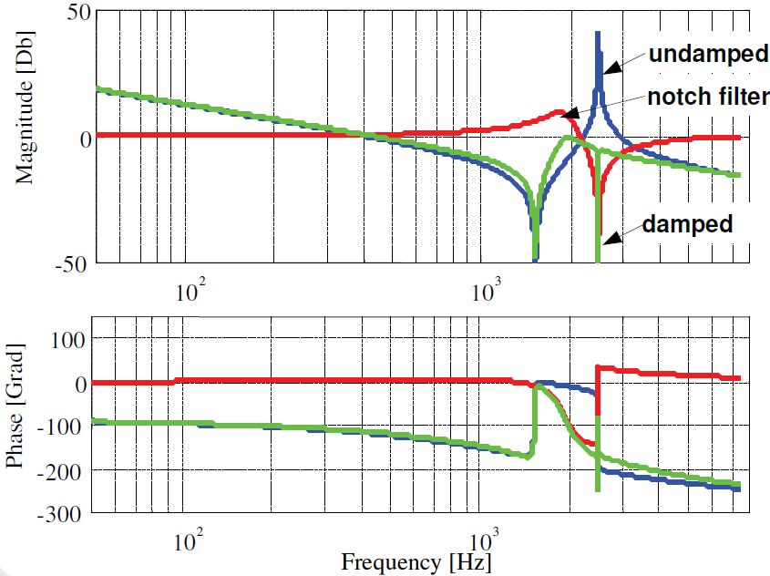
The LCL filter in Fig. 2.12 has a resonance frequency of 4kHz, and the Notch filter
introduces a notch at this frequency. This Bode plot shows the the frequency response of
the undamped system, of the notch filter and of the system actively damped using a notch
filter.
Bode Diagram
From: Frequency1 (pt. 1) To: Circuit (pt. 1)
20
0
Magnitude (dB)
−20
−40 LCL+grid
Notch Filter (NF)
−60
LCL+grid+NF
−80
90
0
Phase (deg)
−90
−180
−270
−360
−450
0 1 2 3 4
10 10 10 10 10
Frequency (Hz)
Figure 2.12: Bode Plot of the system damped a Notch filter[12].
12Filter Design 3
This chapter deals with the mathematical modeling of the LCL filter and the design
of the appropriate values of its components for a power level on 100 kW.
3.1 Filter topology
The filters connected to the inverter output have basically a four-pole topology [13],
like the one in Fig. 3.1.
Figure 3.1: Circuit configuration of a three element filter [13].
3.1.1 L Filter
In this configuration, Zi is finite, Zp is infinite and Zg =0 (Fig. 3.2), meaning that
the filter consists only of an inductance in series with the inverter.
Figure 3.2: Circuit with L filter.
One of the disadvantages of this topology, is the poor system dynamics due to the
voltage drop on the inductance that causes big response times.
133 Filter Design
Also, as it can be seen from the Bode plot (Fig. 3.3), in the case of L filters, the
damping is increased by 20db/dec. Therefore, in order to obtain a good damping, a large
filter (that can be bulky and expensive) has to be used.
Bode Diagram
From: Constant1 To: PLANT
40
20
Magnitude (dB)
0
-20
-40
-60
0
Phase (deg)
-45
-90
-1 0 1 2 3 4
10 10 10 10 10 10
Frequency (Hz)
Figure 3.3: Bode plot of an L Filter.
3.1.2 LC Filter
In this configuration, Zi is finite, Zp is finite and Zg =0, meaning that the filter
consists of an inductance in series with the inverter and a capacitance in parallel (Fig. 3.4).
By using this parallel capacitance, the inductance can be reduced, thus reducing costs and
losses.
Figure 3.4: Circuit with LC filter.
By using a large capacitance, other problems might appear, like high inrush currents,
high capacitance current at the fundamental frequency, or dependence of the filter on the
grid impedance for overall harmonic attenuation [13].
143 Filter Design
The Bode plot of the LC filter is shown in Fig. 3.5.
Bode Diagram
From: Constant1 To: PLANT
40
20
Magnitude (dB)
0
-20
-40
-60
0
Phase (deg)
-90
-180
-270
-1 0 1 2 3 4
10 10 10 10 10 10
Frequency (Hz)
Figure 3.5: Bode plot of an LC Filter.
3.1.3 LCL Filter
Like in the case of the LC filter, the increase in the size of the capacitance leads to
a reduction in the cost and weight of the filter.
Figure 3.6: Circuit with LCL filter.
The LCL filter (Fig. 3.6) brings the advantage of providing a better decoupling
between the filter and grid impedance (as it reduces the dependence of the filter on the
grid parameters) and a lower ripple of the current stress across the grid inductor [13].
153 Filter Design
Bode Diagram
From: Constant1 To: PLANT
40
20
Magnitude (dB) 0
-20
-40
-60
-80
0
Phase (deg)
-90
-180
-270
-1 0 1 2 3 4
10 10 10 10 10 10
Frequency (Hz)
Figure 3.7: Bode plot of an LCL Filter.
3.2 Transfer function of the LCL filter
In order to obtain the transfer function of the LCL filter, the one phase electrical
diagram in Fig. 3.8 is considered. The components of the filter on each phase are
considered to be identical, so the circuit below is suitable for the other two phases.
Figure 3.8: One phase electrical circuit of an LCL filter.
Using Kirchoff’s laws, the filter model in s-plane can be written with the following
equations:
ii − ic − ig = 0 (3.1)
vi − vc = ii (sLi + Ri ) (3.2)
163 Filter Design
vc − vg = ig (sLg + Rg ) (3.3)
1
vc = ic ( + Ri ) (3.4)
sCf
The following notations have been made:
- vi inverter voltage
- ii inverter current
- vc voltage drop on filter capacitance
- ic current accross filter capacitance
- vg grid voltage
- ig grid current
- Li filter inductance on inverter side
- Ri inverter side parasitic resistance
- Cf filter capacitance
- Rc parasitic resistance of filter capacitance
- Lg filter inductance in grid side
- Rg grid side parasitic resistance
The block diagram of the filter is shown in Fig. 3.9
Figure 3.9: Block diagram an LCL filter.
The transfer function of the filter is expressed by:
173 Filter Design
ig
HLCL = (3.5)
vi
In order to compute the transfer function of the filter, some mathematical calcula-
tions have to be made. The grid voltage is assumed to be an ideal voltage source and it
represents a short circuit for harmonic frequencies, and for the filter analysis it is set to
zero: vg = 0.
From the equations (3.3) and (3.4), the following relation can be written:
1 s2 Cf Lg + sCf Rg
ig (sLg + Rg ) = ic ( + Rc ) ⇒ ic = ig (3.6)
sCf sCf Rc + 1
Equation (3.2) can be written as:
vi = vc + ii (sLi + Ri ) (3.7)
By introducing (3.3), (3.1) and (3.6) into the above relation, the inverter voltage can
be written as:
s2 Cf Lg + sCf Rg
vi = ig (sLg +Rg )+(ig +ic )(sLi +Ri ) = ig (sLg +Rg )+(ig +ig )(sLi +Ri )
sCf Rc + 1
(3.8)
(sLi + Ri )(s2 Cf Lg + sCf Rg )
⇒ vi = ig (sLg + Rg + sLi + Ri + ) (3.9)
sCf Rc + 1
So, considering (3.5), the transfer function of the filter can be calculated as:
sRc Cf + 1
H=
s3 Lg Li Cf + s2 Cf (Lg (Rc + Ri ) + Li (Rc + Rg )) + s(Lg + Li + Cf (Rc Rg + Rc Ri + Rg Ri )) + Rg + Ri
(3.10)
3.3 Requirements concerning the power delivered to the
grid
When studying the grid compatibility of a device, the following issues need to
be addressed: average and maximum power produced, reactive power level, grid short-
circuit current (weak or stiff grid conditions), voltage fluctuations, coupling procedure to
the grid, flicker and harmonics[14].
The IEEE Standard 519-1992[14] provides a table which presents the limits for the
total harmonic distortion (THD) of the currents, for a voltage level of below 69kV.
183 Filter Design
Maximum Harmonic Current Distortion in Percent of IL
Individual Harmonic Order (Odd Harmonics)
Isc /IL < 11 11 ≤ h < 17 17 ≤ h < 23 23 ≤ h < 25 35 ≤ h T DD
< 20 4.0 2.0 1.5 0.6 0.3 5.0
20 < 50 7.0 3.5 2.5 1.0 0.5 8.0
50 < 100 10.0 4.5 4.0 1.5 0.7 12.0
100 < 1000 12.0 5.5 5.0 2.0 1.0 15.0
> 1000 15.0 7.0 6.0 2.5 1.4 20
Even harmonics are limited to 25% of the odd harmonics limits above.
Table 3.1: Current distortion Limits for GEneral Dist. Systems (120V - 69 000V)[14]
The ratio Isc /IL is the ratio of the short-circuit current available at the point of
common coupling (PCC), to the maximum fundamental load current.
The limits listed in the table above have been calculated for six-pulse rectifiers so,
when converters with another number p of pulses (q) are used, the limits of the harmonic
orders are increased by a factor of q/6 [14].
3.4 Limits on the filter parameters
In the technical litarature there are many suggestions that may be considered
designing an LCL filter [15],[13],[16],but there is no designated step-by-step strategy on
this matter. However, in this project the following limitations on the filter parameters have
been taken into account [15]:
• the value of the capacitance is limited by the decrease of the power factor, that has
to be less than 5% at the rated power;
• the total value of the filter inductance has to be less than 0.1 p.u. for low power
filters. However, for high power levels, the main aim is to avoid the saturation of
the inductors;
• the resonance frequency of the filter should be higher than 10 times the grid
frequency and than half of the switching frequency.
3.5 Calculation of the filter values
The system parameters considered for the calculation of the filter components, for
a power level of 100kVA, are presented in the table bellow.
193 Filter Design
Grid Line to Line Voltage En = 380V
Output Power of the Inverter Sn = 100kVA
DC-Link Voltage Vdc = 650V
Frequency of grid voltage f = 50Hz
Switching frequency fsw = 3kHz
Table 3.2: Parameters of the considered system.
For the further development, the base values are calculated, as the filter values are
reported as a percentage of these.
(En )2
Zb = = 1.444[Ω] (3.11)
Sn
Zb
Lb = = 4.596[mH] (3.12)
ωn
1
Cb = = 2204.3621[µF ] (3.13)
ωn Zb
The first step is to design the inverter side inductance, which is determined by [15]:
ii (nsw ) 1
≈ (3.14)
vi (nsw ) ωsw Li
where ωsw is the switching frequency and nsw is the frequency multiple of the
fundamental frequency at the switching frequency.
According to equation (3.14), a current ripple on the inverter side of 1% is obtained
with an inductance Li = 530µH(11.53%).
A filter capacitance Cf = 110µF fulfills the requirement on the power factor stated
before.
A ripple attenuation of 20% is selected on the grid side with respect to the current
ripple on the inverter side. The dependency of the ripple attenuation to the inductance
ration is depicted in Fig. 3.10
203 Filter Design
1
0.8
igrid(h)/iinv(h)
0.6
0.4
0.2
0
0 0.2 0.4 0.6 0.8 1 1.2 1.4 1.6 1.8 2
r
Figure 3.10: Current ripple attenuation as a function of the inductance ratio for 100kVA.
The ripple attenuation of 20% is obtained with a ratio of r = 0.32. This means that
the grid side inductance Lg is equal to r · Li ≈ 170µH(3.69%).
Having chosen the filter values, the resonance frequency of the filter can be
calculated as:
s
Li + Lg
ωres = = 14.97 · 103 ⇒ fres = 1.337[kHz] (3.15)
Li · Lg · Cf
The zero-pole map in Fig. 3.11 and the Bode plot of the designed filter is depicted
in Fig. 3.12 and .
Pole-Zero Map
1
0.25/T
0.30/T 0.20/T
0.8 0.35/T 0.1
0.15/T
0.2
0.6 0.3
0.40/T 0.4 0.10/T
0.5
0.4 0.6
Imaginary Axis
0.7
0.45/T 0.8 0.05/T
0.2 0.9
0.50/T
0
0.50/T
-0.2
0.45/T 0.05/T
-0.4
0.40/T 0.10/T
-0.6
-0.8 0.35/T 0.15/T
0.30/T 0.20/T
0.25/T
-1
-1 -0.5 0 0.5 1
Real Axis
Figure 3.11: Zero-Pole Map of the LCL filter for a power level of 100kVA.
213 Filter Design
Bode Diagram
100
80 System: H_LCL
Frequency (Hz): 1.34e+003
60 Magnitude (dB): 44.3
Magnitude (dB)
40
20
0
-20
-40
-60
-80
-100
0
-45
Phase (deg)
-90
-135
-180
-225
-270
-2 -1 0 1 2 3 4
10 10 10 10 10 10 10
Frequency (Hz)
Figure 3.12: Bode plot of the designed LCL filer for a power lever of 100kVA.
3.6 Sampling frequency selection
An issue that needs to be considered before begining to design the control of
the system, is to choose the optimal sampling frequency of the control system. The
low resonance frequency of the filter imposes some limits on the range of sampling
frequencies of the control.
Fig. 3.13 show the root loci of the open loop PI current control, plotted at different
sampling frequencies. As it can be seen, if a sampling frequency fs of 2000Hz is chosen,
the system is always unstable, as the resonance poles given by the filter are always out of
the unity circle.
In the case of fs = 3000Hz to fs = 4000Hz, the system is stable for a large range
of Kp . As the sampling frequency increases, the system remains stable for a lower and
lower range of Kp , as it is the case with the sampling frequency of 5000Hz.
223 Filter Design
Root Locus Editor for Open Loop 1 (OL1)
Root Locus Editor for Open Loop 1 (OL1)
1 500
600 400 1 750
900 600
0.8 700 0.1 300
0.2 0.8 1.05e3 0.1 450
0.3 0.2
0.6
800 0.4 200 0.3
0.6
1.2e3 0.4 300
0.5
0.4 0.6 0.5
0.7 0.4 0.6
900 100 0.7
0.8
1.35e3 150
0.2 0.9
0.8
0.2
Imag Axis
0.9
Imag Axis
1e3
0 1e3 1.5e3
0 1.5e3
-0.2
-0.2
900 100
1.35e3 150
-0.4
-0.4
800 200
-0.6 1.2e3 300
-0.6
-0.8 700 300 1.05e3 450
-0.8
600 400 900 600
500 750
-1 -1
-1 -0.8 -0.6 -0.4 -0.2 0 0.2 0.4 0.6 0.8 1 -1 -0.8 -0.6 -0.4 -0.2 0 0.2 0.4 0.6 0.8 1
Real Axis Real Axis
(a) Root locus at fs = 2000Hz. (b) Root locus at fs = 3000Hz.
Root Locus Editor for Open Loop 1 (OL1)
1 Root Locus Editor for Open Loop 1 (OL1)
1e3
1.2e3 800
1 1.25e3
0.8 1.4e3 0.1 600 1.5e3 1e3
0.2
0.8 1.75e3 0.1 750
0.3
0.6 0.2
1.6e3 0.4 400
0.3
0.5 0.6
2e3 0.4 500
0.4 0.6
0.5
0.7
1.8e3 200 0.4 0.6
0.8 0.7
0.2 0.9 2.25e3 250
0.8
Imag Axis
0.2 0.9
Imag Axis
2e3
0 2e3
2.5e3
0 2.5e3
-0.2
1.8e3 200 -0.2
2.25e3 250
-0.4
-0.4
1.6e3 400
-0.6 2e3 500
-0.6
-0.8 1.4e3 600
-0.8 1.75e3 750
1.2e3 800
1e3 1.5e3 1e3
-1 1.25e3
-1
-1 -0.8 -0.6 -0.4 -0.2 0 0.2 0.4 0.6 0.8 1 -1 -0.8 -0.6 -0.4 -0.2 0 0.2 0.4 0.6 0.8 1
Real Axis Real Axis
(c) Root locus at fs = 4000Hz. (d) Root locus at fs = 5000Hz.
Figure 3.13: Root loci of the open loop current control.
The sampling frequency chosen for this project in order to tune the parameters of
the controller is 3000Hz.
233 Filter Design
24Control Design 4
In this chapter, the control of the inverter is designed. In the first part, the PLL is
described. Then the current loop is designed, for the case of PI control and the case of
P+Resonant control. The last part deals with the design of the dc voltage loop.
The block diagram of the inverter control considered in this project is presented in
Fig. 4.1.
Figure 4.1: Control block diagram of the grid connected-system.
The current is oriented along the active voltage component (Vd ), this is why this
strategy is called voltage oriented control. A PLL alogithm detects the phase angle of the
grid, the grid frequency and the grid voltage. The frequency and the voltage are needed
for monitoring the grid conditions and for complying with the control requirements. The
phase angle of the grid is required for reference frame transformations.
If a PI current control is implemented, then the currents are transformed into the
synchronous reference frame, and the algorithm implements also the decoupling between
the two axes. If a P+Resonant controller is used, then the currents are transformed into
the stationary reference frame and decoupling is not implemented.
For the dc voltage control, a standard PI controller is used also for the DC voltage
and it outputs the reference for the current control [17].
The modulation block calculates the propper states of the switches in order to obtain
the reference input voltage.
254 Control Design
4.1 Phase-Locked-Loop (PLL)
When dealing with the control of grid connected converters, an aspect that needs to
be taken into account is the correct generation of the reference signals, which is obtained
with a fast and accurate detection of the phase angle and the grid frequency and voltage.
One of the methods to synchronize the reference current of the inverter with the grid
voltage, is an algorithm called Phase-Locked-Loop (PLL).
The PLL can be defined as an algorithm that determines a signal to track another, so
that the output signal is synchronized with the input one both in frequency and in phase
[18],[19]. A common way to realize the PLL is in the ’dq’ reference frame.
The block diagram of the PLL algorithm implemented in the synchronous reference
frame, is shownin Fig. 4.2.
Figure 4.2: Block diagram of PLL.
The algorithm uses as input the measured grid voltage, and performs an abc − dq
transformation. The ’phase-lock’ is realised by setting Vq to 0, using a PI controller. The
output of the PI controller is the grid frequency, which, when added to the feed-forward
frequency and integrated, provides the grid phase angle, θ. A modulo division block is
used to aviod θ from getting too big (and, thus, to avoid overflows in fixed-point DSPs).
The transfer function of the PLL can be written as [18]:
Kp
Kp · s + Ti
HP LL (s) = Kp
(4.1)
s2 + Kp · s + Ti
An analogy can be made with a standard second order transfer function that has a
zero:
2ωn ζ · s + ωn2
G(s) = (4.2)
s2 + 2ωn ζ · s + ωn2
The gains of the PI controller can be calculated as functions of the damping factor,
ζ and the settling time, Tset :
264 Control Design
9.2
Kp = (4.3)
Tset
Tset ζ 2
Ti = (4.4)
4.3
4.6
where ωn is the undamped natural frequency and ωn = ζTset
[18].
Selecting a damping factor ζ = 0.707 (which provides an overshoot of less than 5%
in case of a step response), and a settling time Tset = 0.04, the value of the PI gains can
be calculated. The obtained values are: Kp = 230 and Ti = 0.0046 (or Ki = 50000)
The grid phase angle obtained with the described PLL algorithm is the one presented
in Fig. 4.3.
2
Ua
1.5 theta
Grid voltage on phase a [p. u.]
Grid phase angle [p. u.]
1
0.5
0
-0.5
-1
-1.5
0 0.01 0.02 0.03 0.04 0.05 0.06 0.07 0.08 0.09 0.1
t [s]
Figure 4.3: Phase angle of the grid voltage and the grid voltage on phase a.
4.2 Current Control
In this project, two types of current controllers are implemented: a PI control in the
synchronous reference frame and a P+Resonant (PR) control in the stationary reference
frame. The PI current control block diagram is given in Fig. 4.4, and the PR current control
with harmonic compensation block diagram in shown in Fig. 4.5
274 Control Design
Figure 4.4: Block diagram of the inverter PI control.
Figure 4.5: Block diagram of the inverter PR control + Harmonic Compensation.
At first, the controllers are tunned with an analytical method in order to obtain the
values with which the discrete analysis starts. Therefore, the current controllers are firstly
tuned using the optimal modulus criterion [20].
284 Control Design
4.2.1 PI Current Control
The block diagram of the PI regulator is depicted in Fig. 4.6 and the transfer function is
the one in (4.6)
Figure 4.6: Block diagram of PI regulator.
Ki
GP I (s) = Kp + (4.5)
s
The d and q control loops have the same dynamics, so the tuning of the PI
parameters for the current control is done only for the d axis. For the q axis the parameters
are assumed to be the same.
As it can be seen from the current control block diagram in Fig. 4.7, the voltage
feed forward and the decoupling between the d and q axes has been neglected as they are
considered as disturbances.
Figure 4.7: Block diagram of the current control loop.
This diagram can be restructured as the one in Fig. 4.8.
294 Control Design
Figure 4.8: Block diagram of the current control loop - restructured.
In this block diagram, the following blocks are included:
• PI controller block with the transfer function:
Kicrt
GP Icrt (s) = Kpcrt + (4.6)
s
• Control Algorithm block with the transfer function:
1
Gcontrol (s) = (4.7)
1 + sTs
where Ts = 1/fs and fs = 3kHz is the sampling frequency.
• Inverter block with the transfer function:
1
Ginverter (s) = (4.8)
1 + s · 0.5Tsw
where Tsw = 1/(fsw ) and fsw = 3kHz is the switching frequency of the inverter.
• Filter block is a simplified transfer function of the filter, that keeps into account
only the the values of inductances and parasitic resistances:
1
Gf ilter (s) = (4.9)
Ls + R
where L = Li + Lg and R = Ri + Rg
• Sampling block with the transfer function:
1
Gsampling = (4.10)
1 + s · 0.5Ts
304 Control Design
The transfer function of the current loop can be calculated as:
Gcrt = GP Icrt · Gcontrol · Ginverter · Gf ilter · Gsampling (4.11)
Using (4.6), (4.7), (4.8), (4.9) and (4.10), the transfer function of the current loop
can be written in a simplified manner as:
Kpcrt s + Kicrt 1 Ke
Gcrt = (4.12)
s 1 + sT 1 sTe + 1
P
where Ke = 1/R, Te = L/R and TP 1 = Ts + 0.5Tsw + 0.5Ts
Using the optimal modulus criterion [20], the following relation can be written:
Kpcrt s + Kicrt 1 Ke 1
= (4.13)
s 1 + sT 1 sTe + 1
P
2sT 1 (1 + sTP 1 )
P
From (4.13) Kpcrt and Kicrt can be identified and their values calculated, as:
Te
Kpcrt = = 0.5 (4.14)
2Ke TP 1
Kpcrt
Kicrt = = 2.15 (4.15)
Te
These values are used to start the discrete analysis (using the pole placement
method) using the Matlab toolbox, Sisotool. The requirements imposed on the current
controller are:
• the current loop should be stable, with a phase margin larger than 45◦ and a gain
margin larger than 6dB.
• the bandwidth of the system should be minimum 500 Hz.
Using the root locus method, the proportional gain Kp is selected so that the
dominant poles have a damping factor higher 0.7. As shown in Fig. 4.9, with a Kp value
of 0.67, the damping of the resonant poles reaches the value of 0.9. The integral gain has
been chosen as a tradeoff between a good noise rejection and good dynamics.
The zero-pole map and the Bode plot of the open-loop current control depicted in
Fig. 4.9
314 Control Design
Root Locus Editor for Open Loop 1 (OL1) Open-Loop Bode Editor for Open Loop 1 (OL1)
80
1 750
900 600
0.8 0.1
60
1.05e3 450
Magnitude (dB)
0.2
0.3
0.6 40
1.2e3 0.4 300
0.5
0.4 0.6
20
0.7
1.35e3 150
0.8
0.2 0.9
0
Imag Axis
G.M.: 9.82 dB
Freq: 489 Hz
1.5e3
0 1.5e3
Stable loop
-20
-90
-0.2 -135
1.35e3 150
-180
-0.4 -225
Phase (deg)
-270
1.2e3 300
-0.6 -315
-360
-0.8 1.05e3 450 -405
-450
900 600
750 -495 P.M.: 45 deg
Freq: 1.27e+003 Hz
-1
-540
-1 -0.5 0 0.5 1 -1 0 1 2 3 4
10 10 10 10 10 10
Real Axis Frequency (Hz)
Figure 4.9: Zero-pole map and open-loop Bode plot of the PI current control.
Fig. 4.9 also shows that the control has a phase margin of 45◦ and a gain margin of
9.82dB.
The step response is plotted in Fig. 4.10. It can be seen that a settling time of 0.01
is obtained.
Step Response
1.4
1.2
1
System: Closed Loop r to y
I/O: r to y
Settling Time (sec): 0.0142
0.8
Amplitude
0.6
0.4
0.2
0
0 0.005 0.01 0.015 0.02 0.025 0.03
Time (sec)
Figure 4.10: Step response of the PI current control loop.
324 Control Design
4.2.2 PR Current Control
The block diagram of the PR regulator with Harmonic Compensation is depicted in
Fig. 4.11 .
Figure 4.11: Block diagram of PR regulator.
The transfer function of the PR controller is [21]:
s
GP I (s) = Kp + Ki (4.16)
s2 + ω2
where aw is the anti-windup function implemented as:
ymax − y, y > ymax
aw = (4.17)
y − ymax , y < −ymax
The transfer function of the Harmonic Compensator is[21]:
X s
GHC (s) = KIh 2 , h = 3, 5, 7 (4.18)
s + (ω · h)2
The most important harmonics in the current spectrum are the 3rd, the 5th and
the 7th. So the harmonic compensator is designed to compensate these three selected
harmonics.
In order to perform the discrete analysis on the PR current control, the initial values
calculated with the optimal modulus method for the PI control are used for the PR control
to begin with.
334 Control Design
Using the root locus method, the proportional gain Kp is selected so that the
dominant poles have a damping factor of 0.7. As it can be seen in the Fig. 4.12, with a
Kp value of 0.78, the damping of the resonant poles reaches the value of 0.7. An integral
gain Ki of 300 has been chosen as a tradeoff between a good noise rejection and good
dynamics.
The zero-pole map and the Bode plot of the open-loop current control depicted in
Fig. 4.12
Root Locus Editor for Open Loop 1 (OL1) Open-Loop Bode Editor for Open Loop 1 (OL1)
1 160
750 G.M.: 7.44 dB
900 600 Freq: 479 Hz
140
Stable loop
0.8 1.05e3 450 120
100
Magnitude (dB)
0.6
1.2e3 300
80
0.4 60
1.35e3 150 40
0.2
20
Imag Axis
0
1.5e3 0
1.5e3
-20
0.9 0
-0.2
0.8
1.35e3 150
0.7 -90
-0.4 0.6
-180
Phase (deg)
0.5
1.2e3 0.4 300
-0.6 0.3 -270
0.2
1.05e3 450 -360
-0.8 0.1
900 600 -450
750 P.M.: 46.3 deg
-1 Freq: 181 Hz
-540
-1 -0.8 -0.6 -0.4 -0.2 0 0.2 0.4 0.6 0.8 1 -1 0 1 2 3 4
10 10 10 10 10 10
Real Axis Frequency (Hz)
Figure 4.12: Zero-pole map and open-loop Bode plot of the PR current control.
Fig. 4.12 also shows that the control has a phase margin of 46.3◦ and a gain margin
of 7.44dB.
The Bode plot of closed-loop current control is plotted in Fig. 4.13. It shows that
the bandwidth of the current controller has a value of approximately 500Hz.
344 Control Design
Bode Editor for Closed Loop 1 (CL1)
6
4
2
Magnitude (dB)
X: 439.1
0 Y: -2.752
Z: -4
-2
-4
-6
-8
-10
-12
225
180
135
90
Phase (deg)
45
0
-45
-90
-135
-180
-225
-270
2 3 4
10 10 10
Frequency (Hz)
Figure 4.13: Closed-loop Bode plot of the PR current control.
The step response is plotted in Fig. 4.14. It can be seen that a settling time of 0.02
is obtained.
Step Response
1.4
1.2
System: Closed Loop r to y
I/O: r to y
Settling Time (sec): 0.0202
1
0.8
Amplitude
0.6
0.4
0.2
0
0 0.005 0.01 0.015 0.02 0.025 0.03
Time (sec)
Figure 4.14: Step response of the PR current control loop.
354 Control Design
4.3 DC Voltage Control
As in the case of the dc voltage loop, the controllers are tunned with an analytical method
in order to obtain the values with which the discrete analysis starts. Thus, the dc voltage
controller is tuned using the optimum symmetrical criterion [22].
The closed loop transfer function of the current loop can be written as:
1 0.5sTs + 1
Gcrtclosed = ≈ (4.19)
2sT 1 (1 + sT 1 ) + 1
P P
2sTP 1 + 1
The dc voltage control block diagram is shown in Fig. 4.15.
Figure 4.15: Block diagram of the voltage dc control loop.
This diagram can be restructured as the one in Fig. 4.16.
Figure 4.16: Block diagram of the dc voltage loop - restructured.
The values of the PI controller are calculated using the method called optimum
symmetrical [22]. Firstly, a phase margin ψ of 45◦ is imposed.
Considering
1 + cosψ
a= (4.20)
sinψ
364 Control Design
the PI parameters can be calculated as:
4Cdc
Kpvol = 2
= 2.77 (4.21)
2TP 2 9aTs
Kpvol
Kivol = = 482.2 (4.22)
3 · a2 · Ts
Using the pole placement method, a discrete analysis has been performed with the
Matlab toolbox, Sisotool.
With a proportional gain Kp = 1.7 a stable loop with a phase margin of 59.1◦ and a
gain margin of 18.5dB are obtained, as shown in Fig. 4.17.
Root Locus Editor for Open Loop 1 (OL1) Open-Loop Bode Editor for Open Loop 1 (OL1)
80
1 750
900 600 60
0.8 1.05e3 0.1 450 40
Magnitude (dB)
0.2
0.3
20
0.6 1.2e3 300
0.4
0.5
0
0.4 0.6
-20
0.7
1.35e3 150
0.8
0.2 -40
0.9
Imag Axis
G.M.: 18.5 dB
-60 Freq: 202 Hz
1.5e3
0 1.5e3
Stable loop
-80
-90
-0.2
1.35e3 150
-0.4 -180
Phase (deg)
1.2e3 300
-0.6 -270
1.05e3 450
-0.8 -360
900 600
750 P.M.: 59.1 deg
-1 Freq: 38.4 Hz
-450
-1 -0.5 0 0.5 1 0 1 2 3 4
10 10 10 10 10
Real Axis Frequency (Hz)
Figure 4.17: Zero-pole map and Bode plots of the voltage control loop.
The settling time for the voltage loop is 0.05s. The step response is plotted in
Fig. 4.18.
374 Control Design
Step Response
1.4
1.2
1
System: Closed Loop r to y
I/O: r to y
Settling Time (sec): 0.0507
0.8
Amplitude
0.6
0.4
0.2
0
0 0.01 0.02 0.03 0.04 0.05 0.06 0.07 0.08 0.09
Time (sec)
Figure 4.18: Step response of the voltage control loop.
38Active Damping 5
This chapter deals with the implementation of two active damping methods: notch
filter and virtual resistor. For each of them, the frequency response is studied, as well as
the effect of the changes in the grid values and in the filter parameters.
5.1 Notch Filter
5.1.1 Transfer function and frequency response
As stated before in section 2.3.3, a method to obtain active damping is to introduce
in the current loop a notch filter, tuned at the resonance frequency of the LCL filter.
The transfer function of the notch filter is:
s2 + 2ζ2 ω0 s + ω02
Hnotch (s) = (5.1)
s2 + 2ζ1 ω0 s + ω02
The dependence between ζ1 and ζ2 can be expressed by: [12]
ζ2 < ζ1
(5.2)
ζ2 = ζ1 /α
The term α is related to the resistance of the grid (Rgrid ) and can be expressed as:
α = k· Rgrid (k is a constant). ω0 is the cutooff frequency of the notch filter and is
related to the resonance frequency of the LCL filter.
Considering the LCL filter designed before, in section 3.5, with the transfer function
stated in (3.10) and the transfer function of the notch filter stated in (5.1), the frequency
response of the system can be analised, from the Bode plot depicted in Fig. 5.1.
395 Active Damping
Bode Diagram
From: Constant1 To: PLANT
50
Magnitude (dB)
0
-50
-100
180
Phase (deg)
0
-180
-360
-1 0 1 2 3 4
10 10 10 10 10 10
Frequency (Hz)
Figure 5.1: Bode Plot of LCL filter, notch filter and the two in series.
The notch filter introduces in the system two zeros and two poles. The root loci
and the open loop bode plots without and with the notch filter are shown in Fig. 5.2 and
Fig. 5.3
Root Locus Editor for Open Loop 1 (OL1) Open-Loop Bode Editor for Open Loop 1 (OL1)
1 LCL + grid Dominant 150 G.M.: 8.25 dB
750 Freq: 486 Hz
poles 900 600 poles Stable loop
0.8
Magnitude (dB)
1.05e3 0.1 450
0.2 100
0.3
0.6 1.2e3 0.4 300
0.5
0.4 0.6
50
0.7
1.35e3 0.8 150
0.2
Imag Axis
0.9
0 1.5e3 0
1.5e3
0
-0.2
1.35e3 150
-90
-0.4
Phase (deg)
-180
1.2e3 300
-0.6 -270
-0.8 1.05e3 450 -360
900 600 -450
750 P.M.: 42.7 deg
-1 Freq: 1.28e+003 Hz
-540
-1 -0.5 0 2 4
Real0Axis 0.5 1 10 10 10
Frequency (Hz)
Figure 5.2: Root loci and open-loop Bode diagram of the current loop without notch filter.
405 Active Damping
Root Locus Editor for Open Loop 1 (OL1) Open-Loop Bode Editor for Open Loop 1 (OL1)
1 Notch filter 750 150
900 600 Dominant G.M.: 8.54 dB
zeros Notch Filter poles Freq: 299 Hz
Stable loop
0.8 1.05e3 poles 0.1 450
100
Magnitude (dB)
0.2
0.3
0.6 1.2e3 300
0.4
0.5 50
0.4 0.6
0.7
1.35e3 0.8 150
0.2 0.9 0
Imag Axis
1.5e3
0 1.5e3
-50
0
-0.2
1.35e3 150 -90
Phase (deg)
-0.4 -180
1.2e3 300
-0.6 -270
-360
1.05e3 450
-0.8
-450 P.M.: 43.4 deg
900 600
750 Freq: 118 Hz
-1 -540
-1 -0.5 0 0.5 1 -1 0 1 2 3 4
10 10 10 10 10 10
Real Axis Frequency (Hz)
Figure 5.3: Root loci and open-loop Bode diagram of the current loop with notch filter.
5.1.2 Effect of changes in grid inductance
The fluctuations of the grid inductance affects the resonance frequency, as the
resonance frequency of the filter, considering the grid inductance (Lgrid ), is calculated
as:
s
Li + (Lg + Lgrid )
ωres = (5.3)
Li · (Lg + Lgrid ) · Cf
An increase in the grid inductance leads to a decrease in the resonance frequency and
a decrease in the grid impedance leads to an increase in the resonance frequency. This
means that some kind of grid condition detection algorithm should be used, in order to
accurately tune the notch filter.
Bode Diagram
Bode Diagram From: In(1) To: PLANT
From: In(1) To: PLANT
40
50
20
Magnitude (dB)
Magnitude (dB)
0
0
-50 -20
-40
-100 0
0
-90 -90
Phase (deg)
Phase (deg)
-180
-180 Lgrid = 50µH
-270 Lgrid = 50µH
Lgrid = 200µH Lgrid = 200µH
-360 -270
-450 Lgrid = 500µH Lgrid = 500µH
-360
-540 -2 -1 0 1 2 3 4
-2 -1 0 1
Frequency 2 3 4 10 10 10 10 10 10 10
10 10 10 10 (Hz) 10 10 10
Frequency (Hz)
(a) Grid detection is not used. (b) Grid detection is used.
Figure 5.4: Bode Plots of LCL filter plus grid inductance and notch filter at grid fluctuations.
415 Active Damping
In Fig. 5.4 (a) is shown the frequency response of the LCL filter plus grid impedance
and notch filter, when no grid detection algorithm is used, but just an assumption that the
grid inductance is Lgrid = 50µH. It can be seen that if the grid inductance is a lot different
from the assumption, the notch filter is no longer efficient, as it is tuned on a frequency
which is not the resonance frequency. However, if a grid detection method is used (as it is
the case in Fig. 5.4) (b), then the notch filter effectively damps the resonance frequency.
5.1.3 Effect of changes in the values of LCL filter components
Sometimes, during extensive use, the filter components can sustain changes in their
values, due to high temperatures or ageing. Fig. 5.5 (a) and (b) show how the frequency
response of the LCL filter plus grid impedance and notch filter, changes when the value
of the filter capacitance and the inverter side inductance changes with ±10%.
Bode Diagram Bode Diagram
From: In(1) To: PLANT From: In(1) To: PLANT
40 40
20
20
Magnitude (dB)
Magnitude (dB)
0
0
-20
-20
-40
-60 -40
-80 -60
0 0
-90
-90
Phase (deg)
Phase (deg)
-180
Cf = 110 µF -180
-270 Li = 530 µH
Cf = 100 µF -270
-360 Li = 480 µH
Cf = 120 µF
-450 -360 Li = 580 µH
-540 -450
-1 0 1 2 3 4
10 10 10 10 10 10 -1 0 1 2 3 4
10 10 10 10 10 10
Frequency (Hz) Frequency (Hz)
(a) Cf varies with ±10µF . (b) Li varies with ±50µH.
Figure 5.5: Bode Plots of LCL filter plus grid impedance and notch filter when the LCL filter
components vary.
It can be seen that the change in the capacitance value produces a loss in the
efficiency of the notch filter, though not making its presence completely useless, as a
certain amount of damping still exists. The change in the inductance value has even
smaller effects on the efficiency of the notch filter, because the resonance frequency is
not modified much.
425 Active Damping
5.2 Virtual Resistance
5.2.1 Frequency response
As stated before, the idea of the virtual resistance method is to simulate the behavior
of passive damping, without actually using a damping resistance in the setup. Out of the
four positions the damping resistance can be placed in, two are investigated in this project:
in series with the filter capacitance and in series with the inverter side inductance.
Fig. 5.6.a and Fig. 5.6.b show how the frequency response of the filter is modified
when a virtual damping resistance with different values is used, in the two positions
mentioned before.
Bode Diagram Bode Diagram
From: Constant1 To: PLANT From: Constant1 To: PLANT
40 40
20
Magnitude (dB)
20
Magnitude (dB)
0 0
-20 -20
-40 -40
0 0
-90 -90
Phase (deg)
Phase (deg)
Rd = 0.1 mΩ Rd = 0.002 Ω
-180 Rd = 10 mΩ -180 Rd = 0.1 Ω
Rd =100 mΩ Rd = 0.5 Ω
-270 Rd = 300 mΩ -270 Rd = 1 Ω
Rd = 500 mΩ Rd = 5 Ω
-360 -360
-1 0 1 2 3 4 -1 0 1 2 3 4
10 10 10 10 10 10 10 10 10 10 10 10
Frequency (Hz) Frequency (Hz)
(a) Rd in series with the filter capacitance. (b) Rd in series with the filter inductance.
Figure 5.6: Bode Plots of LCL filter with different damping resistances.
When the virtual damping resistance is connected in series with the filter capac-
itance, the attenuation around the switching frequency, gets lower as the resistance is
increased. When the damping resistance is connected in series with the inverter side
inductance, the attenuation remains the same around the switching frequency, but the
resonance frequency is decreased as the resistance is increased.
The root loci plots show that the effect of virtual damping resistance in the control
loop attracts the resonant poles of the filter towards the inside of the circle, providing a
considerable amount of damping. The root loci and the open loop bode plots of the system
with virtual damping resistance connected in series with the filter capacitance and with
the inverter side inductance are shown in Fig. 5.7 and Fig. 5.8
435 Active Damping
Root Locus Editor for Open Loop 1 (OL1) Open-Loop Bode Editor for Open Loop 1 (OL1)
150
1 750 G.M.: 8.21 dB
900 600 Freq: 482 Hz
Stable loop
0.8 1.05e3 450 100
Magnitude (dB)
Rd
0.6
1.2e3 300
50
0.4
1.35e3 150
0.2 0
Imag Axis
1.5e3
0 1.5e3
-50
0.9 0
-0.2
1.35e3 0.8 150
0.7 -90
-0.4 0.6
0.5
-180
Phase (deg)
1.2e3 0.4 300
-0.6 0.3
-270
0.2
-0.8 1.05e3 0.1 450 -360
900 600
-1
750 -450 P.M.: 51.3 deg
Freq: 171 Hz
-540
-1 -0.5 0 0.5 1 -1 0 1 2 3 4
10 10 10 10 10 10
Real Axis Frequency (Hz)
Figure 5.7: Root loci and open-loop Bode diagram of the current loop with virtual damping
resistance in series with Cf .
Root Locus Editor for Open Loop 1 (OL1) Open-Loop Bode Editor for Open Loop 1 (OL1)
140
1 750 G.M.: 12.4 dB
900 600 120 Freq: 588 Hz
Stable loop
0.8 1.05e3 450 100
Magnitude (dB)
0.6 Rd 80
1.2e3 300
60
0.4
40
1.35e3 150
0.2 20
Imag Axis
1.5e3 0
0 1.5e3
-20
0.9 90
-0.2
1.35e3 0.8 150
0.7 0
-0.4 0.6
0.5 -90
Phase (deg)
1.2e3 0.4 300
-0.6 0.3 -180
0.2 -270
-0.8 1.05e3 0.1 450
-360
900 600
750
-1 -450 P.M.: 95.5 deg
Freq: 58.6 Hz
-540
-1 -0.5 0 0.5 1 1 2 3 4
10 10 10 10
Real Axis Frequency (Hz)
Figure 5.8: Root loci and open-loop Bode diagram of the current loop with virtual damping
resistance in series with Li .
5.2.2 Effect of changes in the grid inductance
Like for the notch filter method, the effect of the changes in the grid inductance
changes is studied, in the case of virtual damping resistance connected in series with the
filter capacitance and with the grid side inductance.
The tests have been performed with a virtual damping resistance of 300mΩ when
the resistance was in series with the filter capacitance, and a virtual damping resistance of
5Ω when the resistance was in series with the grid side inductance.
44You can also read