B.Tech (ECE) VI Sem Unit-3 VLSI Technology (BEC-35) - Classification of Lithography and Its Properties Photo-Masks and Photo-resists (PR) Part-III ...
←
→
Page content transcription
If your browser does not render page correctly, please read the page content below
B.Tech (ECE) VI Sem
              Unit-3
     VLSI Technology (BEC-35)
Classification of Lithography and Its Properties
       Photo-Masks and Photo-resists (PR)

                   Part-III
               March-April 2020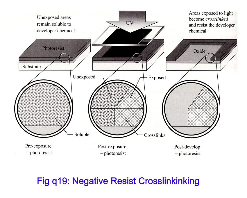
2
Step No. 6: Pattern Development
• Purpose: to develop the
  desired pattern in the
  Photo-resist
• Equipment: Baths for
  developing and
  cleaning chemicals and
  spin dryer

• Method: Dip the wafer
  in the developing and
  rinsing chemicals for
  desired times and then
  spin dry.                       3
4
5
Step No. : Hard Bake
Purpose:
    To remove water and any other liquid and
    to harden the photoresist present on the
    wafer.
Equipment:
    Oven
Method:
    Heat at ~ 200 C for about 20 minutes
                                           6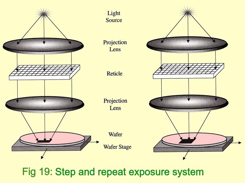
Step No. : Develop Inspect

Optical Inspection under microscope
(100X) is done to check for
      • Line Resolution
      • Line Width
      • Resolution
      • Particles and Defects

                                      7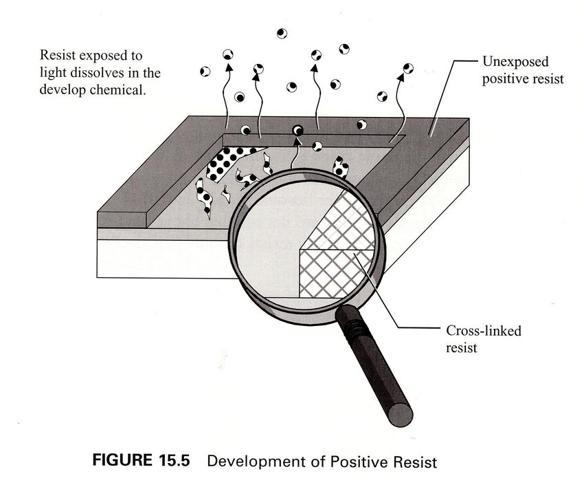
What is Photoresist?
• The  photosensitive compound used             in
 microelectronics is called Photoresist.

• Certain properties of these compounds change
 when they are exposed to light of a particular
 wave length.

• Photoresists are used to transfer the pattern on
                                                8
 the substrate.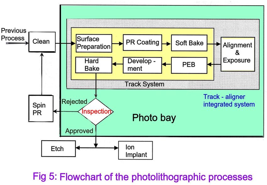
What is a pattern?

➢ The arrangement of black and white areas on
 the mask (glass plate) is called pattern.

➢ The pattern indicates the areas through which
 light will expose the photoresist

                                             9
Requirements of a Photoresist
1. PR should be sensitive to the desired
     frequency and insensitive to yellow or red
     light.
2.   It should have fine line definition that should
     be retained during subsequent processing
     while it is still present on the wafer.
3.   The exposed resist should undergo chemical
     changes
                                                10
Requirements of a Photoresist (contd.)
4. The ‘HARD RESIST’ (chemically inert part of the resist)
should bind strongly to the substrate or the layer below
PR.
5. The ‘SOFT RESIST’ (chemically active part of PR)
should be easily removable from the wafer surface.
6. The Hard PR should be able to sustain further processing
(Etching) without losing fine line definition.
7. The PR must not contribute impurities, introduce defects
or in any other way degrade the performance of 11
the
device being fabricated.Requirements of a photoresist (contd.)
8. The Hard PR should be easily removable when it
is no longer required, without adversely affecting
the other layers present.
- This process of Hard PR removal is called
STRIPPING
- Chemical used for stripping the hard PR is
called ‘STRIPPER’
- ‘Plasma Aching’ is the technique used for
removing hard PR by plasma technique
12PR Components
13Types of photoresist (PR)
Photoresists are of 2 types
1. Positive – it creates a + ve image of
the pattern on the mask.
2. Negative – it creates a – ve image of
the pattern on the mask.
14Two Types of Photoresists
Negative PR and Positive PR
Negative PR
– The exposed parts become cross linked and
polymerized due to the photochemical
reaction, which hardens and remains on the
wafer surface after development, whereas
the unexposed parts are dissolved by the
developer.
1516
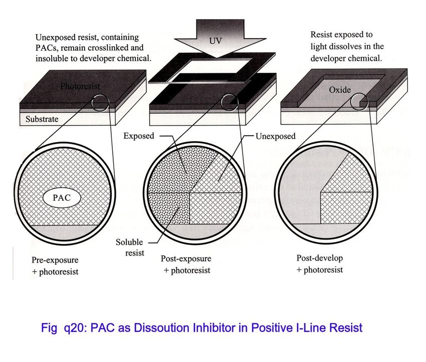
Positive Photoresist
❖ The main component is novolac resin, which is a
 crosslinked polymer before the exposure.

❖After the exposure process, the exposed part’s
 cross-links break down and become “softened” due
 to    the      photochemical     reaction      called
 photosolubilization,

❖It will be dissolved by the developer, while the
                                                  17
 unexposed parts remain on the wafer surface.
Use of Photo Active Compound
18DQN Positive Photoresist
➢ Diazo-Quinone Novalac is a +ve PR
➢ Its Photo-active Compound is Diazo-quinone
➢ Its matrix material is novalac
19Photoresist Parameters (Useful Properties)
➢ Dose – it is the total quantity per unit area of photons
falling on PR.
Dose θ = Photon intensity x Exposure time
Units: Energy (calories or joules) per unit area
➢ Sensitivity – amount of light energy necessary to create the
chemical change
➢ Resolution – Smallest feature size that can be reproduced in
a photoresist.
➢ Contrast – is the difference in appearance of two or
more parts of a field seen simultaneously or
20
successively.21
22
What is a Mask?

A photomask is an opaque plate with holes or

 transparencies that allow light to shine through in a

 defined pattern. They are commonly used in

 photolithography.

                                                  23
Dark Field Mask and Clear Field Mask
➢ Active Region - region of interest
➢ Field Region – rest of the glass plate region
➢ If the field region is dark it is a dark field mask
➢ If the field region is clear , it is a clear field mask
2425
26
Preference between Dark Field Mask and
Clear Field Mask

For aligning mask with the pattern on the wafer

  we must see the wafer pattern through the

  mask. Therefore a clear field mask is

  preferred.

                                              27
Imaging errors due to
dust particles:
error is critical
- if the particle is in Masks without Masks with
dust particles dust particles
active region
- if the mask is dark
field
2829 F 632
Define Function
                           Flow diagram for mask
Partition Design           generation process

High-level Simulation

Assembly/Layout Functional Blocks           Layout rules

Low-level simulation                Device performance
of new blocks                       files

Check for layout rules violation

Generate PG (mask) file             Mask Fabrication
                                                         30
Layout of the Inverter (CMOS)
pMOS
nMOS p- well n-well Source
Drain
Gate
Metal
Contacts
nMOS pMOS
Source Drain
31Layout Showing 8 Invertors
3233
Wafer

        34
Mask 1
pWell
35Mask 2
nWell
36Mask 3
pMOS S & D
37Mask 4
nMOS S & D
38Mask 5
Poly
39Mask 6
Contacts
40Mask 7
Metal Lines
41Mask 8
Metal Lines
42Mask 9
Contact Holes
43Alignment
of Masks
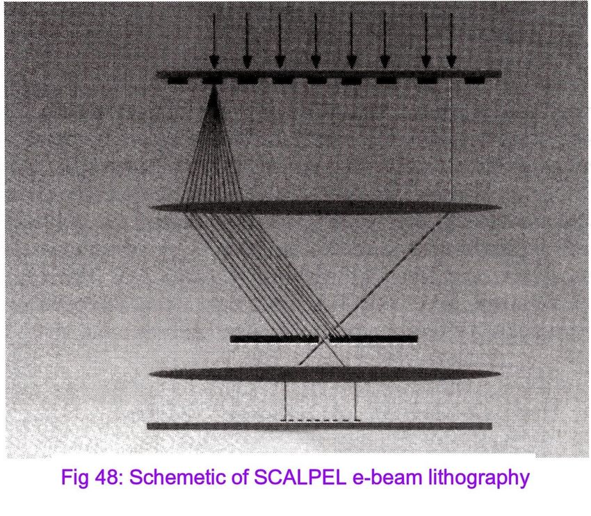
44Electron-Beam Lithography
45Photoresist Parameters (contd. ..)
➢Contrast –is the difference in appearance of two
or more parts of a field seen simultaneously or
successively.
Contrast: = ץ1 / [log10(D100/D0)]
Where D100 = lowest energy density
for which all the resist is removed,
D0 = lowest energy density
needed to begin photo chemistry
46Fraction of resist remaining
D0
1.0
0.8
0.6 Contrast curve
for + ve resist
0.4
0.2 D100
0.0
Exposure Dose (mJ/cm2
47Critical Modulation Transfer Function
(CMTF)
CMTF is the minimum optical modulation transfer
function necessary to obtain a pattern. It is
defined by:
CMTF = (D100 – D0)/(D100 + D0)
4849 F6.47
Alignment Systems
        and
   Misalignments

                    50
Photolithography
Silicon Substrate
SiO2
Insoluble Photoresist
UV light
Glass mask with feature
Exposed Photoresist
51Photolithography (continued)
Chemical Etch or Dry Etch
Hardened
Photoresist
5253
54
55
➢What is PEB ?

➢How it works ?

➢Why is it useful?

                     56
F 6.17
5758
F 619

        59
F 620
60Questions • Explain the working of +ve & -ve PR • Why + PR gets higher resolution • What is resolution? • Two (2) basic techniques for transferring resist features into a layer with proper schematic representation • Working of electron lithography 61
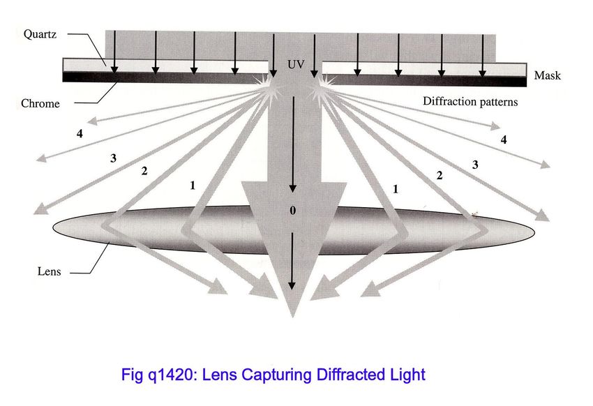
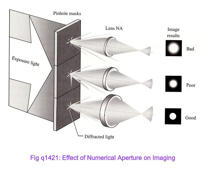
Resolution and Focusing

                          62
q1421 S. K. Bhatnagar 63
64
NA = 2 ro / D
                65
Q 1428
6667
q1429

        68
Q. Can we continue to reduce
wave length to improve resolution?
69q1430
7071
q1431

Focus the light on the mid-plane of PR to optimize resolution
                                                           72
F 6.40 S. K. Bhatnagar 73
F 6.41

         74
F6.42 S. K. Bhatnagar 75
f43

      76
Reducing Wave Length
7778
➢Intensity of DUV sources
F 6.04
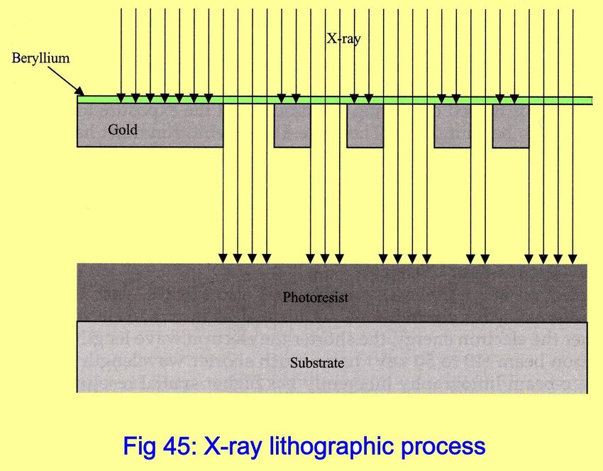
80X-ray Lithography
81X-ray Lithography
➢Wavelength < 5 nm; Higher resolution
➢No materials that can reflect or refract x-rays
➢Must be accomplished by the direct printing
process – similar to proximity printing
82F 6.45
83F 6.46
➢Thin layers of chromium can block UV light
➢Thick layer of gold is required to block X – rays.
Therefore thickness to gap ratio changes.
84Extreme Ultra Violet (EUV) radiation
(11 – 14 nm) for sub-0.1 micron features
➢No known material can be used to make
lenses for EUV – strong absorption at short
wave lengths
➢Therefore EUV systems must be mirror-
based
➢Light sources still under development
➢Material of masks – multilayer coatings such
as Pd/C , Mo/Si
85f44
86Ion-beam Lithography
87Ion-Beam Lithography ➢Similar to e-beam lithography – higher resolution ➢Can be both – direct writing and projection resist exposing ➢Advantage – direct ion implantation and ion-beam sputtering patterned etch ➢Disadvantage – throughput is very low ➢Application – mask/reticle repair 88
F6.48

        89
F 639
9091
92
q1446
F 626

        93
Thank You
94You can also read