Characterisation of dynamic focusing properties using MOEMS system (mes)
←
→
Page content transcription
If your browser does not render page correctly, please read the page content below
Prof. Dr. Ulrich Mescheder
B.1.10
mes@hs-furtwangen.de

Master Thesis topics for summer semester 2021
 (Research Institute for Microsystem Technology, https://www.hs-furtwangen.de/en/research/research-
institutes/institute-for-microsystems-technology/)

Topics related to medical and health care:

I Topics embedded in running research projects
(special conditions and ressources as third party fundings are available, these topics can be linked to
additional assistant jobs, non-disclosure agreements may have to be considered)

1. Characterisation of dynamic focusing properties using MOEMS system (mes)
Within a project an active focusing system for laser scanning system has been developed. The main component
for this purpose is a MOEMS devices developed at HFU using a reflective membrane (micromirror device) which is
electrostatically actuated in such a way that an almost perfect parabolic surface is obtained. The bending of the
surface can be adjusted by the applied voltage (typically up to 200 V). Within a thesis a µC-based electronic control
system has been designed which allows to drive the micromirror device with according control signals provided by
the laser scanning system.

In this thesis, specifically, the dynamic behaviour should be investigated using FEM, given devices and to be built-
up set-ups
     - Understanding of MOEMS device (practical testing)
     - Learning COMSOL multiphysics
     - Modal analysis of device (based on previous models)
     - Test-set-up for dynamic characterisation (optical set-up)
     - Comparison simulation and experiments
     - Modelling of frequency dependence
     - documentation
Literature
U. Mescheder, M. Freudenreich, S. Somogyi, C. Estan: Distortion optimized Focusing Mirror Device with Large
Aperture: Journal: SENSORS AND ACTUATORS A: PHYSICAL Vol. 130-131, 2006, p. 20-27]
W. Kronast, U. Mescheder, B. Müller, R. Huster: Development of a focusing micromirror device with in-plane
stress relief structure in SOI technology. Proc. SPIE 8616, MOEMS and Miniaturized Systems XII, 86160Z
(March 13, 2013), San Francisco, 2013
W. Kronast, U. Mescheder, B. Müller, R. Huster: Entwicklung einer Stressausgleichsstruktur für span-nungsarme
aktive Membranspiegel in SOI Technologie. In: GMM ; VDI/VDE-IT (Hrsg.): MikroSystem-Technik Kongress
2013, 880 Seiten, CD-ROM, ISBN 978-3-8007-3555-6, S. 432-435
W. Kronast, U. Mescheder, B. Müller, R. Huster: Development of a focusing micromirror device with an in-plane
stress relief structure in silicon-on-insulator technology. J. Micro/Nanolith. MEMS MOEMS. 13(1), 011112 (Jan
21, 2014), ISSN 1932-5150, doi:10.1117/1.JMM.13.1.011112, 10 Seiten

For further information, please contact Prof. Ulrich Mescheder (mes@hs-furtwangen.de)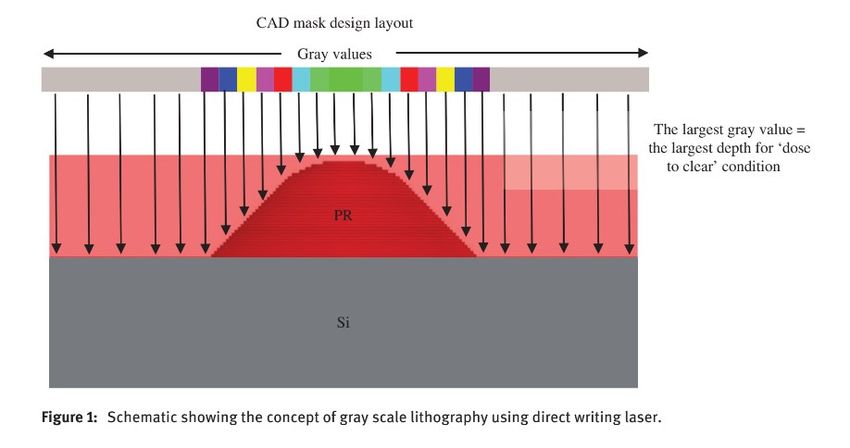
2. Development of a microfluidic platform for cell cultivation with porous Si-
   membranes
Introduction: The understanding of cell to cell interactions is of high interest for many biomedical questions.
Examples are therapeutic interventions resulting from analyzing tumor-stroma interactions or permeability studies
of new CNS pharmaceuticals with the help of in-vitro models of the Blood-Brain-Barrier. To enable analysis of
various cell behaviors, advanced 3D cell cultivation systems in combination with different qualitative and
quantitative analyzation methods are needed and are subject of many research activities. To provide the needed
3D environment for cell cultivation, often chambers separated by permeable membrane structures are used.
At the HFU, there is a long experience on porous Silicon with pores in the nm-range, thus in principle suitable for
such membranes. However, due to the problem of electrolytical short-cut when a pore is etched throughout the
Si, more sophisticated approaches are needed to get defined pores (defined in size and density). E.g. defined
etch stop layers in the bottom in combination with local backside and frontside openings might provide well
defined membranes with nanopores.
Aim of the research: In this project a microfluidic platform must be developed, on which the cell-growth as well
as cell to cell interactions can be characterized. For the permeable membranes, separating different cultivation
chambers, porous Si-membranes are used. The developed microfluidic system must be integrable in other
microfluidic systems with defined interfaces. Main part of the thesis will be the concept development of the
complete system considering the framework conditions of the processes needed to develop self-organized
porous Si-membranes.
Requirements: clean room experience and base knowledge of Si-technology processes, base knowledge in
medical technology and the area of cell cultivation
The project is for preparation of a cooperation project starting at 1st of January 2021, together with two
companies.
Tasks:
     - literature research (focus on cell cultivation systems and manufacturing processes of porous Si-
          membranes)
     - improvement of an existing concept for the microfluidic membrane system
     - flowchart for the manufacturing process of the microfluidic system with porous Si-membranes
     - development of a suitable test-setup for permeability studies of the porous-membrane structures
     - development, manufacturing and characterization of a simplified microfluidic demonstrator setup which
          emulates the basic characteristics of the proposed microfluidic membrane system (e.g. flow through
          porous structures with intermediate cell cultivation space)
Literature:
- R. Booth und H. Kim, Lab Chip 12, p.1784, 2012;
- L. Griep et al., Biomed Microdevices 15, p.145, 2013;
- B. Prabhakarpandian et al., Lab Chip 13, p.1093, 2013;
- H. Becker ,Applications of organs‘ on-a-chip,IVAM µFludik-Workshop, 8.3.2018, Dortmund
- C.L. Haynes, R.P. Van Duynes, A versatile Nanofabrication Tool for studies of size dependent
  Nanoparticle Optics, The Journ. Of Phys. Chemistry, B105, pp. 5599-6511, 2001
- R. Booth und H. Kim, „Permeability Analysis of Neuroactive Drugs Through a Dynamic Microfluidic In
  Vitro Blood–Brain Barrier Model,“ Ann Biomed Eng, Bd. 42, pp. 2379-2391, 2014.
- Kovacs, A., Kovacs, A., Pogany, M., Mescheder, U. (2007) “Mechanical investigation of perforated
  and porous membranes for micro- and nanofilter applications.” Sensors and Actuators B: Chemical
  127(1): 120-125
- Kovacs, A., Kovacs A., Mescheder U., (2008) “Estimation of elasticity modulus and fracture strength
  of thin perforated SiN membranes with finite element simulations.” Computational Material
  Science 43: 59-64
- Kentaro Kawai, „Nanopore Formation to Thin SiO2 Membrane in Electrolyte Solution Using
  Dielectric Breakdown“, Proceedings 30th Eurosensors, September 2016, Budapest).
- Kwok, H., Briggs, K., Tabard-Cossa V (2014) “Nanopore Fabrication by Controlled Dielectric
  Breakdown.” PLoS ONE 9(3)
- Zifan Tang, Daihua Zhang, Weiwei Cui, Hao Zhang, Wei Pang and Xuexin Duan (2016) “Fabrications,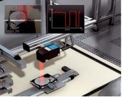
Applications and Challenges of Solid-state Nanopores: A Mini Review.” Nanomater Nanotechnol, 6:
  35
- Velleman, L et al. Fabrication of self-supporting porous silicon membranes and tuning transport
  properties by surface functionalization, Nanoscale, 2010, 2, 1756–1761
- Venkatesan, B. M., Dorvel, B., Yemenicioglu, S., Watkins, N., Petrov, I., & Bashir, R. “Highly Sensitive,
  Mechanically Stable Nanopore Sensors for DNA Analysis.” Advanced Materials 21(27): 2771–2776,
  (2009)
- Venkatesan BM, Bashir R. “Nanopore sensors for nucleic acid analysis.” Nat Nano 6, 615–624,
  (2011)
For further information, please contact Prof. Ulrich Mescheder (mes@hs-furtwangen.de) or M.Sc. Benjamin
Sittkus (siku@hs-furtwangen.de)

3. Forceless sensor system for finger position detection in Braille reader systems
   (MED) (mes)
Braille displays (fig. 1 [1]) are important tools to help blind or visually handicapped people to read and write data.
In this project a new concept for sensing the finger position, to identify the “reading finger” (to control “cursor”
setting during reading) has to be investigated.
In a first stage different contact- and forceless methods such as PCAP or PCT [2] have to investigated
theoretically and compared in respect to the specific needs in a Braille display using COMSO mulitphysics.
. PCAP is widely used for touch displays in mobile phones or pads and are based on capacitance change due to
a finger tip nearby (fig.2).
For a “test kit” [3] hardware on flexible substrate should be developed.
Especially, the principle physical sensing effects used in (commercial) devices have to be considered for a proper
selection of suitable principles used here. Specifically designed sensing structures can be realized in
theTechnology lab for micro- and nansosystems.
For a selected method, a first test set-up should be realized and sensor data should be analyzed.

This project is part of a cooperation with the company Helptech, Horb (Germany).

Tasks:
     - Literature research about touch displays (principles, set-ups, materials, pros/cons
     - Building a model in COMSOL multiphysics, modelling of expected output signals
     - Design of PCAP for Braille display (concept for realization below polymer surface)
     - Design and microfabrication of specific structures fortest set-up (shadow mask)
     - Construction of test set-up and characterization
     - Documentation and presentation
Literature:
[1] https://helptech.de/en/products/braille-displays-and-note-takers/braille-keyboards
[2] https://www.hy-line.de/infothek/veroeffentlichungen/whitepapers-fachartikel/hcc-fachartikel/ein-klassiker-
erfindet-sich-neu/
[3] Narjes Pourjafarian , Anusha Withana , Joseph A. Paradiso , Jürgen Steimle, Multi-Touch Kit: A Do-It-Yourself
Technique for Capacitive Multi-Touch Sensing Using a Commodity Microcontroller, UIST ’19, October 20-23,
2019, New Orleans, LA, USA. Copyright is held by the author/owner(s). ACM ISBN 978-1-4503-6816-2/19/10.
http://dx.doi.org/10.1145/3332165.3347895

Literature:
[1] https://helptech.de/en/products/braille-displays-and-note-takers/braille-keyboards
[2]         https://www.hy-line.de/infothek/veroeffentlichungen/whitepapers-fachartikel/hcc-fachartikel/ein-klassiker-
erfindet-sich-neu/
[3] Narjes Pourjafarian , Anusha Withana , Joseph A. Paradiso , Jürgen Steimle, Multi-Touch Kit: A Do-It-Yourself
Technique for Capacitive Multi-Touch Sensing Using a Commodity Microcontroller, UIST ’19, October 20-23,
2019, New Orleans, LA, USA. Copyright is held by the author/owner(s). ACM ISBN 978-1-4503-6816-2/19/10.
http://dx.doi.org/10.1145/3332165.3347895

For further information, please contact Prof. Ulrich Mescheder (mes@hs-furtwangen.de)
II Topics for dissimilation and exploitation of developments
4. Characterization and exploitation of a micromechanical laser scanning system
Within a cooperative project (Prof. Kallmann, Prof Mescheder) a laser projection system has developed which
is based on a micromechanical, electrostatically actuated cylinder lens which allows to adjust the beam width
of a laser beam within laser projection systems (e.g. in a profilometer). An experimental set-up and the
micromechanical components have been developed and are available for testing.
Within the project, the system should be evaluated experimentally (detailed characterisation of performance
and properties). The developed models (COMSOL, FEM) should be adjusted in respect to the experimental
results. A demonstrator showing the use of the device for laser scanning systems should be built up.
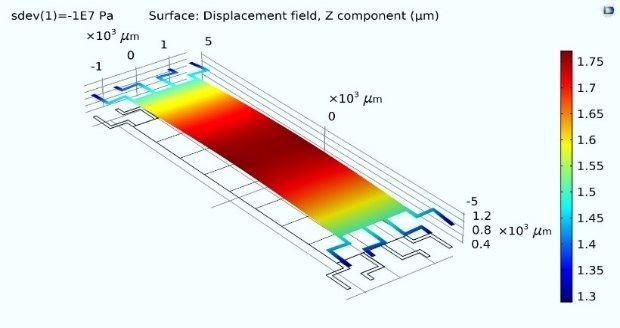
Fig.: Top left: simulated bending of the m icromechanical, cylinder shaped membrane, top right: principle of
laser beam adjustment, bottom left: Profilometer, Sick AG, bottom right: microscopic picture of fabricated
micromechanical device
Tasks:
Literature Study
Experimental characterization (mechanical, optical and dynamical properties)
analysis of the data and evaluation of different membrane suspensions regarding buckling and parabolic
deformation
Optimisation of FEM-models
Concept of laser scanning system
Building up laser scanning system
characterization
Documentation
Contact and further information: (Ulrich Mescheder, mes@hs-furtwangen.de)
Literature:
W. Kronast, U. Mescheder, B. Müller, R. Huster: Development of a focusing micromirror device with an in-plane
stress relief structure in silicon-on-insulator technology. J. Micro/Nanolith. MEMS MOEMS. 13(1), 011112 (Jan
21, 2014), ISSN 1932-5150, doi:10.1117/1.JMM.13.1.011112, 10 SeitenSchenk, H.; Dürr, P.; Haase, T.; Kunze, D.; Sobe, U.; Lakner, H.; Kück, H.
Large deflection micromechanical scanning mirrors for linear scans and pattern generation, IEEE Journal of
Selected Topics in Quantum Electronics 6 (2000), Nr.5, S.715-722
Mostafa Abdel-Bary Ebrahim, 3D LASER SCANNERS: HISTORY, APPLICATIONS, AND FUTURE Review
Article (2011), DOI: 10.13140/2.1.3331.3284 Available from:
https://www.researchgate.net/publication/267037683_3D_LASER_SCANNERS_HISTORY_APPLICATIONS_AN
D_FUTURE?channel=doi&linkId=5442bdf10cf2e6f0c0f93727&showFulltext=true [accessed Jun 07 2020].
II Other thesis topics
The following thesis topics are innovative and related to fundamental research questions. Thus, these projects
might be continued as PhD topics.
5. Grayscale lithography for fabrication of 3D structures using negative photoresist with direct writing
laser (DWL 66FS) device (
Negative resist?
Direct writing laser enables the maskless exposure of the CAD layout design on the wafers coated with photoresists.
The laser intensity of the DWL device can be modulated to expose the photoresist with variable depth of exposures;
thereby, enabling the grayscale exposure (3D) of the photoresists. This technique has been successfully
investigated in case of positive photoresists (i.e. the exposed regions are dissolved in developer), however it is still
vaguely investigated in case of negative photoresists (i.e. the exposed regions remain during the development).
Therefore, in this thesis work, the applicability and feasibility of grayscale exposure of negative photoresist has to
be investigated.
Schematic of grayscale lithography in case of positive photoresist, in case of negative photoresist the reversed is
expected, the exposed region would remain during development and the unexposed photoresist would dissolve,
so a microchannel is expected in the dark red region in the above schematic.
The tasks involved in the thesis work:
1. Literature study involving the grayscale lithography especially those with negative photoresists.
2. Training with the Heidelberg Instruments DWL66FS device (direct writing lithography device)
3. Selection of the negative photoresists
4. Design of the CAD layout
5. Test exposures and development
6. Characterization of the exposed photoresists
7. Documentation
Literature:
[1] F. Lima, I. Khazi, U. Mescheder, A. Tungal, U. Muthaih: Fabrication of 3D microstructures using grayscale
lithography, Advanced Optical Technologies: vol:8, iss:3, 2019 (in Press)
[2] Isman Khazi, Ulrich Mescheder, Uma Muthaih: 3D free forms in c-Si via grayscale lithography and RIE,Microelectronic Engineering Volume 193, 5 June 2018, Pages 34-40 [3] Uma Muthiah, Isman Khazi, Ulrich Mescheder: 3D Structuring of Silicon using Grayscale Technology, Proceedings Mikrosystemtechnik Kongress, Munich 2017 [4] F. Lima, A. Tungal, I. Khazi, U. Mescheder: Galvanisch aus 3D-Fotolack-Strukturen abgeformte metallische 3DFreiformen, Proceedings Mikrosystemtechnik Kongress, Munich 2017 Contact: Isman Khazi (kmi@hs-furtwangen.de) and Prof. Dr. Mescheder (mes@hs-furtwangen.de)
You can also read