Crypto-Core Design using Camellia Cipher
←
→
Page content transcription
If your browser does not render page correctly, please read the page content below

Journal of Physics: Conference Series

PAPER • OPEN ACCESS

Crypto-Core Design using Camellia Cipher
To cite this article: Chew Wei Ci et al 2021 J. Phys.: Conf. Ser. 1755 012019

View the article online for updates and enhancements.

                               This content was downloaded from IP address 46.4.80.155 on 27/04/2021 at 15:39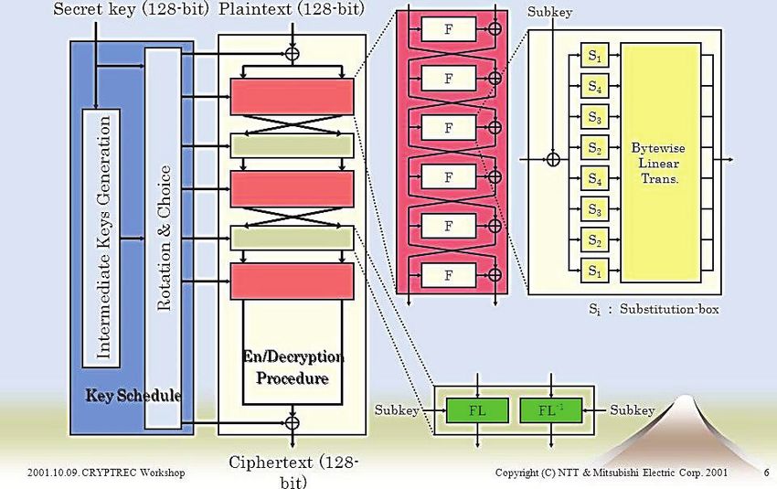
5th International Conference on Electronic Design (ICED) 2020                                                   IOP Publishing
Journal of Physics: Conference Series             1755 (2021) 012019                      doi:10.1088/1742-6596/1755/1/012019

 Crypto-Core Design using Camellia Cipher

                      Chew Wei Ci1, Siti Zarina Md Naziri1, Rizalafande Che Ismail1,2, Razaidi
                      Hussin1, Mohd Nazrin Md Isa1 and Muhammad Sufyan Safwan Mohamad
                      Basir3
                      1
                       School of Microelectronic Engineering, Universiti Malaysia Perlis, Perlis, Malaysia
                      2
                        School of Computing and Informatics, Albukhary International University, Kedah,
                      Malaysia
                      3
                       Department of Electrical Engineering, Politeknik Mukah, Sarawak, Malaysia.

                      weicichew85@gmail.com, sitizarina@unimap.edu.my

                      Abstract. Camellia cipher is another symmetric block cipher which allows the encryption and
                      decryption process to share the same key. The cipher permits a 128-bits input data with three
                      different key size: 128, 192 and 256 bits. This paper presents two hardware design approach of
                      Camellia cipher, which are FPGA and custom-based design approach. These approaches
                      utilized design softwares of Altera Quartus II with device family of Cyclone II and Synopsys
                      Design Compiler. The performance of Camellia crypto-core design is then been evaluated
                      based on the implementation platform in terms of speed, area and power. With an equal base
                      of 50MHz of clock frequency, custom-based design is found more efficient than FPGA-based
                      design due to the execution time achieved with 8.46ns, which is faster than the latter that
                      consumed double the time with 16.075ns. The custom-based design achieved 15.13 Gbps of
                      throughput. Besides, the power consumption of custom-based design is 1.3519 mW which is
                      lower than the FPGA-based design. In a nutshell, the design has successfully done as it achieved
                      expected encryption and decryption outcomes with acceptable performance.

 1. Introduction
 Camellia cipher is assessed as one of the secured encryption algorithms that has excellent security and
 performance. Thus, it is suitable for networking security system as it difficult to break. The cipher was
 jointly developed by Nippon Telegraph and Telephone Corporation (NTT) and Mitsubishi Electric
 Corporation in 2000. The cipher provides similar interface specification as AES [1]. Camellia emerged
 as the first Japanese encryption algorithm and it is the block cipher that is recommended by
 CRYPTREC in 2002. Then, it was suggested in the New European Schemes for Signature, Integrity,
 and Encryption (NESSIE) block cipher portfolio in 2003 and finally embraced as a new international
 standard by ISO/IEC in 2005 [2].
     Camellia is another Feistel-based cipher with 18 or 24 rounds depending to the key used. The self-
 styled FL-function (a logical transformation layer) or its inverse, is applied for every six rounds. The
 cipher embeds four 8×8-bit S-boxes comprised of input and output affine transformations and logical
 operations. The input and output key whitening are also used in this cipher.
     Camellia is known to be effectively functional in multiple platforms. The cipher is one of the
 algorithms that can operate on software and hardware implementation efficiently. For example,

              Content from this work may be used under the terms of the Creative Commons Attribution 3.0 licence. Any further distribution
              of this work must maintain attribution to the author(s) and the title of the work, journal citation and DOI.
Published under licence by IOP Publishing Ltd                          1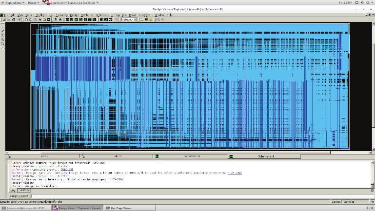
5th International Conference on Electronic Design (ICED) 2020                                IOP Publishing
Journal of Physics: Conference Series             1755 (2021) 012019   doi:10.1088/1742-6596/1755/1/012019

Camellia cipher is able to perform well in compute number of gates for hardware design and implement
smart card system with memory requirement [3].
    Other than that, the cipher provides high level of security. Camellia cipher builds up the protection
wall by using the technique which is known as “state-of-art cryptanalytic”. Therefore, the cipher is
able to be against the advanced cryptanalytic attacks, for instance higher order differential attacks,
boomerang attack etc [3].
    The performance of Camellia in terms of throughput performance is at par with Advanced
Encryption Standard (AES) as mentioned in [4]. Besides, it is comparable to the AES in terms of
security levels and processing capabilities, besides shows better performance in low capacity memory
or compact hardware such as IC cards. Using pipeline architecture, Camellia gains the finest throughput
compared to other architectures in FPGA and ASIC platforms [5][6][7].
    In this paper, Camellia cipher has been designed for crypto-core using two implementation
approach: FPGA and custom-based design. Therefore, further sections will describe on the concept of
Camellia cipher, the methods and software used in realizing the design, the outcomes achieved by each
design approach and finally the analysis of both approaches. This include the comparison work
between these two methods, which highlights the best implementation for this crypto-core.

2. Elements of Camilla Cipher
Camellia cipher with 128-bits key is built of four important elements as shown in Figure 1. All the
elements have their own function in order to complete the encryption and decryption process. The key
schedule in 128-bits is used to encrypt or decrypt the input signal which is the plaintext or cipher text
in 128-bit length. During the encryption or decryption process, the F-function block and the FL-
function will take place where the S-boxes function block plays its role in F-function block. The S-
boxes in Camellia are alike the structure of AES's S-box. Camellia permits three different key sizes
which is 128, 192 and 256 bits [4].
    Classical Feistel network is a structured feature in Camellia cipher which provides special operation
after each six Feistel rounds. These operations bring benefit in complicating certain attacks, however
the classical Feistel structure will blemish. Hence, Camellia cipher operates in a range of 18 (for 128-
bit key) to 24 rounds (for 192- and 256-bit key) due to the classical Feistel Network is plugged in after
every six rounds of Feistel [4].

                           Figure 1. Architecture of Camellia block cipher [4].

                                                      2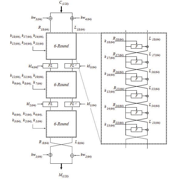
5th International Conference on Electronic Design (ICED) 2020                                IOP Publishing
Journal of Physics: Conference Series             1755 (2021) 012019   doi:10.1088/1742-6596/1755/1/012019

2.1. Encryption
The encryption procedure for 128-bit key is shown in Figure 2 which involve the following step, with
!" as the sub keys:

                                        #$ % &$ = ' ( )!"* % !"+ ,

                             Figure 2. The architecture of encryption process.

Explanation: the plaintext -)*+., is XORed with !"*)/0, % !"+)/0, and separated into #$)/0, % &$)/0,
of equal length, for example:

                            -)*+., ( 1!"*)/0, % !"+)/0, 2 = #$)/0, % &$)/0,

Then, the following operation is performed from 3 = 4 to48, expect for 3 = 6 and 45.

                                         #7 = &79* :;)#79* < !7 ,!
                                         &7 = #79* >

where for 3 = 6 and45, the following is carried out:

                                        #? 7 = &79* :;)#79* < !7 ,!
                                        & ? 7 = #79* !
                                        #7 = ;# @#? 7 < !A +7 B!
                                                          /9*

                                                      3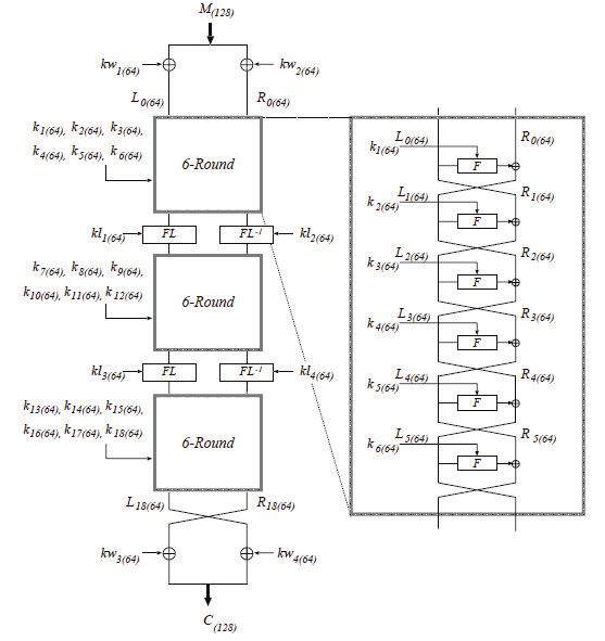
5th International Conference on Electronic Design (ICED) 2020                                IOP Publishing
Journal of Physics: Conference Series             1755 (2021) 012019   doi:10.1088/1742-6596/1755/1/012019

                                        &7 = ;#9* )&? 7 < !A+7 ,
                                                             /

&*.)/0, And #*.)/0, are concatenated and XORed with!"C)/0, % !"0)/0, . The resultant value is the
cipher text. For example:

                              -)*+., = )&*.)/0, % #*.)/0, , ( )!"* % !"+ ,

2.2. Decryption
Figure 3 shows the decryption procedure for 128-bit keys, it just reversing the order of sub keys from
the encryption process. The steps are as follows:

The cipher text D)*+., is XORed with !"C)/0, % !"0)/0, and separated into &*.)/0, % #*.)/0, of equal
length, for example:

                           D)*+., ( 1!"C)/0, % !"0)/0, 2 = &*.)/0, % #*.)/0,

                             Figure 3. The architecture of decryption process.

Then, the following operation is performed from 3 = 48 down to4, expect for 3 = 4E and>F.

                                         #7 = &79* :;)#79* < !7 ,!
                                         &7 = #79* >

                                                      4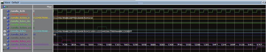
5th International Conference on Electronic Design (ICED) 2020                                 IOP Publishing
Journal of Physics: Conference Series             1755 (2021) 012019    doi:10.1088/1742-6596/1755/1/012019

where for 3 = 4E and F, the following is carried out:

                                     & ? 79* = #7 :;)&7 < !7 ,
                                     #? 79* = &7 !
                                      &79* = ;# G&? 79* < !A+)79*, H!
                                                                 /

                                      #79* = ;#9* G#? 79* < !A)+79*, H
                                                                 /9*

#$)/0, And &$)/0, are concatenated and XORed with !"*)/0, % !"+)/0, . The resultant value is the
plaintext. For example:

                        -)*+., = )#$)/0, % &$)/0, , ( 1!"*)/0, % !"+)/0, 2.

3. Methodology
As to successfully design a Camellia-based crypto-core, the steps in Figure 4 are conducted. Firstly,
the concept of Camellia cipher needs to be studied in order to organize proper design strategies and
approach. Inputs are taken from previous research and technical papers.

                                      Figure 4. Overall design flow.

                                                      5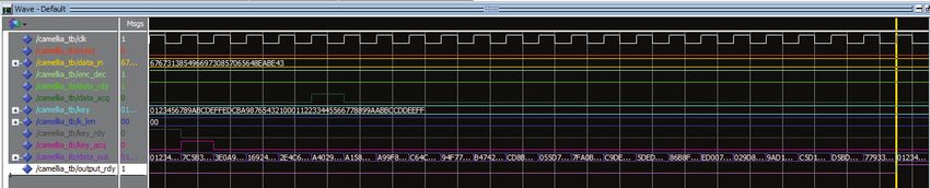
5th International Conference on Electronic Design (ICED) 2020                                 IOP Publishing
Journal of Physics: Conference Series             1755 (2021) 012019    doi:10.1088/1742-6596/1755/1/012019

   Next, the code is written in VHDL in Altera Quartus II [9] environment, where the functionality of
the code is been verified using proper written testbench which includes plaintext. For encryption
process, the plaintext is the input data where the output of the process (known as the ciphertext) will
be the input for decryption process using a specific key. The details of the input and output signals
used in the crypto-core design are listed in Table 1. The generated the output waveform is used to
validate the design.
   Finally, after the design is functionally verified, the summary report of design, timing analysis and
power analysis are generated by Altera Quartus II software which enables the collection of speed, area
and power usage values.

                                 Table 1. Signal description of the design.

      Input/output     Signal in Design            Value                       Description
                              clk              Rising edge                        Clock
                                                     0                             Set
                              reset
                                                     1                            Reset
                            data_in            128-bit data                     Input data
                                                     0                     Encryption process
                            enc_dec
                                                     1                     Decryption process
                                                     0                           Data is
          Input            data_rdy
                                                     1                   Data is ready to process
                              key              256-bit data                     Password
                                                    00                     128-bits key length
                           k_length                 01                     192-bits key length
                                                    10                     256-bits key length
                                                     0             Password is unready to process
                            key_rdy
                                                     1                 Password is ready to process
                            data_out           128-bit data        128-bit cipher text or plain text
         Output                                      0                 Output data still in progress
                          output_rdy
                                                     1                     Output data is ready

   Meanwhile, the custom-based approach utilized the Synopsys Design Compiler [10] software. The
software allows the design to be compiled and synthesized it into actual logics gates by providing
certain constraints. The custom-based process flow is portrayed as Figure 5. Clock frequency, delay
time and minimum area are the constraints of the design.

                                                      6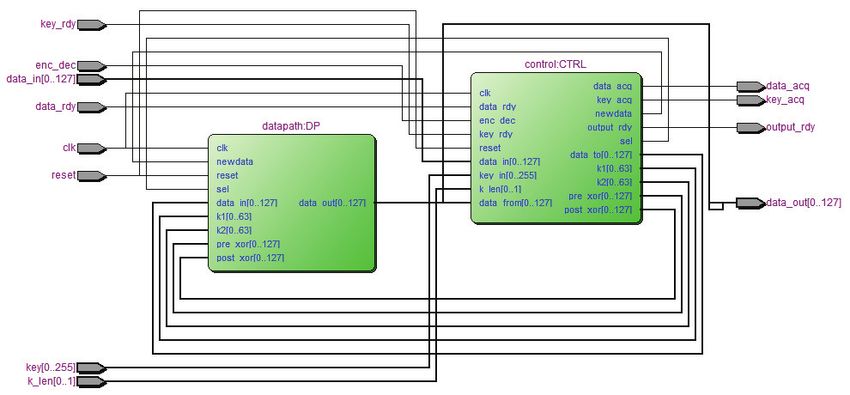
5th International Conference on Electronic Design (ICED) 2020                                IOP Publishing
Journal of Physics: Conference Series             1755 (2021) 012019   doi:10.1088/1742-6596/1755/1/012019

                        Figure 5. Design flow using Synopsys Design Compiler.

4. Result

4.1. FPGA-based Design Results
Once the compilation is done, the testbench file is generated in order to acquire the input and output
waveform. In this design, the encryption and decryption process shared the same key where the key is
set to 128 bits. The correct cipher text is created only when the output_rdy is “1”.
    Figure 6 shows the output waveform for encryption process. The input data is inserted as
“0123456789ABCDEFFEDCBA9876543210”                       where       the       output     data      is
“67673138549669730857065648EABE43”.

               Figure 6. The output waveform of Camellia cipher for encryption process.

   For the decryption process, the input data had used the output data of encryption process previously.
The purpose of this action is to check whether both of the process run properly. Figure 7 shown that
the output result of decryption is the same as the input data for encryption process.

                                                      7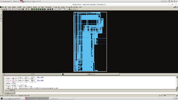
5th International Conference on Electronic Design (ICED) 2020                                  IOP Publishing
Journal of Physics: Conference Series             1755 (2021) 012019     doi:10.1088/1742-6596/1755/1/012019

               Figure 7. The output waveform of Camellia cipher for decryption process.

    After the simulation process, the report of each simulation are generated. Firstly, the analysis and
synthesis summary will pop-out automatically after the compilation. For a detailed view of physical
consumption, the Fitter report is referred which is modelled after the synthesis process. Based on the
Fitter report, it can be observed that the total logic element used are 7,626 (11%) which include 7,337
(11%) of combinational functions and 1,479 (2%) number of registers out of 68,416 of logic elements
offered by the EP2C70F896C6 Altera Cyclone II FPGA. On the other hand, the total pins that has been
used in this project is 522 out of 622, which portrays an 84% usage of pin offered by the device.
    This is followed by the timing analysis in Altera Quartus II with the clock frequency is set to
50MHz. The report shows that the data required time for the design is 22.912ns whereas the data arrival
time is 16.075ns. Meanwhile, the power consumed by the design throughout the simulation is gained
from the Power Consumption summary report. By observation, the total power usage is 255.99mW.
The detailed observation of the design implementation is summarized in Table 2.

                   Table 2. Implementation summary using Altera Cyclone II FPGA

                    Device                                      EP2C70F896C6
                    Frequency                                          50Mhz
                    Total logic elements                                7,626
                    Total combinational functions                       7,337
                    Total registers                                     1,479
                    Total pins                                           522
                    Data required time                                 22.912ns
                    Data arrival time                                  16.075ns
                    Total power usage                              255.99mW

   Finally, the RTL view is generated and shown in Figure 8. It can be clearly seen that the RTL
diagram of Camellia crypto-core is built of two function blocks, which are datapath and control blocks.

                                                      8
5th International Conference on Electronic Design (ICED) 2020 IOP Publishing
Journal of Physics: Conference Series 1755 (2021) 012019 doi:10.1088/1742-6596/1755/1/012019
Figure 8. RTL viewer
4.2. Custom-based Design Results
As for a fair comparison, the design was synthesized using Synopsys Design Compiler based on the
same clock frequency of 50MHz as used in FPGA implementation. Figure 9 shows the original
schematic diagram which before any constraint is applied. It can be observed that the arrangement of
the area of schematic is massive and not fully optimized. After given appropriate constraint of clock
and area, the schematic diagram emerged into another fine form as shown in Figure 10.
Figure 9. Schematic diagram before constraint.
95th International Conference on Electronic Design (ICED) 2020 IOP Publishing
Journal of Physics: Conference Series 1755 (2021) 012019 doi:10.1088/1742-6596/1755/1/012019
Figure 10. Schematic diagram after constraint of clock frequency 50MHz.
Referring to Figure 11(a), the total area consumption is 34,620 µm2 after optimization. A total of
27,449 µm2 of area are spent for the design. In terms of total cells used, the design utilized 11,025 of
unit cells while the total number of register nets are 11,419. Meanwhile, the power consumption of the
crypto-core design after constraint is around 1.3519mW as mentioned in Figure 11(b).
(a) Area report (b) Power report
(c) Timing report
Figure 11. Synthesis reports from Synopsys Design Compiler (Clock frequency = 50 MHz)
105th International Conference on Electronic Design (ICED) 2020 IOP Publishing
Journal of Physics: Conference Series 1755 (2021) 012019 doi:10.1088/1742-6596/1755/1/012019
Instead of area and power consumption, the software also generates the timing report as shown in
Figure 11(c). The design needs 18.65ns to complete the process and the data arrival time is 8.46ns.
This marks the design frequency to 118.2MHz. Meanwhile, the slack obtained is in positive value
which is 10.19 ns. This means that the design met the requirement margin.
5. Discussion
Based on the results generated from both design implementation, the outcomes were than compared
and analyzed. Table 3 shows the result comparison for FPGA-based and custom-based design using
the same clock frequency of 50MHz.
In a nutshell, based to the data have been recorded, it can be concluded that the custom-based design
is more efficient compared to FPGA-based design with the same frequency of 50MHz. This
phenomenon is proven by Table 3, as the number of the registers in custom-based design is 11,419
which is more than the number of the register utilized in FPGA-based. This is because the faster the
speed of the system, the large number of registers being used. Besides, the most significant difference
between FPGA-based and custom-based design is the power consumption of the simulation. Referring
to the same table, the power consumption of FPGA-based design is extremely higher compared to
custom-based design.
Table 3. Result comparison for FPGA-based and custom-based design on 50 MHz of
clock frequency
Number of Total Power Clock Total Time
Registers Consumption Frequency Taken
FPGA-based 1,479 255.99 mW 50 MHz 16.075 ns
Custom-based 11,419 1.3519 mW 50 MHz 8.46 ns
On the other hand, Table 4 portrays the comparison of this work with previous Camellia designs in
terms of device, technology and throughput achieved. To note, throughput, as important speed indicator
for any encryption design, is observed as the total plaintext in bytes or bits encrypted/decrypted divided
by the encryption/decryption time. It is found that the throughput of this design is in the acceptable
range as compared to other designs. The achievement may vary as the approach and technique of each
design are unique and aimed for specific reason and application. Higher throughput marks better time
consumption for encryption/decryption for the design, however, may suffer the area consumption as
the result of excessive usage of registers, especially for using fully pipeline as in [8].
Table 4. Result comparison of this work with other Camellia designs
Chip/ASIC Technology Throughput
Čiča [8] Xilinx Virtex5 XC5FX70T-1FF1136 32.15 Gbps
Denning et al. [11] Xilinx Virtex-II pro XC2Vp50 33.25 Gbps
Nishikawa et al. [12] Tesla C2050 50.6 Gbps
Xilinx Spartan-S XC3S50-5 32.96 Mbps
Kavun & Yalcin [5]
0.13-μm CMOS 81 Mbps
115th International Conference on Electronic Design (ICED) 2020 IOP Publishing
Journal of Physics: Conference Series 1755 (2021) 012019 doi:10.1088/1742-6596/1755/1/012019
Chip/ASIC Technology Throughput
Xilinx Virtex-E v1000efg860 135 Mbps
Cheng & Heys [13]
0.18-um CMOS 143 Mbps
Altera Cyclone II EP2C70F896C6 8 Gbps
This work
0.13-μm CMOS 15.13 Gbps
6. Conclusion
In this paper, a crypto-core was designed using the Japan’s very own encryption algorithm i.e. Camellia
cipher. The design was implemented in two approach, FPGA and custom-based approach. The result
for both approaches is obtained and compared in order to observe the significant difference. Altera
Quartus II provides user friendly functions and easier to get sources from online platform. In Altera
Quartus II 13.0 version, the waveforms can be generated using created testbench and compiled directly
for simulation. Besides, this software compiled the code in short duration.
Meanwhile, the custom-based design approach provides more detail and specific summary report
for total area, time, and power consumption of the design. The Synopsys Design Compiler, enables the
usage trials of different clock frequency and produced custom achievement of performance parameters
which include delay time, number of registers being used, total area as well as schematic diagram after
constraints were given. However, the FPGA design approach allows the rapid hardware
implementation and result as the design can be downloaded into the hardware (i.e. FPGA) to view the
actual result.
The result is of both implementation approaches are then been compared. It can be observed that
the power usage and the execution time in FPGA-based design is higher than the custom-based
approach. Based on the successful functional verification done previously in both platforms, the crypto-
core design has been successfully designed and functioned. The design also has achieved acceptable
value of throughput as compared to other Camellia design.
7. References
[1] L. Xiao and H. M. Heys, “A simple power analysis attack against the key schedule of the
Camellia block cipher,” vol. 95, Issue 3, pp. 409–412, 2005.
https://doi.org/10.1016/j.ipl.2005.03.013.
[2] Y. Liu, D. Gu, Z. Liu, and W. Li, “The Journal of Systems and Software Improved results on
impossible differential cryptanalysis of reduced-round Camellia-192/256,” Journal of Systems
and Software, vol. 85, no. 11, pp. 2451–2458, 2012, doi: 10.1016/j.jss.2012.05.051.
[3] K. Aoki, T. Ichikawa, and M. Kanda, “Camellia : A 128-Bit Block Cipher Suitable for Multiple
Platforms — Design and Analysis,” In: Stinson D.R., Tavares S. (eds) Selected Areas in
Cryptography. SAC 2000, Lecture Notes in Computer Science, vol 2012, pp. 39-56, Springer,
Berlin, Heidelberg, 2001.
[4] L. R. Knudsen, “Analysis of Camellia,” a contribution for ISO/IEC JTCI SC27,
http://info.isl.ntt.co.jp/camellia/Publications/knudsen.ps pp. 1–18, 2000.
[5] E. B. Kavun and T. Yalcin, "A pipelined camellia architecture for compact hardware
implementation," ASAP 2010 - 21st IEEE International Conference on Application-specific
Systems, Architectures and Processors, Rennes, 2010, pp. 305-308, doi:
10.1109/ASAP.2010.5540987.
[6] M. Rogawski. “Analysis of Implementation Hierocrypt-3 algorithm (and its comparison to
Camellia algorithm) using ALTERA devices.” IACR Cryptol. ePrint Arch. 2003 (2003): 258.F.
Q. Ii et al., “Quartus II Introduction Using VHDL Designs,” Program, no. May, pp. 1–36, 2011.
125th International Conference on Electronic Design (ICED) 2020 IOP Publishing
Journal of Physics: Conference Series 1755 (2021) 012019 doi:10.1088/1742-6596/1755/1/012019
[7] P. Yalla and J. Kaps, "Compact FPGA implementation of Camellia," 2009 International
Conference on Field Programmable Logic and Applications, Prague, 2009, pp. 658-661, doi:
10.1109/FPL.2009.5272349.
[8] Z. Čiča, "Pipelined implementation of Camellia encryption algorithm," 2016 24th
Telecommunications Forum (TELFOR), Belgrade, 2016, pp. 1-4, doi:
10.1109/TELFOR.2016.7818785.
[9] Altera, “Introduction to the Quartus II Software,” pp. 1–10, 2011.
[10] Synopsys, “Design Compiler Use Guide,” no. September, 2013.
[11] D. Denning, J. Irvine and M. Devlin, "A high throughput FPGA Camellia implementation,"
Research in Microelectronics and Electronics, 2005 PhD, Lausanne, Switzerland, 2005, pp. 137-
140 vol.1, doi: 10.1109/RME.2005.1543022.
[12] N. Nishikawa, K. Iwai and T. Kurokawa, "High-Performance Symmetric Block Ciphers on
CUDA," 2011 Second International Conference on Networking and Computing, Osaka, 2011,
pp. 221-227, doi: 10.1109/ICNC.2011.40.
[13] H. Cheng and H. M. Heys, "Compact Hardware Implementation of the Block Cipher Camellia
with Concurrent Error Detection," 2007 Canadian Conference on Electrical and Computer
Engineering, Vancouver, BC, 2007, pp. 1129-1132, doi: 10.1109/CCECE.2007.287.
13You can also read