CSE 2021 Computer Organization - AAppppeennddiixx CC The Basics of Logic Design
←
→
Page content transcription
If your browser does not render page correctly, please read the page content below
CSE 2021 Computer Organization

   Appendix C

   The Basics of Logic Design
Outline
n Fundamental Boolean operations
n Deriving logic expressions from truth
tables
n Boolean Identities
n Simplifying logic expressions using
Boolean identities
n Combinational and sequential circuits
n Verilog basics
2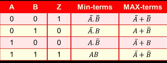
Boolean Algebra
n Boolean algebra is the basic math used
in digital circuits and computers.
n A Boolean variable takes on only 2
values: {0,1} , {T,F}, {Yes, No}, etc.
n There are 3 fundamental Boolean
operations:
n AND, OR, NOT
3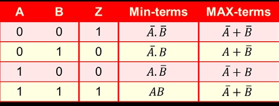
Fundamental Boolean Operations
          AND                    OR                  NOT
  A
                    Z   A                 Z   A                 Z
  B                     B

      Z=A*B (AB)                Z=A+B                  Z=Ā

      Truth Table           Truth Table           Truth Table
      A   B     Z           A    B    Z
                                                   A     Z
      0   0     0           0    0    0
                                                   0     1
      0   1     0           0    1    1
                                                   1     0
      1   0     0           1    0    1
      1   1     1           1    1    1

                                                                    4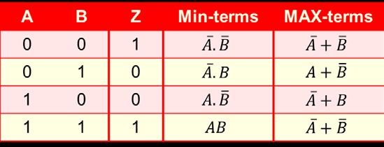
Boolean Algebra
n A truth table specifies output signal logic
values for every possible combination of input
signal logic values
n In evaluating Boolean expressions, the
Operation Hierarchy is: 1) NOT 2) AND 3)
OR. Order can be superseded using ( … )
n Example: A = T , B = F , C = T , D = T
n What is the value of Z = ( A + B ) ⋅ (C + B ⋅ D ) ?
Z = (T + F ) ⋅ (C + B ⋅ D) = ( F + F ) ⋅ (C + B ⋅ D)
= F ⋅ (C + B ⋅ D) = F
5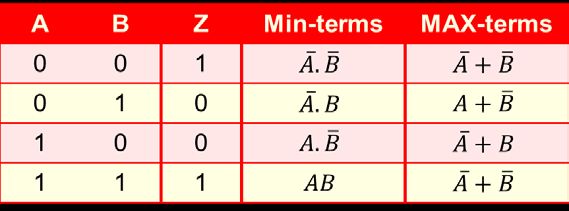
Deriving Logic Expressions From Truth Tables
Light must be ON when both Truth Table:
switches A and B are OFF, or
when both of them are ON. A B Z
0 0 1
0 1 0
SW.A 1 0 0
Logic Function Z (light) 1 1 1
SW.B
n What is the Boolean expression for Z?
6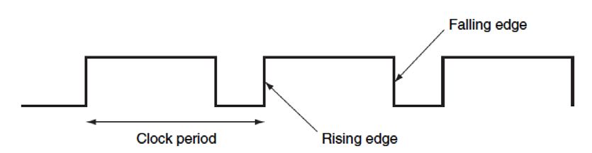
Minterms and Maxterms
n Minterms
n AND term of all input variables.
n For variables with value 0, apply complements
n Maxterms
n OR factor with all input variables
n For variables with value 1, apply complements
A B Z Minterms Maxterms
0 0 1 A+ B
0 1 0
1 0 0
1 1 1
7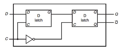
Minterms and Maxterms
n A function with n variables has 2n minterms (and
Maxterms) – exactly equal to the number of rows in
truth table
n Each minterm is true for exactly one combination of
inputs
n Each Maxterm is false for exactly one combination of
inputs
A B Z Minterms Maxterms
0 0 1 A+ B
0 1 0
1 0 0
1 1 1
8Equivalent Logic Expressions
n Two equivalent logic expressions can
be derived from Truth Tables:
1. Sum-of-Products (SOP) expressions:
n Several AND terms OR’d together, e.g.
ABC + ABC + ABC
2. Product-of-Sum (POS) expressions:
n Several OR terms AND’d together, e.g.
( A + B + C )( A + B + C )
9Rules for Deriving SOP Expressions
1. Find each row in TT for which output is 1 (rows
1 & 4)
2. For those rows write a minterm of all input
variables.
3. OR together all minterms found in (2):
Such an expression is called a Canonical SOP
A B Z Minterms Maxterms
0 0 1 A+ B Z = A B + AB
0 1 0
1 0 0
1 1 1
10Rules for Deriving POS Expressions
1. Find each row in TT for which output is 0
(rows 2 & 3)
2. For those rows write a maxterm
3. AND together all maxterm found in (2):
Such an expression is called a Canonical
POS.
A B Z Minterms Maxterms
0 0 1 A+ B
0 1 0
Z = ( A + B )( A + B )
1 0 0
1 1 1
11CSOP and CPOS
n Canonical SOP: Z = A B + AB
n Canonical POS: Z = ( A + B )( A + B )
n Since they represent the same truth
table, they should be identical
Verify that
Z = A B + AB ≡ ( A + B )( A + B )
n CPOS and CSOP expressions for the
same TT are logically equivalent. Both
represent the same information.
12Activity 1
Derive SOP and POS expressions for the
following TT.
A B Carry
0 0 0
0 1 0
1 0 0
1 1 1
13Boolean Identities
Boolean Identities
n Useful for simplifying logic equations.
1
2
3
4
5
6
7
8
9
10
11
12
13
Duals
15Boolean Identities
Identities Property
Single variable, foundations of Boolean
1-5
manipulation
6 Commutative
7 Associative
8 Distributive
9 De Morgan’s
10 Combining
11 Absorption
13 Consensus
16Boolean Identities
n The right side is the dual of the left side
1. Duals formed by replacing
AND OR
OR AND
0 1
1 0
2. The dual of any true statement in Boolean
algebra is also a true statement.
17Boolean Identities
^ DeMorgan’s laws very useful: 9a and 9b
A + B = A.B
NOR gate Alt gate rep.
AB = A + B
Alt gate rep.
NAND gate
18Activity 2
Proofs of some Identities:
12b: A + AB = A + B
13a: AB + AC + BC = AB + AC
19Simplifying Logic Expressions Using Boolean Identities
Simplifying Logic Equations – Why?

A
B             (a) Canonical sum-of-products
                         F = A.B + A.B + A.B
                        F

                            F = A+ B
                  A
                                         F
                  B

                (b) Minimal-cost realization
                                             21
Simplifying Logic Equations
n Simplifying logic expressions can lead to using smaller
number of gates (parts) to implement the logic expression
n Can be done using
n Boolean Identities (algebraic)
n Karnaugh Maps (graphical)
n A minimum SOP (MSOP) expression is one that has no
more AND terms or variables than any other equivalent
SOP expression.
n A minimum POS (MPOS) expression is one that has no
more OR factors or variables than any other equivalent
POS expression.
n There may be several MSOPs of an expression
22Example of Using Boolean Identities
n Find an MSOP for
F = XW + Y + Z (Y + XW )
= XW + Y + ZY + Z XW
= XW (1 + Z ) + Y (1 + Z )
= XW + Y
23Activity 3
n Find an MSOP for
F = VW XY +VWYZ +V XYZ
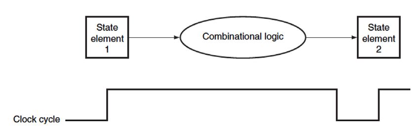
24CSE 2021 Computer Organization Combinational and Sequential Circuits
Digital Circuit Classification
n Combinational circuits
n Output depends only solely on the current
combination of circuit inputs
n Same set of input will always produce the same
outputs
n Consists of AND, OR, NOR, NAND, and NOT gates
n Sequential circuits
n Output depends on the current inputs and state of the
circuit (or past sequence of inputs)
n Memory elements such as flip-flops and registers are
required to store the “state”
n Same set of input can produce completely different
outputs
26CSE 2021 Computer Organization Combinational Circuits
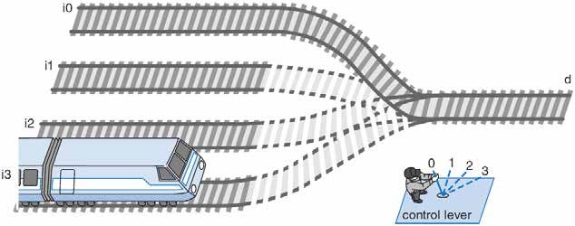
Multiplexer
n A multiplexer (MUX) selects data from one of
N inputs and directs it to a single output, just
like a railyard switch
n 4-input Mux needs 2 select lines to indicate which
input to route through
n N-input Mux needs log2(N) selection lines
28Multiplexer (2)
n An example of 4-input Mux
4-input MUX Actual truth table would
I0 have 26 rows
I0
corresponding to I0, I1,
I1 Z I1
I2, I3, S0 and S1
I2 Z
I3
In-1 S1 S0 Z
S1 S0
0 0 I0
Selection 0 1 I1
control Functional block diagram 1 0 I2
1 1 I3
Condensed truth table
29Decoder
n A decoder is a circuit element that will decode an
N-bit code.
n It activates an appropriate output line as a
function of the applied N-bit input code
Truth Table
3-to-8 decoder
A2 A1 A0 Z0 Z1 Z2 Z3 Z4 Z5 Z6 Z7
Z0
0 0 0 1 0 0 0 0 0 0 0
A2 Z1
0 0 1 0 1 0 0 0 0 0 0
Z2
Z3
0 1 0 0 0 1 0 0 0 0 0
A1 0 1 1 0 0 0 1 0 0 0 0
Z4
Z5 1 0 0 0 0 0 0 1 0 0 0
A0 Z6 1 0 1 0 0 0 0 0 1 0 0
Z7 1 1 0 0 0 0 0 0 0 1 0
1 1 1 0 0 0 0 0 0 0 1
Functional block diagram
30CSE 2021 Computer Organization Sequential Circuits
Why Bit Storage ?
3.2
n Flight attendant call button Call Blue light
n Press call: light turns on
button Bit
Cancel Storage
n Stays on after button
button
released 1. Call button pressed – light turns on
n Press cancel: light turns off Call Blue light
button Bit
n Logic gate circuit to implement
a
Cancel Storage
button
this?
Call Q 2. Call button released – light stays on
Cancel
a
Call Blue light
Doesn’t work. Q=1 when Call=1, but button Bit
doesn’t stay 1 when Call returns to 0 Cancel Storage
button
Need some form of “memory” in the circuit
3. Cancel button pressed – light turns off
32Bit Storage Using SR Latch
n Simplest memory elements are Latch and
Flip-Flops
n SR (set-reset) latch is an un-clocked latch
n Output Q=1 when S=1, R=0 (set condition)
n Output Q=0 when S=0, R=1 (reset condition)
n Problem - Q is undefined if S=1 and R=1
Call S
but t on
Blue light
Q
Cancel
but t on
R
33Clocks
n Clock period: time interval between Freq Period
pulses
100 GHz 0.01 ns
n example: period = 20 ns 10 GHz 0.1 ns
1 GHz 1 ns
n Clock frequency: 1/period 100 MHz 10 ns
n example: frequency = 1 / 20 ns = 50 10 MHz 100 ns
MHz
n Edge-triggered clocking: all state
changes occur on a clock edge.
34Clock and Change of State
n Clock controls when the state of a memory
element changes
n Edge-triggered clocking: all state
changes occur on a clock edge.
35Clock Edge Triggered Bit Storage
n Flip-flop - Bit storage that stores on clock edge, not level
n D Flip-flop
n Two latches, master and slave latches.
n Output of the first goes to input of second, slave latch has inverted
clock signal (falling-edge trigger)
36Setup and Hold Time
n Setup time
n The minimum amount of time the data signal should
be held steady before the clock edge arrives.
n Hold time
n The minimum amount of time the data signal should
be held steady after the clock edge.
37N-Bit Register
n Cascade N number of D flip-flops to form a
N-bit register
n An example of 8-bit register formed by 8
edge-triggered D flip-flops
38CSE 2021 Computer Organization Verilog Basics
What is an HDL?
n A Hardware Description Language (HDL) is
a software programming language used to
model the intended operation of a piece of
hardware.
n The difference between an HDL and “C”
n Concurrency
n Timing
n A powerful feature of the Verilog HDL is
that we can use the same language for
describing, testing and debugging the
system. 40An Example
module pound_one;
reg [7:0] a,a$b,b,c; // register declarations
reg clk;
initial
begin
clk=0; // initialize the clock
c = 1;
forever #25 clk = !clk;
end
/* This section of code implements
a pipeline */
always @ (posedge clk)
begin
a = b;
b = c;
end
endmodule
41Identifiers
n Identifiers are names assigned by the user
to Verilog objects such as modules,
variables, tasks etc.
n An identifier may contain any sequence of
letters, digits, a dollar sign '$' , and the
underscore '_' symbol.
n The first character of an identifier must be
a letter or underscore; it cannot be a dollar
sign '$' , for example. We cannot use
characters such as '-' (hyphen), brackets,
or '#' in Verilog names (escaped identifiers
are an exception). 42Escaped Identifiers
n The use of escaped identifiers allow any character
to be used in an identifier.
n Escaped identifiers start with a backslash (\) and end with
white space (White space characters are space, tabs,
carriage returns).
n Gate level netlists generated by EDA tools (like DC) often
have escaped identifiers
n Examples:
n \/clock = 0;
n \a*b = 0;
n \5-6
n \bus_a[0]
n \bus_a[1]
43module identifiers; /* Multiline comments in Verilog look like C comments
and // is OK in here. */
// Single-line comment in Verilog.
reg legal_identifier, two__underscores;
reg _OK,OK_,OK_$,OK_123,CASE_SENSITIVE, case_sensitive;
reg \/clock ,\a*b ; // Add white_space after escaped identifier.
//reg $_BAD,123_BAD; // Bad names even if we declare them!
initial begin
legal_identifier = 0; // Embedded underscores are OK,
two__underscores = 0; // even two underscores in a row.
_OK = 0; // Identifiers can start with underscore
OK_ = 0; // and end with underscore.
OK$ = 0; // $ sign is OK.
OK_123 =0; // Embedded digits are OK.
CASE_SENSITIVE = 0; // Verilog is case-sensitive (unlike VHDL).
case_sensitive = 1;
\/clock = 0; // An escaped identifier with \ breaks rules
\a*b = 0; // but be careful to watch the spaces!
$display("Variable CASE_SENSITIVE= %d",CASE_SENSITIVE);
$display("Variable case_sensitive= %d",case_sensitive);
$display("Variable \/clock = %d",\/clock );
$display("Variable \\a*b = %d",\a*b );
end An Example44
endmoduleSimulation Result of the Example
Variable CASE_SENSITIVE= 0
Variable case_sensitive= 1
Variable /clock = 0
Variable \a*b = 0
45Logic values
n Verilog has 4 logic Values:
n ‘0’ represents zero, low, false, not asserted.
n ‘1’ represents one, high, true, asserted.
n ‘z’ or ‘Z’ represent a high-impedance value,
which is usually treated as an 'x' value.
n ‘x’ or ‘X’ represent an uninitialized or an
unknown logic value--an unknown value is
either '1' , '0' , 'z' , or a value that is in a state of
change.
46Data Types
n Three data type classes:
n Nets
n Physical connections between devices
n Example: wire a, b;
n Registers
n Storage devices, variables.
n Example: reg a; reg [7:0] bus;
n Parameters
n Constants
n Example: parameter width=32;
parameter A_string =“hello”;
47CSE 2021 Computer Organization Code Structure Design Entities Verilog Module Basics
Design Entities
n The module is the basic unit of code in the
Verilog language.
n Example
module holiday_1(sat, sun,weekend);
input sat, sun;
output weekend;
assign weekend = sat | sun;
endmodule
49module name (port_names);
Verilog Module module port declarations
data type declarations
procedural blocks
^ Modules contain continuous assignments
^ declarations user defined tasks & functions
^ functionality
primitive instances
module instances
^ timing specify blocks
endmodule
syntax:
module module_name (signal, signal,... signal ) ;
. ; //content of module
.
..
.
endmodule
50Module Port Declarations
n Scalar (1bit) port declarations:
n port_direction port_name, port_name ... ;
n Vector (Multiple bit) port declarations:
n port_direction [port_size] port_name, port_name ... ;
n port_direction : input, inout (bi-directional) or output
n port_name : legal identifier
n port_size : is a range from [msb:lsb]
input a, into_here, george; // scalar ports
input [7:0] in_bus, data; //vectored ports
output [31:0] out_bus; //vectored port
inout [maxsize-1:0] a_bus; //parameterized port
51Module Instances
^ A module may be instantiated within another module.
^ There may be multiple instances of the same module.
syntax for instantiation:
module_name instance_name (signal, signal,...);
module example (a,b,c,d);
input a,b;
output c,d;
. . . .
endmodule
example ex_inst_1(in_1, in_2, w, z);
example ex_inst_2(in_1, in_2, , z); // skip a port
52Gate-level Primitives
n Verilog has pre-defined primitives that implement
basic logic functions.
n Structural modeling with the primitives is similar
to schematic level design.
and nand or nor xor xnor
buf not bufif0 bufif1 notif0 notif1
module
gate_level_ex(in_1,in_2,c);
output c;
input in_1,in_2;
in_1 a b
nand (a, in_1, in_2); in_2 c
not (b, a);
or or_1(c, in_2, b); or_1
endmodule
53Activity 4
Given the circuit below, develop a Verilog
module for the circuit
set q
n1
qBar
clear n2
54User-Defined Primitives
n We can define primitive gates (a user-defined
primitive or UDP) using a truth-table specification.
The first port of a UDP must be an output port, and
this must be the only output port (we may not use
vector or inout ports).
n An example
primitive Adder(Sum, InA, InB);
output Sum;
input InA, InB;
table // inputs : output
00 : 0;
01 : 1;
10 : 1;
11 : 0;
endtable
endprimitive
55Operators
n Verilog operators (in increasing order of precedence)
n ?: (conditional)
n || (logical or)
n && (logical and)
n | (bitwise or)
n ~| (bitwise nor)
n ^ (bitwise xor)
n ^~ ~^ (bitwise xnor, equivalence)
n & (bitwise and)
n ~& (bitwise nand)
n == (logical) != (logical) === (case) !== (case)
n < (lt)
n (gt)
n >= (gt or equal)
n > (shift right)
n + (addition)
n - (subtraction)
n * (multiply)
n / (divide)
n % (modulus) 56CSE 2021 Computer Organization Procedural Assignment Continuous Assignment Control Statement
Procedures
n A Verilog procedure is an always or
initial statement, a task , or a function .
n The statements within a sequential block
(statements that appear between a begin
and an end ) that is part of a procedure
execute sequentially in the order in which
they appear, but the procedure executes
concurrently with other procedures.
58Procedural Blocks
n There are two types of procedural blocks:
n initial blocks - executes only once
n always blocks - executes in a loop
n Multiple Procedural blocks may be used, if so the
multiple blocks are concurrent.
n Procedural blocks may have:
n Timing controls - which delays when a statement may be
executed
n Procedural assignments
n Programming statements
59Procedural Statement Groups
n When there is more than one statement within a
procedural block the statements must be grouped.
n Sequential grouping: statements are enclosed within
the keywords begin and end.
n An example
always
begin
a = 5; // executed 1st
c = 4; // executed 2nd
wake_up = 1; // executed 3rd
end
60Timing Controls (procedural delays)
n #delay - simple delay
Delays execution for a specific number of time steps.
n
#5 reg_a = reg_b;
n @ (edge signal) - edge-triggered timing control
nDelays execution until a transition on signal occurs.
n edge is optional and can be specified as either posedge or
negedge.
nSeveral signal arguments can be specified using the
keyword or.
nAn example : always @ (posedge clk) reg_a = reg_b;
n wait (expression) - level-sensitive timing control
nDelays execution until expression evaluates true.
nwait (cond_is_true) reg_a = reg_b;
61Procedural assignments
n Assignments made within procedural
blocks are called procedural assignments.
n Value of the RHS of the equal sign is
transferred to the LHS
n LHS must be a register data type (reg,
integer, real). NO NETS!
n RHS may be any valid expression or signal
always @ (posedge clk)
begin
a = 5; // procedural assignment
c = 4*32/6; // procedural assignment
wake_up =$time; // procedural assignment
end
62Continuous Assignment
n Continuous assignment assigns a value to a
wire in a similar way that a real logic gate
drives a real wire.
n The main use for continuous assignments is to
model combinatorial logic.
syntax: Explicit continuous assignment:
assign net_name = expression;
where net_name is a net that has been previously declared
module continuous (Ain, Aout);
input Ain;
output Aout;
assign Aout = ~Ain //continuous assignment.
endmodule Aout
Ain
63Illustration of Assignment Statements
module assignments
//... Continuous assignments go here.
always // beginning of a procedure
begin // beginning of sequential block
//... Procedural assignments go here.
end
endmodule
64Control Statements
n Two types of programming statements:
n Conditional
n Looping
n Programming statements only used in
procedural blocks
65if and if-else
syntax:
if(expression) statement
If the expression evaluates to true then execute the statement
if(expression) statement1
else statement2
If the expression evaluates to true then execute statement1,
if false, then execute statement2.
module if_ex(clk);
input clk;
reg red,blue,pink,yellow,orange,color,green;
always @ (posedge clk)
if (red || (blue && pink))
begin
$display ("color is mixed up");
colorfor
syntax:
for (assignment_init; expression; assignment)
statement or statement_group
^ The assignment_init is executed once at the start of
the loop.
^ Loop executes as long as expression is true.
^ The assignment is executed at the completion of
each loop.
module for_ex1 (clk);
input clk;
reg [31:0] mem [0:9]; // 10x32 memory
integer i;
always @ (posedge clk)
for (i = 9; i >= 0; i = i-1)
mem[i] = 0; // init the memory to zeros
endmodule
67Simulating the Verilog Code
nVerilog code of NAND Latch
Module simple_latch (q, qBar, set, clear);
input set, clear;
output q, qBar;
nand #2 n1(q,qBar,set);
nand #2 n2(qBar,q,clear);
endmodule set q
n1
qBar
clear n2
68Testbench
n A testbench generates a sequence of input
values (we call these input vectors ) that
test or exercise the verilog code.
n It provides stimulus to the statement that
will monitor the changes in their outputs.
n Testbenchs do not have a port declaration
but must have an instantiation of the circuit
to be tested.
69A testbench for NAND Latch
Module test_simple_latch;
wire q, qBar;
reg set, clear;
simple_latch SL1(q,qBar,set,clear);
initial
begin
#10 set = 0; clear = 1;
#10 set = 1;
#10 clear = 0;
#10 clear = 1;
#10 $stop;
#10 $finish;
end
initial
begin
$monitor (“%d set= %b clear= %b q=%b qBar=%b”,$time,
set,clear,q,qBar);
end
endmodule
70You can also read