Design and Optimization Power in 10T SD RAM with Voltage Etimation using Artficial Intelligence - ijsret
←
→
Page content transcription
If your browser does not render page correctly, please read the page content below
International Journal of Scientific Research & Engineering Trends
                                                Volume 7, Issue 3, May-June-2021, ISSN (Online): 2395-566X

   Design and Optimization Power in 10T SD RAM with
       Voltage Etimation using Artficial Intelligence
                                              Priya Jain, Mrs. Megha Soni
                                          Department of Electronics & Communication,
                                           Swami Vivekanand College of Engineering,
                                                       Indore,M.P.,India

Abstract- Random access memory is an essential resource required by the computational hardware. As the processor speed has
attained GHz clock frequency, memory throughput can be a bottleneck to achieve high performance. 10T SDRAM can deliver
a reasonable solution for such data storage. Typical computational system consists of multiple hardware modules that perform
different operations on the data. These modules attempt to access the data concurrently. This leads to a requisite for a memory
controller that arbitrates amid requests queried by different modules and exploits maximum throughput. The memory
controller interfaces SDRAM and other subsystems. Hence it manages the data into and out of memory. The access latency or
access speed solely depends on the implementation of memory controller. We are also proposed on AI algorithm because it is
consume lower power as compare to AI. The study comprises area, power and timing analysis of the both in AI based 10T
SDRAM. Synopsys Design Compiler tool is used to obtain the necessary results. Conventional 10T SDRAM and MESFET 10T
SDRAM are analyzed through Microwind and DHCH tool in technology. It is seen that sub-threshold and gate leakage, both
effects the operation of the SSDRAM cell. In this thesis MESFET is used to simulate the 10T SDRAM cell and it is concluded
that MESFET increases the performance of SDRAM cell.

Keywords- SDRAM, DDR, Microwind, MATLAB, ANN, AI.

                                                                 SDRAM stores each bit of data in a separate passive
                I. INTRODUCTION                                  electronic component that is inside an integrated circuit
                                                                 board. Each electrical component has two states of value
The motivation behind designing the processor is to              in one bit called 0 and 1.
increase its speed so that our task becomes too fast. In this
research we tried to find some of the techniques to reduce       This captivator needs to be refreshed often otherwise
the processing time of the processor. A processor is             information fades. SDRAM has one capacitor and one
something which processes the given task. It is developed        transistor per bit as opposed to static random access
to make human task easy, and when it processes micro             memory (SSDRAM) that requires 6 transistors. The
things it is called as a microprocessor. It contains basically   capacitors and transistors that are used are exceptionally
two things. One is the CPU and second is the memory.             small. There are millions of capacitors and transistors that
CPU stands for central processing unit [1].                      fit on one single memory chip.

It controls the whole processor; we can also call it a           With the rapid development in the processor’s family,
human brain. The design of processor needs the designing         speed and capacity of a memory device is a major concern.
of CPU and memory. The memory can be static or                   The DDR is an enhancement to the traditional
random. Design of CPU can be done in different ways but          synchronous SDRAM. The DDR is able to transfer the
its fundamental operation remains the same.                      data on both the edges of each clock cycle. Thus doubling
                                                                 the data transfer rate of the memory device.
CPU is designed on small scale and large scale integration.
Processors are designed with enhancements like                   The DDR is available in a very low cost that’s why it is
decreasing power consumption, increasing more pipeline           widely used in personal computers where they are
stages, increasing speed and minimizing the chip area. The       basically used to provide the functions of storage and
basic operation performed by a processor is fetching,            buffers. The DDR SDRAM supports the data widths of 16,
decoding and executing the given instruction. After that         32 and 64 bits. It automatic refresh during the normal and
the output will store in memory. For storing the results in      power down modes. The DDR is a complete synchronous
memory some mechanism is applied. Dynamic random                 implementation of controller. It increases the throughput
access memory (SDRAM) is a type of random-access                 using command pipelining and bank management. This
memory used in computing devices (primarily PCs).                improvement allows the DDR module to transfer data
                                                                 twice as fast as SDRAM. As an example, instead of a data
                                                       © 2021 IJSRET
                                                            1265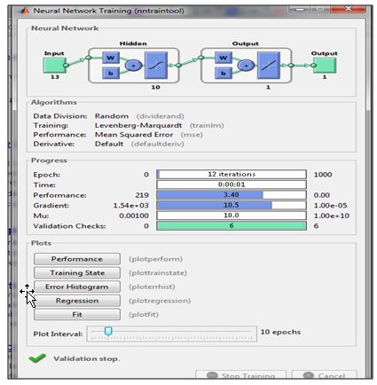
International Journal of Scientific Research & Engineering Trends
                                              Volume 7, Issue 3, May-June-2021, ISSN (Online): 2395-566X

rate of 133MHz, DDR memory transfers data at 266MHz.          nonvolatile memory and can last longer even after the
DDR modules, like their SDRAM predecessors, arrive in         power is off.
there.
                                                              The classification of memory is as follows-
Although motherboards designed to implement DDR are           1.1 Random Access Memory: Random access memory
similar to those that use SDRAM on motherboards that are      (RAM) is the best known form of computer memory.
designed for DDR. SDRAM, they are not backward                RAM is considered "random access" because you can
compatible with motherboards that support SDRAM. You          access any memory cell directly if you know the row and
cannot use DDR in earlier SDRAM based motherboards,           column that intersect at that cell. RAM data, on the other
nor can you use SDRAM on motherboards that are                hand, can be accessed in any order. All the data that the
designed for DDR.                                             PC uses and works with during operation are stored here.
                                                              Data are stored on drives, typically the hard drives.
  II. PROCESSOR ARCHITECTURE AND                              However, for the CPU to work with those data, they must
          ITS FUNDAMENTALS                                    be read into the working memory storage (RAM).

A processor takes input information, processes that input     Types of Random Access Memory:
and produces output result which gets stored inside the       1.1.1 Static Random Access Memory: Static Random
memory [2]. This is the fundamental operation of a            Access Memory uses a completely different technology. In
processor. The functional units of a processor are input      static RAM, a form of flip-flop holds each bit of memory.
output, memory storage, arithmetic logic unit and control     A flip-flop for a memory cell takes four or six transistors
unit. Information in a processor is in the form of data. In   along with some wiring, but never has to be refreshed.
terms of technical language we can define this data in bits   This makes static RAM significantly faster than dynamic
or bytes. The memory of the processor can be increased as     RAM.
per need.
                                                              However, because it has more parts, a static memory cell
Information in a processor is known as instruction which      takes up a lot more space on a chip than a dynamic
is given by an human operator. There is a particular          memory cell. Therefore, you get less memory per chip.
language for the understanding of processor called as         Static Random Access Memory uses multiple transistors,
assembly language. It contains the instruction sets. A        typically four to six, for each memory cell but doesn't have
sequence of instruction is called as program. Processor       a capacitor in each cell. It is used primarily for cache. So
fetches instructions that make up a program from the          static RAM is fast and expensive, and dynamic RAM is
memory and performs the operations stated in those            less expensive and slower. So, static RAM is used tocreate
instructions. There are n no of programs written for a        the CPU's speed-sensitive cache, while dynamic RAM
process.                                                      forms the larger system RAM space.
 \
                                                              1.1.2 Dynamic Random Access Memory:
                                                              Dynamic Random Access Memory has memory cells with
                                                              a paired transistor and capacitor requiring constant
                                                              refreshing. SDRAM works by sending a charge through
                                                              the appropriate column (CAS) to activate the transistor at
                                                              each bit in the column. When writing the row lines contain
                                                              the state the capacitor should take on. When reading the
                                                              sense amplifier determines the level of charge in the
                                                              capacitor. If it is more than 50 percent, it reads it as a 1
                                                              otherwise it reads it as a 0.

                                                              A memory chip rating of 70ns means that it takes 70
                                                              nanoseconds to completely read and recharge each cell. It
                                                              is one of the most common types of computer memory
 Fig 1. Overview of the SDRAM based RISC processor.           (RAM). It can only hold data for a short period of time and
                                                              must be refreshed periodically. SDRAMs are measured by
1. Memory:                                                    storage capability and access time. Storage is rated in
Memory unit stores instructions and data. There are           megabytes (8 MB, 16 MB, etc). Access time is rated in
mainly two types of memory. The first is volatile and         nanoseconds (60ns, 70ns, 80ns, etc) and represents the
second is nonvolatile. Random Access Memory (RAM), is         amount of time to save or return information. With a 60ns
a volatile memory that stores information on an integrated    SDRAM, it would require 60 billionths of a second to save
circuit, whereas ROM (Read only memory) is a                  or return information. The lower the speed, the faster the
                                                              memory operates. SDRAM chips require two CPU wait

                                                     © 2021 IJSRET
                                                         1266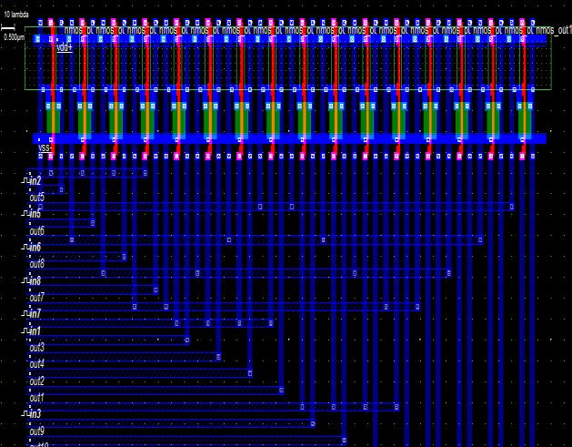
International Journal of Scientific Research & Engineering Trends
Volume 7, Issue 3, May-June-2021, ISSN (Online): 2395-566X
states for each execution. Canonly execute either a read or and sold in a variety of packages, their overall operation is
write operation at one time. The capacitor in a dynamic essentially the same. SDRAMs are designed for the sole
RAM memory cell is like a leaky bucket. It needs to be purpose of storing data. The only valid operations on a
refreshed periodically or it will discharge to 0. This refresh memory device are reading the data stored in the device,
operation is where dynamic RAM gets its name. Memory writing (or storing) data in the device, and refreshing the
is made up of bits arranged in a two-dimensional grid. In data periodically. To improve efficiency and speed, a
which memory cells are fetched onto a silicon wafer in an number of methods for reading and writing the memory
array of columns (bit lines) and rows (word lines). have been developed.
The intersection of a bit line and word line constitutes the Synchronous SDRAM (Dynamic Random Access
addressof the memory cell. Memory cells alone would be Memory) is the main memory used for all desktop and
worthless without some way to get information in and out larger computers. Each elementary SDRAM cell is made
of them. So the memory cells have a whole support up of a single MOS transistor and a storage capacitor
infrastructure of other specialized circuits. (Figure 3.1).
Identifying each row and column (row address select and Each storage cell contains one bit of information. This
column address select) Keeping track of the refresh charge, however, leaks off the capacitor due to the sub-
sequence (counter) Reading and restoring the signal from threshold current of the cell transistor. Therefore, the
a cell (sense amplifier) Telling a cell whether it should charge must be refreshed several times each second.
take a charge or not (write enable) Other functions of the
memory controller include a series of tasks that include
identifying the type, speed and amount of memory an
checking for errors. The traditional RAM type is SDRAM
(dynamic RAM). The other type is SSDRAM (static
RAM). SSDRAM continues to remember its content,
while SDRAM must be refreshed every few milliseconds.
III. PROBLEM STATEMENT
Multiprocessor SDRAM systems can solve problems
many times faster than a single processor alone. However,
these processors must communicate in order to efficiently
divide and solve a problem. Fast volatile memory is
designed for use with a single processing system. In order
for multiprocessor systems to access a common resource
such as a memory, there must be some facilitation between
the processing systems and the memory, in order to avoid Fig 2. SDRAM Cell.
any data corruption or malfunctioning of the system. [1]
This is where the arbiter comes into play. An arbiter can 1.1 How the device works?
be considered as a controlling system, which can be The memory cell is written to by placing a “1” or “0”
incorporated in between the multiprocessor systems and charge into the capacitor cell. This is done during a write
the shared memory. The arbiter follows a set of rules to cycle by opening the cell transistor (gate to power supply
pass the communication between the various processing or VCC) and presenting either VCC or 0V (ground) at the
systems. capacitor. The word line (gate of the transistor) is then
held at ground to isolate the capacitor charge. This
IV. OBJECTIVES OF RESEARCH WORK capacitor will be accessed for either a new write, a read, or
a refresh.
Following research objectives are as follow some points –
To observation of proposed design based power Figure 3-2 shows a simplified SDRAM diagram. The gates
consumption. of the memory cells are tied to the rows. The read (or
Reduction of leakage current. write) of a SDRAM is done in two main steps as
Improvement of system model performance. illustrated in Figure 3-3. The row (X) and column (Y)
addresses are presented on the same pads and multiplexed.
1. Synchronous Dynamic Random Access Memory The first step consists of validating the row addresses and
(SDRAM): the second step consists of validating the column
Synchronous Dynamic Random Access Memory addresses.
(SDRAM) devices are used in a wide range of electronics
applications. Although they are produced in many sizes
© 2021 IJSRET
1267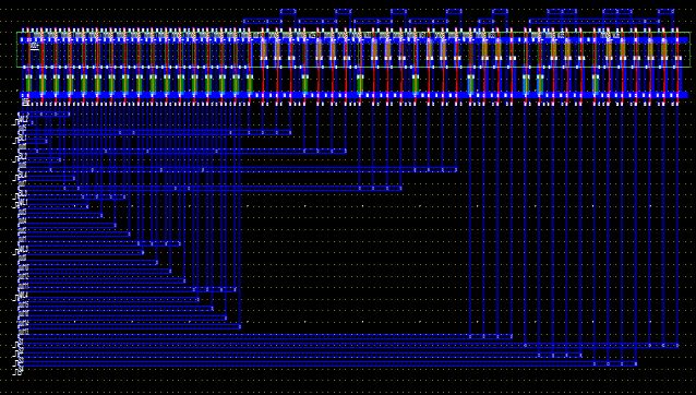
International Journal of Scientific Research & Engineering Trends
                                              Volume 7, Issue 3, May-June-2021, ISSN (Online): 2395-566X

                                                              requires named preparing information, while the last just
                                                              uses unlabeled preparing information. In regulated
                                                              learning, the goal for an operator is to take in a
                                                              parameterized work from the given marked preparing
                                                              dataset and afterward dependent on the capacity learntto
                                                              anticipate the outcome straight forwardly while new
                                                              information shows up.

                                                              The regular errands in directed learning are relapse and
                                                              classification. Specifically, relapse is to decide the
                                                              quantitative connection between specific factors dependent
                                                              on a lot of preparing information, and classification is to
                                                              find a capacity to decide the class to which the information
                                                              has a place.
             Fig 3. SDRAM Access Timing.
                                                              3. Introduction - Artificial Neural Networks (ANN):
1.2 Memory cell:                                              ANN is the term used for systems that attempt to work the
A great deal of design effort has been made to shrink the     approach the human brain works. Suggests that system
cell area, particularly, the size of the SDRAM capacitor.     tries to perform a precise task the approach humans do.
As memory density increases, the cell size must decrease.     commonly computers do any work the approach it's
Designers have managed to shrink overall cell size.           educated within the sort of code, however it doesn't have
However, due to factors such as noise sensitivity and         the aptitude of finishing works that it absolutely was ne'er
speed, it has been a challenge to reduce the capacitance.     schooled of however if we tend to contemplate an
                                                              individual's brain, it's self-learning capability that makes it
The capacitance must stay in the range of 30fF. The           perform several processes that it's been neither performed
charge (Q) stored in a capacitor is equal to capacitance      nor schooled.
times voltage (Q = C x V). Over the years, SDRAM
operating voltage has decreased (i.e., 12V to 5V to 3.3V).    So, ANN essentially tries to inherit this capability of the
As voltage decreases, the stored charge will also decrease.   human brain to self-train itself for tasks that area unit ne'er
Design improvements allow for the decrease in the cell        been performed by it that too terribly with efficiency.
charge as long as the capacitance remains in the range of     Human brain’s structure consists of neurons that area unit
30fF.                                                         interconnected with one another and there by forming
                                                              giant network that is well connected thereby helps in
Two main developments are used to reduce capacitor area       playing a awfully complicated task like voice and image
without reducing its value. These are the use of new          recognition very simply. A similar task once performed
capacitor shapes to fit into a minimum chip surface area      mistreatment traditional pc will not offer an correct result.
and increasing the dielectric constant.
                                                              Hence ANN mimics neurons structure of the human brain
2. Overview of Machine Learning Techniques:                   to get the link between input and targets. Neurons have
As the center strategy of AI, AI (ML) is a multi-             this ability to avoid wasting previous experimental
disciplinary subject including numerous controls, for         information. The speed of human brain is many thousand-
example, likelihood hypothesis, insights, data hypothesis,    time quicker than ancient standard conventional pc as a
computational hypothesis, advancement hypothesis, and         result of in brain in contrast to traditional pc as whole data
software engineering.                                         isn't passed from vegetative cell to vegetative cell they're
                                                              rather encoded within the neuron network. This can be the
T. Mitchell gave a short definition of AI in 1997 as           explanation why the neural network is additionally named
follows: "machine learningis the investigation of PC          as connectionism.
calculations that improve naturally through experience"
[6]. Subsequently, the primary target of ML is to cause
operators to recreate or execute human learning practices.
For instance, with the assistance of ML calculations, a
machine specialist can gain from preparing information to
accomplish various undertakings, for example, picture
acknowledgment.

In view of the sort of preparing information utilized, ML
can be partitioned into two branches, to be specific,
administered learning and unaided learning. The previous                                   (a)
                                                     © 2021 IJSRET
                                                          1268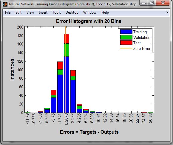
International Journal of Scientific Research & Engineering Trends
Volume 7, Issue 3, May-June-2021, ISSN (Online): 2395-566X
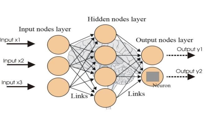
wherever the neuron processes it and generates the
specified output. It ought to be noted although that the
output of a vegetative cell may be fed to a different
vegetative cell. a group of such neurons is termed a neural
network. The transformation of the biological model of
vegetative cell into a mathematical model is shown in
figure 4.2.
V. SIMULATION AND RESULTS
1. Four transistor Dynamic RAM cell:
(b)
Fig 4. Concept of ANN.
A biological model of a vegetative cell is largely
comprised of dendrites, a cell body or soma, And an nerve
fiber as shown in Figure 4.1. The cell body, additionally
known as the soma, holds the nucleus of neurons.
The dendrites square measure the branches that square
measure connected to the cell body and stretched in house
round the cell body to receive signals from neighbour
neurons. The nerve fiber works as a transmitter of the
vegetative cell. It sends signals to neighbour neurons.
The junction or conjunction terminal is that the association
between the nerve fiber of 1 vegetative cell and therefore
the dendrites of neighbour nucleon, that is that the
communication link in between the 2 neurons. chemistry
signals square measure communicated from the junction. Fig 6. Four Transistor Dynamic RAM cell.
once the entire signal received by a vegetative cell is over
the junction threshold, it causes the vegetative cell to
fireplace i.e., send Associate in Nursing chemistry signal
to neighbour neurons. it's assumed that the alteration
exhausted the strength of the conjunction association is
that the main foundation of our brain’s memory [11].
Fig 7. Layout Design Micro-wind.
Table 1. Voltage and Frequency Table.
Voltage Frequency
Fig 5. Mathematical equivalent of Neuron.
50 0.056
This modification is finished in ANN within the type of
100 0.016
weights between neurons so as to perform any kind of
action in our body, completely different components of the 150 0.007
body (sense organs) send signals that travel through
200 0.006
different components and reach the brain vegetative cell’s
© 2021 IJSRET
1269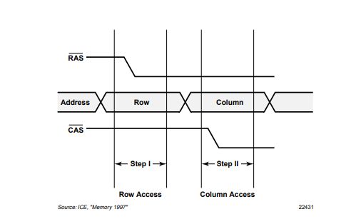
International Journal of Scientific Research & Engineering Trends
                                               Volume 7, Issue 3, May-June-2021, ISSN (Online): 2395-566X

         Fig 8. Voltage and Frequency variation.

    Table 2. Input voltage and power of consumption.                 Fig 10. 10T SDRAM cell Micro-Wind Design.
        Input voltage       Power of consumption
               3                  1.4616µw                         Table 4. Input voltage and power of Consumption.
               4                  1.4617µw                              Input voltage            Power of
                                                                                                Consumption
               5                  1.4626µw
                                                                              3                   0.664µw
               6                  1.4627µw
                                                                              4                   0.665µw
                                                                              5                  0.6666µw
Note: - If (c/ tox(load)=0.029x10⁻¹², f=0.056x10⁶, variable
voltage.)                                                                     6                   0.668µw

 Table 3. Current of Leakage and power of consumption.           Table 5. Current of Leakage and power of consumption.
         Input voltage           Current of                              Input voltage           Current of
                               Leakage(20ns)                                                   Leakage(20ns)
               3                  0.09454mA                                    3                  0.07mA
                                                                               4                  0.07 mA
               4                  0.09455mA
                                                                               5                  0.07mA
               5                  0.09457mA                                    6                  0.07mA
               6                  0.09459mA
                                                              3. MATLAB AI optimization:
2. Proposed AI Design:

         Fig 9. 10T SDRAM cell DSCH Design.                                    Fig 11. NN Training State.

                                                     © 2021 IJSRET
                                                          1270
International Journal of Scientific Research & Engineering Trends
Volume 7, Issue 3, May-June-2021, ISSN (Online): 2395-566X
SDRAM and MESFET 10T SDRAM are analyzed through
cadence virtuoso tool in 45 nm technology. It is seen that
sub-threshold and gate leakage, both effects the operation
of the SSDRAM cell.
In this thesis MESFET is used to simulate the 10T
SDRAM cell and it is concluded that MESFET increases
the performance of SDRAM cell. The considerable change
in the sub-threshold leakage is observed in comparison
with the gate leakage. Total leakage in the SDRAM cell
can be reduced to 10 % using MESFET.
Further technique is applied in MESFET SSDRAM cell in
which LSVL provides increased ground voltage and
USVL provides reduced supply voltage during standby
mode which reduces the leakage by 34 %. Therefore,
results in reduced power dissipation and increased
performance.
Fig 12. Error of histogram.
VII. FUTURE WORK
MSE Analysis represent histogram for multiple layer
option. The irregular result provide to neural network. So Future work would be verification of these memory
0.2678 Error histogram with 20 bins is the highest value of controllers using System Verilog. System Verilog is an
this graph represent. industry standard verification language as it ensures 100%
functional and code coverage in any design. Other value
addition would be application of low power design
techniques in the memory controller design. Low power
methods greatly reduce the overall power intake of the
system.
REFERENCES
[1] J. L. Hennessy, D. A. Patterson, ‘‘Computer
Organization and Design: The Hardware/Software
Interface’’, Second Edition, Morgan Kaufmann, 2003.
[2] M. Shand, “Flexible Image Acquisition using
reconfigurable hardware” In Proc. of the IEEE
Workshop on Field Programmable Custom
Computing Machines, April 1995.
[3] Jen-Shiun Chiang and Jun-Yao Liao, “A novel
asynchronous control unit and the application to a
pipelined multiplier”, IEEE, pp. II 169-172, 1998.
[4] Design and implementation of 5 stage pipelined 32 bit
RISC processor Sharda P. Katke1, G. P. Jain2 ISSN
2250-2459, Volume 2, Issue 4, April 2012.
[5] R. Uma, Pondicherry University, Pondicherry
(IJERA), “Design and performance analysis of 8 bit
Fig 13. Output Error. RISC processor using Xilinx tool”, Vol. 2, Issue 2,
pp.053-058 Mar-Apr 2012.
VI. CONCLUSION [6] Anand Nanda kumar Shardul, “16-Bit RISC Processor
Design for Convolution Application”, International
The feature of good performance, low power consumption Journal of Advancements in Research & Technology,
and low cost. Memory will remain an inevitable Volume 2, Issue 9, ISSN 2278-7763, September-
component and a crucial device in the computational 2013.
arena. With this motive, an implementation of the [7] Seung Pyo Jung, Jingzhe Xu, Donghoon Lee, “Design
SDRAM and SDRAM controller is presented in this paper. & Verification of 16 Bit RISC Processor.
Power and area are two prime gauges in the evaluation of [8] Dimitris Mandalidis1 , Panagiotis Kenterlis2 , John N.
the performance of any digital system. Conventional 10T Ellinas3, “A Computer Architecture Educational
© 2021 IJSRET
1271International Journal of Scientific Research & Engineering Trends
Volume 7, Issue 3, May-June-2021, ISSN (Online): 2395-566X
System based on a 32-bit RISC Processor”,
International Review on Computers and Software
(I.RE.CO.S.), Vol. xx, n. x, 2008.
[9] T. S. Hall and J. O. Hamblen, “System-on-a-
programmable chip development platforms in the
classroom,” IEEE Trans. Educ., vol. 47, no. 4, pp.
502–507, Nov. 2004.
[10] R.Uma,” Design and Performance Analysis of 8-bit
RISC Processor using Xilinx tool”, International
Journal of Engineering Research and Applications
(IJERA), ISSN: 2248-9622, Vol. 2, Issue 2, pp.053-
058 Mar-Apr 2012.
© 2021 IJSRET
1272You can also read