Design of 13.56 MHz Smartcard Stickers with Ferrite for Payment and Authentication
←
→
Page content transcription
If your browser does not render page correctly, please read the page content below
Design of 13.56 MHz Smartcard Stickers with
            Ferrite for Payment and Authentication
         Michael Gebhart, Roland Neubauer, Michael Stark                                 Dimitri Warnez
             NXP Semiconductors Austria GmbH Styria                NXP Semiconductors Germany GmbH
                        Gratkorn, Austria                                 Hamburg, Germany
        gebhart@ieee.org, {roland.neubauer, michael.stark}@nxp.com      dimitri.warnez@nxp.com

   Abstract—We present an adhesive sticker which allows
contactless Smartcard function widely independent of the object                         II. PRINCIPLE OF OPERATION
material which it is sticked to. Recently interest raised for such a
                                                                          Contactless transponder products in the 13.56 MHz range
sticker to be attached on any mobile phone for contactless
payment applications. This is seen as precessor of near field          are powered by the H-field emission of a proximity reader.
communication (NFC) technology helping to introduce                    The magnetic flux of the alternating reader field passes
contactless payment with mobile phone. In this context we              through the turns of the resonant transponder loop antenna in
consider antenna design with field simulation software and             free air and induces voltage. This is required for the Smartcard
evaluate electrical antenna parameters of samples fabricated in        chip operation. In case the transponder is attached closely to a
the Smartcard process flow. Aspects for conformance to the
                                                                       conductive metal case, the reader H-field generates eddy
ISO/IEC14443-2 and NFC card standard are considered and an
optimized composite design is proposed.                                currents in this material, which cause a secondary H-field in
                                                                       phase opposition to the primary field. As a result, depending
                       I. INTRODUCTION                                 on the conductivity of the material, the magnetic flux through
                                                                       the loop antenna is nearly cancelled out. So the transponder is
   Over the last years the mobile phone has developed to a             not powered, therefore the Smartcard function is prohibited.
wireless personal multi-media information center, covering an             To overcome this problem, ferrite material can be inserted
increasing number of applications and being part of the                between antenna loops and metal case. This material will
standard equipment of practically every single person.                 conduct at least a part of the magnetic flux behind the
Additionally, contactless Credit Cards are approaching mass            transponder loop antenna. As a result, eddy currents
market to supplement secure, microcontroller based
                                                                       originating from this part of the magnetic flux are prevented.
applications. The combination of electronic payment and the
                                                                       This kind of magnetic isolation will allow the transponder to
mobile phone is a step further to end up in an all-in-one
                                                                       be powered at least by the part of the magnetic reader flux,
solution. The small form factor of some phones not only
requires a reduction of size, compared to the Credit Card, but         which is conducted by the ferrite sheet.
also different materials used for the phone case, plastic or              The high relative permeability of the ferrite material close
metal, will severely degrade performance of conventional               to the loop antenna will also affect electrical parameters of the
contactless technology. So this requires new antenna design            equivalent antenna circuit and thus must be taken into account
concepts. As a first step, adhesive stickers with ferrite foil         for proper design. The ferrite material will increase the
were developed to be attached on the back side of phones and           antenna inductance. Moreover, there are additional losses in
operate autonomously, before they will be replaced by Near             the ferrite material to be considered. This has drawbacks on
Field Communication (NFC) chips, directly integrated on the            resonance frequency and quality factor of the transponder.
mobile phone printboard and having access to embedded                     In case there is conductive material present behind the
Secure Elements (SE), Secure Device (SD) cards and                     sticker of such a design, the inductance is decreased. So there
Subscriber Identity Modules (SIM) in the phone. A similar              remains still an important dependency of this type of sticker.
example is a contactless module integrated in µSD cards, as            One option to reduce this dependency is to apply a metal layer
proposed by companies like Tyfone [15], G&D [14] and                   (absorber) behind the ferrite. Such a composite design helps in
Device Fidelity. However, further applications for such                two ways: first, the dependency on the phone case material is
stickers are already coming up, e.g. secure authentication of          reduced a lot, so the Smartcard sticker is really “isolated”, and
sealed objects, which in principle have the same requirements          second, it also is shielded from unwanted emissions of a phone
as payment stickers to the contactless technology.                     in plastic case, which at intermediate frequency (IF) level may
   In this paper, we describe the design of 13.56 MHz loop
                                                                       be close to 13.56 MHz and could possibly have an impact on
antennas on ferrite material, to build up composite RFID
                                                                       contactless Smartcard performance.
Smartcard stickers operating nearly independent of any object
material, which they are attached to.
III. SMARTCARD ANTENNAS pressure (e.g. 3.5 kN) over some time (e.g. 3 minutes) to bake
the individual layers to one sheet body, of which the cards are
A. Antenna design framework punched out. Since the antenna wire is embedded in soft
Antennas for contactless near field systems in the 13.56 substrate material (e.g. polyvinyl chloride, PVC), the specified
MHz frequency band are resonant loop antennas. The geometry may be changed in this process (e.g. shrink). The
alternating (active and reactive) current in the antenna production of a series of coils with varied geometry is usually
conductor is related to the alternating H-field in space as denoted as antenna design matrix. The antenna design matrix
described by Maxwells equations [1, 4]. can be further used to fit an analytical model to the process.
Among the general conditions to start antenna design for In this study, we have used the analytical formula approach
cards, stickers or labels are typically: to estimate a series of antenna designs for ferrite stickers of a
• Requirements for the outline of the final product, defined, limited size. A number of samples for each design has
referring to a maximum size for the antenna. been produced with and without chip module assembled, to
• The choice of one out of the four main antenna allow us characterization measurements. In a third step after
production technologies in this context, which are wire measurement, the CAD field simulation software High
embedding, etching, electroplating in a galvanic Frequency Structure Simulator (HFSS) was used to simulate a
process, or printing (e.g. silver ink or paste). design, to see how useful such a tool is in this context (in
• The choice of chip package (e.g. module, or flip-chip). terms of the way how to model the structure, how accurately
• The choice of materials. the results fit to measurements, and how much time and effort
• The choice of an appropriate assembly process, e.g. the calculation takes).
crimping, welding, soldering or conductive glueing, B. Antenna parameter measurement
and last but not least,
Since the planar spiral loop antenna is a distributed element,
• an idea how the application should work, including like for all antennas, the complex impedance varies over
ambient conditions (e.g. temperature, close coupling to frequency. For practical calculations, the electrical properties
metal or other objects) and standard requirements, to be are represented in an equivalent circuit consisting of lumped
interoperable with existing infrastructure. We consider elements. A simple parallel resonant circuit is sufficient to
these aspects in chapter IV. allow considerations for main aspects of high frequency HF
For the actual antenna design there are two approaches: On transponder systems in Smartcard applications, although it is
the one hand analytical formulas, as we have described in important to note this model is only valid precisely for one
previous work [7], allow estimations for simple structures, e.g. frequency.
inductance of a rectangular coil, consisting of a circular wire
conductor, which has little parasitic capacitance. Furthermore,
this approach can easily take into account known process
influences or allows estimations for changes in one parameter. RAS
On the other hand, there is computer aided design software CC RC CAS CA R A LA
(CAD) using the finite element method (FEM). We have used
this approach to re-calculate our measurement results.
RAS
Chip Assembly Antenna
Fig. 2. Equivalent transponder circuit. Lumped elements represent the
Smartcard chip (note that CC and RC are voltage dependent), the assembly
connection of chip and antenna, and the loop antenna (note that CA, RA and LA
are frequency dependent).
The main electrical parameter of the antenna loop coil is the
inductance LA, consisting of some self-inductance due to coil
length and mainly of mutual inductance due to coupling
between the coil turns. In addition, there is also some parasitic
capacitance CA e.g. due to the electric coupling between the
turns, and depending on the relative dielectric constant of the
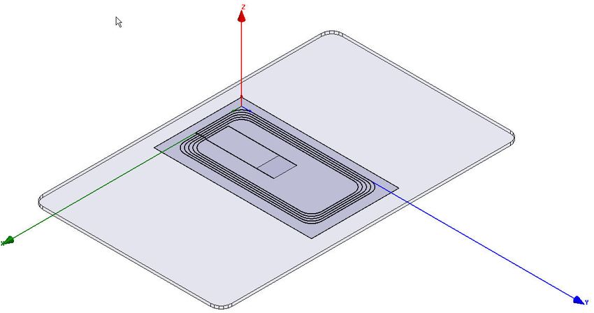
Fig. 1. Geometry for sticker on ferrite foil. 5 antenna designs of the same substrate material. In fact, this causes the reactive part of the
outline have been produced in the typical smartcard production flow. impedance to change over frequency. Starting from inductive
behaviour at low frequencies close to direct current (DC), the
The sticker product can be laminated in a card process,
reactive impedance varies to a frequency where it becomes
which allows to use already existing machines e.g. for
zero and which is defined as the self-resonance frequency fS of
personalization in the further process flow. The lamination
the antenna, to a capacitive behaviour.
process means to apply high temperature (e.g. 140 °C) andFor our considerations, a series of 5 embedded wire antenna
inductive behaviour
designs with equal outline and varied pitch – the spacing
inductance
between antenna turns – was produced on 200 µm PVC
best point to read out self-resonance substrate and laminated with 2 x 50 µm ferrite foils of 45 x 25
coil inductance frequency mm size. The antenna parameters for an equivalent parallel
resonant circuit, measured as described above, are given in
frequency table 1. For comparison the antennas were also measured as
0 air coils on PVC substrate, with the ferrite sheets removed.
TABLE I
instrument STICKER ANTENNA GEOMETRICAL AND ELECTRICAL PARAMETERS
cut-off frequency Antenna geometry data
No 1 No 2 No 3 No 4 No 5
inaccurate outline mm 40 x 20
wire diam. µm 100
range cap. behaviour pitch mm 0.2 0.5 0.6 0.4 0.2
turns 4 4 5 5 5
Fig. 3. Typical measurement trace of coil inductance over frequency. Equivalent circuit electrical data for air coils on PVC
LA µH 1.595 1.304 1.692 1.937 2.303
The real part of the impedance is the resistance RA, which CA pF 2.09 1.80 1.55 1.72 2.08
consists of the frequency independent conductor resistance, RA kΩ 16.97 12.40 17.92 21.81 27.40
and a frequency dependent component, consisting of the skin- Equivalent circuit electrical data for coils on ferrite foils
rel. perm. µr 45
effect and losses in the card substrate material. thickness µm 100
The measurement of these parameters, e.g. using an LA µH 2.008 1.649 2.162 2.433 2.901
Impedance / Network Analyzer or an LCR bridge, is done CA pF 3.55 3.18 3.80 3.95 3.89
accordingly: Inductance is measured at a low frequency, but of RA kΩ 12.85 10.18 11.91 13.80 17.20
Relative increase of inductance due to ferrite sheet
course still well above the instrument cut-off frequency. 1
kL 1.259 1.268 1.278 1.256 1.259
MHz is assumed to be a good choice for practice and was used
in our measurements. The self-resonance frequency can be
As can be seen in table 1, the inductance of the 5 designs
measured as the first point at which the complex impedance
varies in steps over a certain range, as it was the intention of
becomes real. Knowing the inductance, this allows to calculate
the antenna design series. If we compare the inductance of the
CA using the Thomson equation (1).
same designs with and without ferrite, we find the inductance
1 1 (1) is increased for the samples with ferrite foils, and moreover,
fS = → CA =
2 π LAC A (2 π f S )2 LA inductance is increased by a similar factor kL of about 1.26 for
The DC component of the resistance can be measured all designs. This can allow an estimation also for the
precisely close to DC with a Milliohm meter. Depending on inductance of stickers with ferrite, based on data for the air
the question, which frequency dependent losses we face in the coil and this factor kL, which closely depends on the product of
antenna sample, the alternating current (AC) resistance can be relative permeability and thickness of the ferrite layer,
measured in two ways: As first and more general option, it can according to investigations of TDK corporation. As another
directly be measured at the system carrier frequency fC 13.56 aspect we note a decrease in the antenna Q-factor QA for
MHz, where the antenna model is most interesting. This will samples with ferrite layer, even though the inductance has
be done, if there are several (even unknown) AC losses, e.g. in increased. The reason are additional losses in the ferrite
the card substrate or in the ferrite material. As second option, material at 13.56 MHz, which decrease RA. As we show in
the parallel resistance can also be measured at the (higher) chapter IV, these losses in the ferrite foil also have a negative
antenna self-resonance frequency fS, and can then be impact on the transponder radio frequency (RF) performance.
calculated back to 13.56 MHz. This is more accurate, if AC C. Antenna simulation in HFSS
losses are only caused by the skin effect, like for free air coils.
We have used the Ansoft HFSS field simulation software,
Knowing that the resistance caused by skin effect is
version 11.2.1 to simulate sticker design 3 after the
proportional to the square of the frequency, the equivalent
characterization measurements. This is a 3D full-wave
parallel resistance at the operating frequency fC can be
electromagnetic field simulator which provides H- and E-
calculated according to (2).
fields, currents, near field and far field radiation patterns and
fS can be used to calculate S-parameters. It allows to extract
RP ( f C ) = RP ( f S ) (2)
fC antenna inductance and capacitance in the same way, as
described in section III B. Our intention was to estimate the
Knowing the equivalent inductance and resistance at fC
effort (time) and the gain (accuracy) for this approach.
allows to calculate the Q-factor of the coil, according to (3).
The generation of the geometric antenna model is the
RA ( f C )
QA ( f C ) = (3) fundament for simulation. It is possible to import an existing
2 π f C LA CAD model, but we have choosen to build the structure basedon a library of existing bodies (e.g. box, cylinder, sphere) in A comparison to measurement results of table 1 shows a
the software. Variables were used for the dimensions of the slightly increased absolute value for simulated inductance LA
model, e.g. wire diameter and pitch. Then, material properties (at 1 MHz). Interestingly, this applies for both, the air coil and
have to be assigned to each created object. This can be the coil on ferrite, but the factor kL again is 1.26. We interprete
selected from existing libraries, but we have choosen a manual this rather as indication for a slight change of geometry
definition (to have better control over parameters which are during the fabrication process, as already mentioned in section
important for us). In our implementation, a user interface III A, than as an inaccurate simulation result.
window allows to configure geometry and material for a Regarding the effort, one run of the (prepared) simulation
specific design type. for the air coil took us 3 hours, with ferrite 23 hours. We have
Field simulation requires to define an adequate simulation used a workstation with dual-core Intel Xenon processor 5110,
volume, the air box. We have defined the surface of this air 8 GB RAM and WXP 64 bit. This just gives an estimate, as
box to be radiation boundary, which allows waves to radiate during summer time we found, the simulation duration does
infinitely into space. The distance between the outer faces of not just correlate with complexity, but in practice also depends
this volume to any radiating surface must be well choosen. On on environment conditions of the PC, especially temperature.
one hand it is related to the wavelength for the far-field limit
which requires a large volume for low frequencies (such as 1 IV. RF SYSTEM CHARACTERISTICS
MHz), on the other hand it should be kept small to reduce A successful communication with a contactless Smartcard
simulation time. The antenna was centered in a 2 x 2 x 2 m air system on the physical or RF Interface layer requires at least 3
box for our simulation. Further, a second box of half the size aspects:
of the outer air box was defined as virtual object. This • The battery-less Smartcard transponder must be
approach optimizes accuracy and simulation time. powered sufficiently by the reader alternating H-field.
For the excitation of the antenna, a 50 Ohm port was • The transponder must be able to receive correctly the
defined, of same size and position as the chip module. As in reader command.
the measurement, the antenna was simulated without chip. For
• The reader must be able to receive correctly the
the calculation of modal-based S-parameters the solution type
transponder loadmoduation signal.
driven modal was elected. A frequency range of 1 MHz – 100
To guarantee interoperability, the base standard
MHz was simulated in steps of 10 kHz.
ISO/IEC14443 [18] in part 2 (RF Interface) defines limit
The convergence criteria are defined in the solution setup,
values at the air interface, and the test standard
for a solution frequency of 13.56 MHz. In addition to the
ISO/IEC10373-6 [17] specifies the test bench and methods for
convergence criterion for the maximum allowable change of S
measurement. For the Smartcard RF characteristics this refers
between two iterations (we selected 0.005) in the simulation
to two parameters: The equivalent homogenous (averaged
run, a second criterion was defined for this antenna, which is
over the Calibration Coil area) minimum H-field required for
the maximum change of the resistance (we selected 0.01). The
operation (Hmin), and the signal strength of the load
resistance, however, will not fit accurately, as due to effort
modulation. We will focus on these two basic aspects and not
requirements we did not take the skin effect into account
consider others (which are also essential and specified in the
properly.
standard), because they are most affected by the ferrite sheets.
To decrease simulation duration some more refinements
were made. The iterative solver was activated, the round wire A. Minimum H-field for operation
circumference was belved to eight borders, mesh operations In a first measurement series we have built up a Smartcard
on the wire surface and inside the card were adapted and the sticker based on the NXP SmartMX P5CD081 [13] and design
size of elements of the initial mesh was defined to 0.15 times number 3, for one series as air coil on PVC card substrate and
the wire diameter, to reduce complexity. for a second series with 2 sheets of TDK IFL04 ferrite foil
The results obtained from simulation are given in table 2. [11] below the coil and PVC, each 50 µm thick. A variable
capacitor was connected in parallel to the chip, to be able to
TABLE II adjust the transponder resonance frequency in steps of 200
SIMULATION RESULTS
air coil coil with ferrite foil kHz around the energy optimum at the carrier frequency. The
µr 1 45 measurements were performed on an ISO/IEC10373-6 test
LA 1.74 µH 2.20 µH bench as described in [2], and we have used a REQUEST A
CA 0.424 pF 0.936 pF command to determine the limit for transponder operation. It
kL --- 1.264
Iterations 6 9 should be noted, for applications like cryptographic operations
matrix size 648 703 1 866 303 as part of the payment application, the traces would be similar,
Duration 2.78 h 23.05 h but H increased due to a higher current consumption [6].Fig. 4. Minimum H-field required for chip operation. The diagram shows 2 Fig. 5. Upper sideband (14.4075 MHz) level of sticker load modulation. The
measurement series with varied capacitance; one for a sticker with ferrite foil, diagram compares a sticker of design number 3 with and without ferrite foil.
and one for an air coil sticker. A decrease of about 15 % of the load modulation level can be observed.
Fig. 4 shows two important aspects: As a first point, due to V. COMPOSITE STICKER DESIGN
the antenna inductance change, the required capacitance to
For the Smartcard sticker considered so far, we have found
meet the optimum energy condition or the lowest Hmin is an increase of the required H-field for chip operation and a
significantly different. Seen from a different perspective, for a
decrease of the load modulation. Both applies if the
chip with a given integrated capacitance (average value +/-
transponder is operated at the energy-optimum resonance
tolerances), there will be a significant decrease in transponder frequency, which is equal to the carrier frequency. However,
resonance frequency if an air coil is laminated above a ferrite
in the application it is not known, if the transponder is sticked
foil. In this case, the frequency shift is 1.7 MHz for a 70 pF on metal or plastic material. The inductance of a coil is
chip input capacitance. And although both traces are similar, increased in close coupling to ferrite material, but it is
we can observe as second point, the Hmin value achieved with
decreased (and accordingly the resonance frequency is
the ferrite design is increased over the value achieved with the increased) for coupling to metal, as shown by Qing et al. [5].
air coil. The main root causes for this behaviour are losses in
So for the sticker design presented in table 1 this wide range
the ferrite foil, which depend on the material characteristics,
of resonance frequencies is the main drawback. It is
e.g. conductance, as given in the data sheet [11]. A second constituted not only from production tolerances but mainly
root cause is the difference in the relation between LA and CA,
from the application. To provide Smartcard functionality
which affects the transponder Q-factor QT at the start of based on reliable RF characteristics means that we have to
operation point, as explained in [7]. Thus we cannot perfectly
reduce tolerances, to allow a design for one optimum
compare the two traces.
resonance frequency. Thus, the goal is to isolate the
B. Load Modulation transponder from ambient influence as good as possible. An
The second base aspect is load modulation. We have used option here is to integrate a metal foil layer below the ferrite
the same Smartcard stickers of design number 3. For this layer in a composite sticker, and to take this into account for
measurement, both transponders were adjusted to 13.56 MHz antenna design. The design concept is shown in fig. 6.
resonance frequency at their start of operation voltage (with
different values for the parallel capacitors). The same Cover Sheet
testbench was used as in the previous section [2], but it is Chip
important to note we have already used the new introduced Inlay + Antenna
PCD 2 antenna arrangement for small transponder antenna
classes 4 – 6 [16]. In fig. 5 we compare the load modulation Passepartout
level (phasor) of the upper side band at 14.4075 MHz Ferrite layer
according to the ISO/IEC10373-6 test method. Metal layer
In addition to the increase of Hmin for the sample with
ferrite foil compared to the free air coil transponder we can Cover Sheet
observe a decrease of the load modulation of about 4 mV in Fig. 6. Composite design for a magnetically "isolated" contactless Smartcard.
the voltage limited region (> 3 A/m for both antennas), which
For optimum performance we found, that the ferrite layer
is a reduction of about 15 %.
outline should be larger than the coil outline, to allow themagnetic flux to turn around the current in the coil windings. ferrite foil fits very well to measurement results. We have
For an antenna size as considered here, 2.5 mm is a good shown the quantitative performance degradation for this
choice. On the other hand, the metal layer area should be design, about 15 % increase of Hmin and 15 % decrease of
smaller than the coil outline. load modulation. For unknown ambient conditions we have
With such a design we could reduce the maximum proposed an efficient composite design to magnetically isolate
resonance frequency shift to about 0.2 – 0.3 MHz, which the Smartcard. This design reduces the wide range of
seems tolerable. Additionally, the metal foil helps to shield resonance frequencies to be taken into account for different
possible E-field emissions from the phone, for plastic cases. ambient coupling conditions, which is essential to achieve
reliable contactless performance.
REFERENCES
[1] J. C. Maxwell, A Treatise on Electricity and Magnetism, 3rd ed., Vol.2.,
Oxford: Clarendon, 1892.
[2] M. Gebhart, S. Birnstingl, J. Bruckbauer, E. Merlin, "Properties of a test
bench to verify Standard Compliance of Proximity Transponders", in
CSNDSP, July 2008, pp. 306-310.
[3] T. Simpson, "Electrically Small Spheroidal Loops Wound on Hollow
Ferrite Cores", in IEEE Antennas and Propagation Magazine, Vol. 50,
No. 3, June 2008.
[4] H. A. Wheeler, "Fundamental Limitations of Small Antennas", Proc.
I.R.E., December 1947, pp. 1479–1484.
[5] X. Qing, Z. N. Chen, "Proximity Effects of Metallic Environments on
High Frequency RFID Reader Antenna: Study and Applications", in
IEEE Transactions on Antennas and Propagation, Vol. 55, No. 11,
Fig. 7. Operating distance for Smartcard stickers of different designs on November 2007.
EMVCo 2.0 test bench. The diagram compares RF performance of antenna [6] M. Gebhart, J. Bruckbauer, M. Gossar, "Chip Impedance
concepts as discussed in this work. Characterization for Contactless Proximity Personal Cards", in
CSNDSP, July 2010, pp. 826–830.
An illustrative RF performance comparison for 3 [7] M. Gebhart, R. Szoncso, "Optimizing Design of Smaller Antennas for
Proximity Transponders", in 2nd International Workshop on NFC, April
approaches: Air coil, air coil on ferrite foil, and composite 2010, pp. 77–82.
design, is shown in fig. 7. We have mounted a metal plate of [8] B. Y. Tsirline, "Spatially Selective Antenna for Very Close Proximity
100 x 70 x 1 mm in varied distance of 0 – 10 mm behind the HF RFID Applications", in High Frequency Electronics, February 2007,
pp. 18–28.
(centered) Smartcard stickers, to emulate the scenario of an [9] M. Baum, B. Niemann, F. Albeck, D. H. Fricke, "Qualification Test of
adhesive sticker on a metal phone case. For this measurement HF RFID Foil Transponders for a Vehicle Guidance System", in ITSC
we have used the EMVCo 2.0 testbench [20]. This test bench 2007, pp. 950–955.
[10] H. Zhu, S. Lai, H. Dai, "Solutions of Metal Surface Effect for HF RFID
is used for product certification of contactless payment. For Systems", in WiCom 2007, ISBN 978-1-4244-1311-9, pp. 2089–2092.
nominal field conditions we have noted the maximum [11] TDK corporation, TDK Flexield, data sheet, 2009
achievable distance for Smartcard operation (our criterion was (www.tdk.co/jp/absorber/ ).
an observable response to the REQUEST A command). [12] S.-G. Pan et al., "Design of loop antennas and matching networksfor
low-noise RF receivers: Analytic formula approach", in IEE Proc. on
No communication distance was achievable with the air coil Microwaves, Antennas and Propagation, Vol. 144, Issue 4, August 1997,
mounted 0 – 1 mm distance to the metal plate. Some distance pp. 274–280.
(e.g. 22 mm) was achievable with ferrite foil, more (e.g. 30 [13] NXP Semiconductors, P5CD016/021/041 and P5Cx081 family, Product
data sheet, Rev. 3.0, 3 July 2009.
mm) with the composite design. This is here the practical use [14] W. Rankl, W. Effing, Smart Card Handbook, Wiley & Sons, 4th edition,
case. The air coil communication distance increases with 2010.
distance to the metal plate, and at 10 mm is already equal to [15] S. G. Narenda, A. Chandrakasan, Leakage in Nanometer CMOS
Technologies, Springer Publications, 2006, ISBN 0-387-25737-3.
the more sophisticated designs. Note, a distance of 10 mm is a [16] ISO/IEC 10373-6:2001/FPDAM 8.3, Identification cards – Test methods
rather unrealistic scenario and thus of theoretical nature. – Part 6: Proximity cards, Amendment 8: Additional PICC classes,
ISO/IEC JTC 1/SC 17/WG 8, N1740, 2010-10-07.
[17] ISO/IEC 10373-6:2010, Identification cards – Test methods – Part 6:
VI. CONCLUSION Proximity cards.
We have discussed antenna design options to allow [18] ISO/IEC FDIS 14443-2:2009(E), Identification cards – Contactless
integrated circuit(s) cards – Proximity cards – Part 2: Radio frequency
contactless Smartcard operation on all materials. A ferrite foil power and signal interface, ISO/IEC JTC 1/SC 17/WG 8, N1512, 2009-
behind the antenna can be used for well determined ambient 07-26, (www.wg8.de).
conditions (e.g. operation on a metal phone case). For a [19] T. Bauernfeind, K. Preis, O. Biro, G. Koczka, F. Hämmerle,
"Calculation of equivalent circuit parameters for a high frequency RFID
practical design example we have compared measured transponder", Proc. of the 17th Conf. on the computation of
equivalent antenna parametes of fabricated samples with field electromagnetic fields, November 2009, pp. 883 – 884.
simulation results. As we found, the absolute value of [20] EMV Contactless Specifications for Payment Systems, Version 2.0.1,
simulated indcuctance was slightly different to measurements, July 2009 (www.emvco.com/specifications.aspx?id=21).
for the air coil as well as for the design on ferrite foil. This
was explained by geometry changes in the fabrication process.
However, the simulation of relative change kL due to theYou can also read