Design of 6-T SRAM Cell for enhanced read/write margin
←
→
Page content transcription
If your browser does not render page correctly, please read the page content below
International Journal of Advances in Electrical and Electronics Engineering                                     317

Available online at www.ijaeee.com & www.sestindia.org                                               ISSN: 2319-1112

 Design of 6-T SRAM Cell for enhanced read/write
                   margin
                  Rahul Garg, Ghanshyam Kumar Singh & Ram Mohan Mehra
                               Department of Electronics and Communication Engineering
                                School of Engineering & Technology, Sharda University,
                                       Knowledge Park-III, Greater Noida, (UP),
                                                  Pin-201306 (India)
                                            email - gksingh88@gmail.com

Abstract: SRAM is the most widely used embedded memory in modern digital systems, and their role is preferentially
increasing. For all local storing purposes (registers, cache memory etc.), SRAM is the best solution because of its high
speed since digital design can run at very high speed as compared to the access time of SRAM. Hence there is always
need of increasing the speed of SRAM. This paper present an analysis of the Read/ Write timings of SRAM using 6-T
SRAM Cell, a latch-based Sense Amplifier and other peripheral circuitry in 90nm CMOS Technology. Based on the need
to improve Access time in Read operation, which takes more time than write operation, a new design is proposed in which
two Sense Amplifiers are used in each column of SRAM array. Each column of SRAM array is split into two equal
portions and separate sense amplifiers are used in both the portions keeping the write driver same for both the parts which
reduces the time of Read operation by around 50%. A control circuitry is used to enable the sense amplifiers one at a time
according to the column address. The design netlist was generated using ORCAD tool and the simulation was done using
spice models. However, there is a marginal increment in the area due to additional sense amplifiers used in the proposed
design. It has been shown that the proposed design would improve the time of read operation without compromising with
the power.

Keywords: 6-T SRAM cell, CMOS, ORCAD, Read/Write timing

I.INTRODUCTION

Modern digital systems require the capability of storing and retrieving large amounts of information
at high speeds. Memories are circuits or systems that store digital information in large quantity. This
chapter addresses the analysis and design of VLSI memories, commonly known as semiconductor
memories. Today, memory circuits come in different forms including SRAM, DRAM, ROM,
EPROM, E2PROM, Flash, and FRAM. While each form has a different cell design, the basic
structure, organization, and access mechanisms are largely the same [1-6]. In this paper, we present
an analysis of the Read/ Write timings of SRAM using 6-T SRAM Cell, a latch-based Sense
Amplifier and other peripheral circuitry in 90nm CMOS Technology.

ISSN: 2319-1112 /V2N2:317-325 ©IJAEEE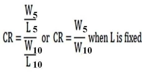
IJAEEE ,Volume 2 , Number 2
                                                                                       Rahul Garg et al.

Recent surveys indicate that roughly 30% of the worldwide semiconductor business is due to memory
chips [7-9]. Over the years, technology advances have been driven by memory designs of higher and
higher density. Electronic memory capacity in digital systems ranges from fewer than 100 bits for a
simple function to standalone chips containing 256 Mb (1 Mb _ 210 bits) or more.1 Circuit designers
usually speak of memory capacities in terms of bits, since a separate flip-flop or other similar circuit
is used to store each bit. On the other hand, system designer’s usually state memory capacities in
terms of bytes (8 bits); each byte represents a single alphanumeric character [10-12]. Very large
scientific computing systems often have memory capacity stated in terms of words (32 to 128 bits).
Each byte or word is stored in a particular location that is identified by a unique numeric address.
Memory storage capacity is usually stated in units of kilobytes (K bytes) or megabytes (M bytes).
Because memory addressing is based on binary codes, capacities that are integral powers of 2 are
most common. Thus the convention is that, for example, 1K byte 1,024 bytes and 64K bytes _ 65,536
bytes. In most memory systems, only a single byte or word at a single address is stored or retrieved
during each cycle of memory operation. Dual-port memories are also available that have the ability to
read/write two words in one cycle [2-4].

II. PROPOSED DESIGN OF 6-T FAST RAM

The schematic of Read circuitry used in the proposed design is shown in Fig-1. Read enable (RE)
signal is given as common input to two NAND gate while BL and BLbar becomes other two inputs
for the gate. Push pull configuration of transistors finally drive the Data input line. Basic NAND gate
design strategy is used to design transistors. All the transistors of the NAND gate has common W/L
ratio. Transistors M9 and M10 have twice the width of Transistor M3 and M4.

Write circuit should be able to force the BL and BLbar line to change its state as per the given input
data by charging the large bit line capacitances instantaneously. Hence write circuit is designed with
NOR gates to provide higher current driving capability. Transistor level schematic is shown in Fig-2.
The circuit resembles the read circuit with NAND gate replaced by NOR gates. Write enable (WE)
signals control the write operation. Output of each NAND gate is driven by NMOS transistor having
higher W/L ratio. These two transistors drive BL and BLbar lines.

ISSN: 2319-1112 /V2N2:317-325 ©IJAEEE
319
                                                   V2
 Design of 6-T SRAM Cell for enhanced read/write margin5Vdc

                                               M2N6851                         0                    DSTM5
                                                              M8                                         CLK
                                                                                                               READ ENABLE
                                                  M7                M2N6851
                                         BL                                                         OFFTIME = .5uS
                                                                                                    ONTIME = .5uS
                                                                                                    DELAY =
                                                                                        V4
                                                                                                    STARTVAL = 0
                                                         M1                                         OPPVAL = 1
                      V3                                                                 5Vdc   0
               5Vdc        0                                                  M2N6851
                                                  M2N6660

                               M12                                                 M9
                               M2N6851                   M2
     M2N6851
                                                                                                DATA OUT
                                                  M2N6660
        M11                                                                        M3
BL                                                             0
                                                                              M2N6660
                                                                     5Vdc
               M5                                                    V1
                                                          0
                                                                                         0
                                                          M2N6851
          M2N6660

                                                              M10
                      M6 M2N6660
                                   DSTM2
                                         CLK
                                                              M4
                                   OFFTIME = .5uS
                                   ONTIME = .5uS
                                                          M2N6660
                                   DELAY =
                      0            STARTVAL = 0
                                   OPPVAL = 1
                                                                      0
                               READ ENABLE

                                                              Fig-1 Read Circuit

 ISSN: 2319-1112 /V2N2:317-325 ©IJAEEE
IJAEEE ,Volume 2 , Number 2
Rahul Garg et al.
VDD
M2N6851 V1 0
1.8Vdc
M1
0 M2N6851
VDD 1.8Vdc BL
V2
M2 M7
OFFTIME = .5uSDSTM1 M2N6851 M2N7000
ONTIME = .5uS CLK
DELAY = 2ns
STARTVAL = 0 M3 M5 M6
OPPVAL = 1 0
M4 M2N7000 M2N7000
WRITE ENABLE M2N6851
0
BL
M10
M2N7000
M8
M2N7000 M2N7000 0
M9
0 DATA IN
Fig-2 Write Circuit
A. Row Decoder
In the case of row decoder, PMOS is activated by precharge control signal PEbar prior to the
address decoding process. All word line (WL) is pulled high to VDD during precharge. Column (or
block) decoders have to provide the discharge path from the precharged bit line to the sense amplifier
during read operation. The same lines should be able to drive the bit line to write either 0 or 1 to the
memory SRAM cell. Read and write access time of the memory is primarily restricted by the
propagation delay of the decoder. Decoder outputs are connected throughout the memory cell making
long interconnections which are main resources of delay and higher power consumption. A 2:4 row
decoder used in this design is shown in Fig-3.
ISSN: 2319-1112 /V2N2:317-325 ©IJAEEE321
Design of 6-T SRAM Cell for enhanced read/write margin
In this design MSB of Row address controls enable of sense amplifiers. When MSB=0, first row of
sense amplifiers will be enabled during read operation. Similarly when MSB=1, other row of sense
amplifiers will be enabled during read operation.
M18
M2N6851
v dd
M2N6851 U1
A1
VDDGND
en M16 I1 OUT AObA1
I2
A0
and gate
M14 U2
VDDGND
I1 OUT A0A1b
M2N6660 I2
and gate
U3
VDDGND
I1 OUT A0bA1b
M2N6851 I2
and gate
M17 U4
VDDGND
I1 OUT A0A1
M1 I2
and gate
M2N6660
gnd
Fig-3: 2:4 Decoder
B. 6-T CELL
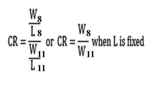
To ensure read stability of the 6T cell shown below in Fig-4, the voltage across M8 should be less
than the threshold voltage when the charge on BLBAR is discharged through M8 and M11.
Intuitively, read stability can be met by choose the size of M8 to be greater M11. The exact size of
M8 can be determined from the cell ratio (CR), where
ISSN: 2319-1112 /V2N2:317-325 ©IJAEEEIJAEEE ,Volume 2 , Number 2
Rahul Garg et al.
CR has to be greater than 1.2 to ensure read stability. A CR value of 1.5 is chosen for the design of
6T cell.
BB
BL
M2N6851
WL
VDD
M4
M2N6851
M5
M11 M9 M10
M2N6660 M2N6660
M2N6660
M2N6660
M8
GND
Fig-4 6-T SRAM Cell
To ensure write stability, the voltage across M10 should be less than the threshold voltage when
BL is pulled low to write a ‘0’ into the 6T cell. Similarly to read stability, the exact size of M10 can
be determined from the pull-up ratio (PR), where
CR has to be at least less than 1.8 to ensure read stability. A CR value of 1 is chosen for the design
of 6T cell. The end result of transistor sizing after stability analysis is shown below:
W4 = W5 = W10 = W11 minimum layout width = 0.48µm
W8 = W9 = 1.5W5 = 0.72µm
C. SENSE AMPLIFIER
Since SRAM cells provide true differential outputs any differential configuration of sense
amplifier is directly applied to SRAM design. The Schematic of latch based type of configuration
ISSN: 2319-1112 /V2N2:317-325 ©IJAEEE323
Design of 6-T
T SRAM Cell for enhanced read/write margin
used in this design is shown in Figure-5.
Figure Sense enable (SE) signal is used to turn ON/OFF,
ON/OFF the sense
amplifier BL and BLbar becomes I/O terminals of amplifier. During read operation, if cell had stored
1, then a small +ve
ve voltage will develop between BL and BLbar with VBL>VBLbar. Then amplifier
raises voltage VBL to VDD and VBLbar to 0V. This output is then directed to the chip I/O pin by the
column decoder.
M6
M2N6851 v dd
M2N6851
M7
BB BL
M2N6660 M13
M12
M2N6660
M14
s_en
M2N6660
gnd
Figure-5 Latch based Sense Amplifier
III. SIMULATION RESULTS
The read time of the design given below is compared with the proposed design. The simulation result
of the proposed design is shown below in Fig 6 (a) and (b).
WRITE ‘1’ WRIT
WRITE’0’
WRITE TIME = 45 ns
(a)
ISSN: 2319-1112 /V2N2:317-325 ©IJAEEEIJAEEE ,Volume 2 , Number 2
Rahul Garg et al.
SENSE _EN
READ ‘1’
READ TIME = 78 ns
(b)
Figure -6 Output Waveforms of 1-bit SRAM
IV. CONCLUSION
A 4×2 bits SRAM was designed and simulated in 22µm
m CMOS technology using Cadence ORCAD
16.3 software.. The simulation results indicate that the proposed design of SRAM circuit has less Read
Access Time compared to the conventional SRAM circuit. The read access
acce time in the proposed
design was 52ns which is reduced by around 34%.
This shows that the proposed design can be very effective for the applications which needed high
speed SRAMs like Cache Memory but with the cost of area. However, use of extra sense
sen amplifiers in the
proposed design do not increase the power consumption as only one sense amplifier in each column is
active during the Read operation which is controlled by Row Address of MSB. The Read Access Time
can be further reduced by considering some design modifications in Sense Amplifier which was left
untouched in this design.
V. FUTURE WORK
As the simulation results shows that the Read Access time was not reduced up to expectation, there
is much more left to do with the design in future like design of Sense amplifier for Fast Read
operation.
ISSN: 2319-1112 /V2N2:317-325 ©IJAEEE325 Design of 6-T SRAM Cell for enhanced read/write margin Also the design and Simulation was done in 2 µm technology which would have done at sub-micron level using more advanced tools but it was not possible due to the unavailability of the needed tools. So, the preferred task in future is to test the proposed design with 32KB SRAM at 32 nm Technology. REFERENCES [1] Andrew Carlson, Sriram Balasubramanian, Radu Zlatanovici, Tsu-Jae King Liu, and Borivoje Nikolic´, “SRAM Read/Write Margin Enhancements Using FinFETs”, IEEE Transactions on VLSI systems, September, 2009. [2] S. A. Tawfik and V. Kursun, “Low power and roubst 7T dual-Vt SRAM circuit”, in Proc. IEEE Int. Symp. Circ. Sys., ISCAS 2008, Seatle, WA, USA, 2008, pp. 1452–1455. [3] M. Pelgrom, A. Duinmaijer, and A. Welbers, “Matching properties of MOS transistors,” IEEE J. Solid-State Circuits, vol. 24, no. 5, pp.1433–1440, Oct. 1989. [4] H. Pilo, J. Barwin, G. Braceras, C. Browning, S. Burns, J. Gabric, S.Lamphier, M. Miller, A. Roberts, and F. Towler, “An SRAM design in 65 nm and 45 nm technology nodes featuring read and write-assist circuits to expand operating voltage,” in Proc. VLSI Circuits Symp., 2006, pp. 15–16. [5] K. Zhang, U. Bhattacharya, Z. Chen, F. Hamzaoglu, D. Murray, N.Vallepalli, Y. Wang, B. Zheng, and M. Bohr, “A 3 GHz 70 Mb SRAM in 65 nm CMOS technology with integrated column-based dynamic power supply,” in Proc. ISSCC, 2005, pp. 474–5. [6] J. P. Colinge, “Reduction of floating substrate effect in thin-film SOI MOSFETs,” Electron. Lett., vol. 22, pp. 187–188, 1986. [7] Seevinck, F.J. List, J. Lohstroh, Static-noise margin analysis of MOS SRAM cells. IEEE J. Solid-State Circuits SC-22(5), 748–754 (1987) [8] M. Sharifkhani, M. Sachdev, \ SRAM Cell Data Stability: A Dynamic Perspective", IEEE Journal of Solid State Circuits (IEEE JSSC), June 2006. [9] M. Sharifkhani, S. M. Jahinnuzaman, M. Sachdev, \ Dynamic Data Stability in SRAM Cells and its Implications on Data Stability Tests", Proceedings of IEEE International Workshop on Memory Technology, Design, and Testing, pp. 55-61, 2006 (IEEE MTDT'06). [10] J. Lohstroh, \Static and dynamic noise margins of logic circuits," IEEE J. Solid-State Circuits, vol. SC-14, pp. 591-598, 1979. [11] C. Mead and L. Conway, Introduction to VLSI systems. Addison Wesley, 1980. [12] K. Zhang, U. Bhattacharya, Z. Chen, F. Hamzaoglu, D. Murray, N. Vallepalli, Y. Yang, B.Zheng, and M. Bohr, “A SRAM Design on 65nm CMOS Technology with Integrated Leakage Scheme,” Symposium on VLSI Circuits (VLSI) Digest of Technical Papers, pp. 294-295, 2004 ISSN: 2319-1112 /V2N2:317-325 ©IJAEEE
You can also read