Development of rotational maze-shaped RF magnetron plasma for successful target utilization and thin-film preparation - IOPscience
←
→
Page content transcription
If your browser does not render page correctly, please read the page content below
Japanese Journal of Applied
Physics

REGULAR PAPER

Development of rotational maze-shaped RF magnetron plasma for
successful target utilization and thin-film preparation
To cite this article: Yasunori Ohtsu et al 2021 Jpn. J. Appl. Phys. 60 SAAB01

View the article online for updates and enhancements.

                               This content was downloaded from IP address 46.4.80.155 on 21/12/2020 at 10:06
Japanese Journal of Applied Physics 60, SAAB01 (2021)                                                                        REGULAR PAPER
https://doi.org/10.35848/1347-4065/abb758

Development of rotational maze-shaped RF magnetron plasma for successful
target utilization and thin-film preparation
Yasunori Ohtsu*, Rei Tanaka, and Takahiro Nakashima
Department of Electrical and Electronic Engineering, Saga University, 1 Honjo-machi, Saga 840-8502, Japan
*
E-mail: ohtsuy@cc.saga-u.ac.jp
Received March 24, 2020; revised April 23, 2020; accepted September 10, 2020; published online October 16, 2020

    A rotational maze-shaped RF magnetron sputtering plasma has been developed by combining three kinds of rod magnets for improving target
    utilization. The maze-shaped plasma is produced to perform the closed form along the magnetron motion predicted by the magnet arrangement.
    The radial profile of a copper target erosion has two peaks and the pattern is based on rotating the maze-shaped plasma. A target utilization rate
    has attained approximately 64.8%, which is to two to three times higher than that of conventional stable magnetron sputtering. Al-doped ZnO
    deposited thin films have shown resistivity of 1.5–2.6 × 10⁻⁴ Ω cm under a substrate at room temperature and the transmittance gets to
    approximately 90% in the visible region. It is found from X-ray diffraction pattern that the diffraction peak of AZO films is 33.97° and the grains
    exhibit a preferential orientation along the (002) axis. © 2020 The Japan Society of Applied Physics

                                                                               and AZO thin-film preparation has also been tried for
1. Introduction                                                                evaluating the rotational magnetron plasma from the view-
A physical vapor deposition (PVD) process is a practical                       point of the film quality. To produce the maze-shaped
technique for an attractive thin-film synthesis in several                      magnetized plasma, a special arrangement of neodymium
microelectronics industries. Sputtering is the most popular                    magnets is placed on an iron yoke disk. Next, magnetic field
deposition method utilized in some PVD processes. In                           simulations and the erosion depth profile are discussed for
particular, a planar magnetron sputtering plasma1–9) has                       investigating the target utilization. The deposited AZO films
been extensively utilized for preparing functional thin films                   are evaluated for their resistivity, transparency and crystalline
in various research fields. Magnetron sputtering plasma can                     property.
effectively prepare high-quality oxide films such as alu-
minum zinc oxide (AZO),10–17) indium tin oxide (ITO)18–24)                     2. Experimental procedure
and nitride films.25–29) For a transparent conductive oxide                     Figure 1 shows the experimental apparatus for the rotational
(TCO) film, it is well known12) that the radial profile of the                   maze-shaped RF magnetron plasma sputtering source. The
resistivity of AZO thin film deposited by conventional                          maze-shaped magnets arranged on an iron disk 150 mm in
magnetron sputtering exhibits a significant spatial distribu-                   diameter, shown in Fig. 2, were placed in close proximity to
tion at substrate temperature below 573 K. Namely, it is                       the target surface, as shown in Fig. 1. The target was set on
difficult to prepare the practical TCO film on flexible and                       the top flange across an insulated ring with a hole diameter of
low-melting substrates such as a plastic sheet using conven-                   100 mm and a thickness of 5 mm in the stainless-steel
tional magnetron sputtering.                                                   vacuum chamber 160 mm in diameter and 195 mm in length.
   In the magnetron plasma,1–9) the high-density plasma with a                 A copper target (overall size, 140 mm × 140 mm; sputtering
density of 1011–1012 cm−3 is achieved by the closed E × B                      diameter, 100 mm) was used for the target erosion depth
drift motion, where E and B are the electric field perpendicular                experiment. The top part of the reactor vessel above the target
and magnetic field parallel to the target, respectively.                        was held under atmospheric pressure. The vacuum chamber
However, the target material is utilized uneconomically and                    was evacuated to a pressure less than 10−4 Pa. An RF power
the erosion causes a lower target utilization of about 20%–30%                 of 20 ∼ 40 W at the driving frequency of 13.56 MHz was
of the entire target material by the end of the target life because            input to the target through a blocking capacitor of 300 pF and
the plasma is produced in a ring- or racetrack-shaped magnetic                 a matching network with an inductor and two variable
field loop ascribed by the E × B drift motion. Thus, expensive                  capacitors. The RF applied voltage ranges from 292 ∼ 456
materials and rare metals such as ITO, which includes indium,                  Vpp (peak-to-peak value) and the self-biased voltage is
are extravagantly disposed. From the viewpoint of saving                       changed from −40 ∼ −175 V. Ar gas pressure of 2 Pa, which
resources, the best solution is for the sputtering target to be                was higher than the conventional working pressure of less
fully used. In order to achieve this purpose, various approaches               than 1 Pa, was introduced into the vacuum chamber because
introducing a rotational target,30) gyratory magnets31–33) and                 the magnetic flux density on the target surface in this study is
static magnet arrangement34) have been investigated in pre-                    lower than that in conventional magnetron plasma. The iron
vious works. In these studies, the target utilization rate for                 disk holding the magnets was rotated at the rotational speed
various types of rotational plasma sputtering has attained a                   of 40 rpm by an external motor insulated by a plastic rod with
value higher than 50%. Therefore, rotational plasma sputtering                 an iron yoke. For preparing AZO film, the target was a
is the most effective method to solve the target utilization                   sintered circular plate 100 mm in diameter and 3 mm in
problem. On the other hand, the evaluation of thin-film                         thickness, made from a mixture of powered ZnO and Al2O3;
property deposited by the rotational plasma sputtering source                  the Al2O3 dopant content was 2.0 wt%. The substrate holder
has hardly been discussed.                                                     100 mm in diameter was mounted facing the target. A glass
   In this paper, we have developed rotational maze-shaped                     plate (Corning Eagle XG, 100 mm × 15 mm × 0.7 mm) was
RF magnetron sputtering plasma for higher target utilization                   mounted on the grounded substrate holder at z = 50 mm, as
                                                                       SAAB01-1                        © 2020 The Japan Society of Applied Physics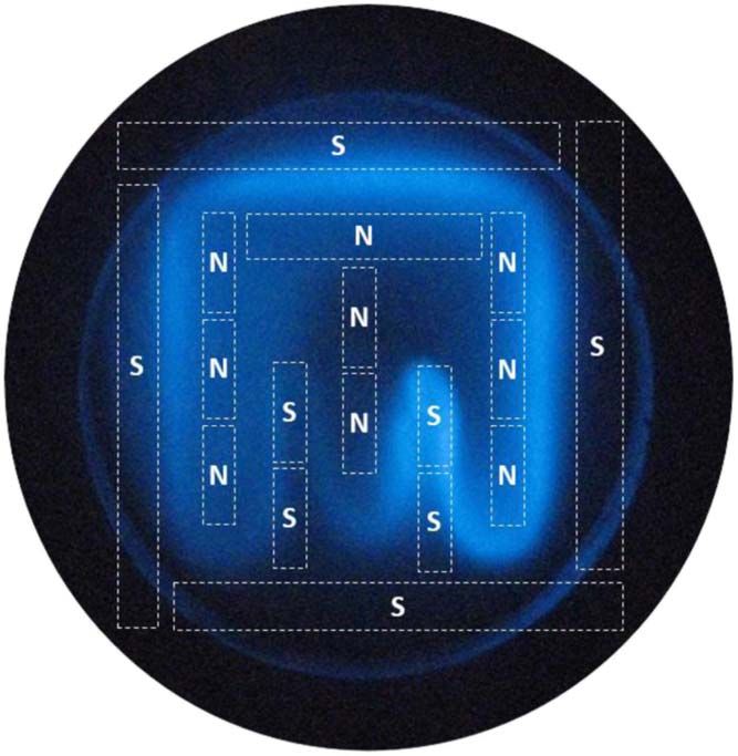
Jpn. J. Appl. Phys. 60, SAAB01 (2021)                                                                                              Y. Ohtsu et al.

         Fig. 1. (Color online) Schematic diagram of experimental apparatus for the proposed rotational maze-shaped RF magnetron plasma.

                                                                           visible near infrared (UV-NIR) spectrometer, respectively.
                                                                           The X-ray diffraction (XRD) method using Cu Kα radiation
                                                                           scanning electron microscopy (SEM) was used to analyze the
                                                                           structural property.

                                                                           3. Results and discussion
                                                                           3.1. Magnetic field simulation of the maze-shaped
                                                                           magnet arrangement and the plasma emission
                                                                           The magnetic field profile of the maze-shaped magnet
                                                                           arrangement, as shown in Fig. 2, was analyzed by a
                                                                           commercial 3D electromagnetic field simulator Femtet
                                                                           (Murata Software). In order to design the maze-shaped
                                                                           magnet arrangement, three neodymium rod magnets
                                                                           (a) 20 mm × 5 mm × 5 mm and the surface magnetic flux
Fig. 2. (Color online) Maze-shaped arrangement of three kinds of
                                                                           density, 406 mT, (b) 40 mm × 10 mm × 5 mm and 308 mT
neodymium magnets on the iron disk.
                                                                           and (c) 90 mm × 12 mm × 5 mm and 269 mT, as shown in
shown in Fig. 1 and the sputtering time was fixed at 1 h. The               Fig. 2, were set on the iron disk 150 mm in diameter. Here,
resistivity and transmittance of the deposited film were                    the origin of the x and y coordinates inserted in Fig. 2 is the
measured by the four-point probe method and ultraviolet                    center of the iron disk, while the origin of the z component is

     Fig. 3. (Color online) Top view of simulated magnetic flux density distribution of the maze-shaped magnet arrangement, as shown in Fig. 2.

                                                                   SAAB01-2                        © 2020 The Japan Society of Applied Physics
Jpn. J. Appl. Phys. 60, SAAB01 (2021)                                                                                                          Y. Ohtsu et al.

the center of the target surface and the directions of their                      maze-shaped magnet arrangement, as predicted from Fig. 2.
coordinates are defined, as shown in Fig. 2. When the RF                           It is found that the value becomes higher between the
voltage is applied to the target, a time-averaged electric field                   magnets.
E is generated to the −z axis direction perpendicular to the                         Figures 4(a) and 4(b) show the y axis profile of the
iron disk surface, as shown in Fig. 2.                                            absolute value of magnetic flux density at x = 0 and
   Figure 3 shows a top view profile of the magnetic flux                           z = 5 mm corresponding to the target surface and x axis
density on the maze-shaped magnet arrangement shown in                            profile of the absolute value of magnetic flux density at y = 0
Fig. 2. Here, the magnetic flux density denotes the value on                       and z = 5 mm, respectively. Their profile positions are shown
the magnets. The magnetic flux density is obtained along the                       as dashed lines in the insets of Figs. 4(a) and 4(b). Here, Bx,

Fig. 4. (Color online) (a) Absolute value of magnetic flux density as a function of y axis distance from the center at x = 0 and z = 5 mm. Dashed line in the
inset is the simulated y axis profile position. (b) Absolute value of magnetic flux density as a function of x axis distance from the center at y = 0 and z = 5 mm.
Dashed line in the inset is the simulated x axis profile position.

                                                                         SAAB01-3                           © 2020 The Japan Society of Applied Physics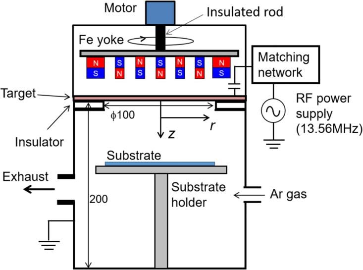
Jpn. J. Appl. Phys. 60, SAAB01 (2021)                                                                                              Y. Ohtsu et al.

                                                                        magnetron plasma is not an unbalanced magnetron because Bz
                                                                        at the edge of the substrate holder was around 0.6 mT.
                                                                           Figure 5 shows a plasma emission image of the static
                                                                        maze-shaped magnetron plasma produced at RF power of
                                                                        40 W and Ar gas pressure of 2 Pa. The image was observed
                                                                        with a commercial digital camera through an Ar interference
                                                                        filter of 488 nm. Here, the positions of the magnets are
                                                                        indicated by the dashed lines. As shown by the above
                                                                        magnetic field distributions, the maze-shaped RF magnetron
                                                                        plasma profile can be seen along the closed magnetron
                                                                        motion. It seems that the magnetron plasma emission is
                                                                        closed as the maze.
                                                                        3.2. Target erosion profile of the rotational maze-
                                                                        shaped RF magnetron sputtering plasma
                                                                        In order to evaluate the target utilization rate of the proposed
                                                                        maze-shaped RF magnetron sputtering plasma, the erosion
                                                                        experiment was examined by rotating the maze-shaped RF
                                                                        magnetron sputtering plasma shown in Fig. 5 at a rotation
                                                                        number Nr of 40 rpm, RF power PRF of 40 W, Ar gas pressure
                                                                        pAr of 2 Pa and sputtering time Tsp of 1 h. The RF applied
                                                                        voltage and self-biased voltage were 456 Vpp and −175 V,
Fig. 5. (Color online) Optical emission image of the maze-shaped RF
                                                                        respectively. Here, a copper plate 140 mm × 140 mm × 3 mm
magnetron plasma detected through an Ar interference filter (488 nm).    was used as the erosion target material to shorten the sputtering
Dashed rectangular shapes denote the arranged magnets.                  time because the sputtering yield of the copper has a higher
                                                                        value of approximately 1.2 at an incident ion energy of
By and Bz denote magnetic flux densities in the x, y and z               200 eV.35) The erosion depth of the copper plate was measured
components, respectively. In Fig. 4(a), it is found that By             by a surface roughness tester with a spatial resolution of
parallel to the target has 10 ∼ 14 mT at −40 < y < −20 mm               approximately 50 nm. Figure 6 shows the radial profile of the
and 25 ∼ 29 mT at 30 < y < 40 mm, whereas Bx parallel to                copper target erosion depth de. It is found that de has two peaks
the target is hardly observed, as expected from the setup of            of approximately 1.7 and 2.2 μm at r = 10 and 35 mm,
the magnets. Thus, the value of By is enough to magnetize               respectively. The reason the erosion profile has two peaks is
electrons because the gyro-radius of the electrons is estimated         understood by two circles of Ar emission image in the maze-
at 0.2 ∼ 0.5 mm with the assumption of electron temperature             shaped RF magnetron sputtering plasma, as shown in Fig. 7 (the
of 4 eV.33,34) Although Bz perpendicular to the target has a            same image as Fig. 5). Two dashed circles at a radius of 10 and
maximum value of 32 mT at y = 23 mm, it does not                        35 mm are added in Fig. 7. That is, a strong emission whose
contribute a magnetron motion, that is, E × B drift effect              strength is related to the plasma density is detected along the
for charged particles, because Bz is parallel to E. It can be           two dashed circles. The emission in the area between the two
seen in Fig. 4(b) that all components of the magnetic flux               dashed circles is weaker than that of the two dashed circles, so
density are almost asymmetrical to the x axis as expected               that the erosion depth has a valley at r = 25 mm. The center and
from the magnet configuration. as shown in Fig. 2. Bx has                edge areas show a lower emission than the other area.
three peaks of 10, 7.2 and 21.3 mT at x = ±6, ±19 and                      Since the diameter of the target facing the plasma is
±36 mm, respectively. Although By indicates around 8 ∼ 9                100 mm, r = 50 mm corresponds to the target edge. The
mT at −15 < x < 15 mm, the E × B drift motion does not                  erosion depth decreases drastically from 1.2 to 0.5 μm with
affect the maze-shaped E × B drift motion, as the solid lines
with arrows show in the magnet arrangement insets in
Figs. 4(a) and 4(b). As mentioned above, Bz does not
influence the magnetron motion, whereas the profile has a
unique distribution. The electron Hall parameter, which is the
ratio of electron cyclotron angular frequency to electron-
neutral collision frequency is higher than 30, so that their
distributions of the magnetic flux densities Bx and By suggest
that the magnetron motion is realized along the maze-shaped
E × B drift, as imagined in Fig. 2.
   On the other hand, the magnetic flux density on the
substrate holder at z = 50 mm was less than 0.7 mT where
the electron gyro-radius and Hall parameter were approxi-
mately 10 mm and 3, respectively. Here, the electron tempera-
ture is assumed at 2 eV33,34) for electron thermal velocity for         Fig. 6. Radial profile of the copper target erosion depth at RF power of
these calculations. It is difficult for the magnetic field on the         40 W, Ar gas pressure of 2 Pa, rotation number of 40 rpm and sputtering time
substrate holder to affect the plasma profile. The proposed              of 1 h.

                                                                   SAAB01-4                     © 2020 The Japan Society of Applied Physics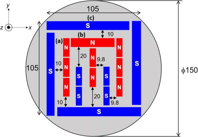
Jpn. J. Appl. Phys. 60, SAAB01 (2021)                                                                                                  Y. Ohtsu et al.

                                                                             Fig. 8. Radial profile of the resistivity of deposited AZO thin film at RF
                                                                             power of 40 W, Ar gas pressure of 2 Pa, rotation number of 40 rpm and
                                                                             sputtering time of 1 h.

Fig. 7. (Color online) Optical emission image of the maze-shaped RF
magnetron plasma on the circular target area. Two dashed circles denote
positions on the circumferences with radii of 10 and 35 mm.

increasing radial position r from 45 to 50 mm and has the
lowest value of 0.5 μm at the target edge. This is because the
electric potential of the target edge wall is floating and then
the ion sheath is formed near the target edge where the ion
sheath thickness is estimated at approximately 5 mm.
   The target utilization rate UT is calculated from the
following equation:
                        rT
                                                                             Fig. 9. Transmittance curve of AZO thin film deposited on the glass plate

             UT
                   ò
                  = 0
                             2prd e (r ) dr
                                              ´ 100%,                 (1 )
                                                                             at RF power of 40 W, Ar gas pressure of 2 Pa, rotation number of 40 rpm and
                                                                             sputtering time of 1 h.
                             prT2 d em
where rT and dem denote the target radius and maximum                        1–2.3 × 10⁻⁴ Ω cm can be produced by rotating our system
target erosion depth, respectively. Here, rT and dem are                     at substrate room temperature, whereas the resistivity of AZO
50 mm and 2.2 μm, estimated by the target erosion profile                     films deposited by conventional RF magnetron sputtering at
shown in Fig. 6, respectively. Thus, UT is estimated at                      substrate temperatures below 573 K have exhibited signifi-
approximately 64.8% using Eq. (1). The value is two to three                 cant spatial distribution.12) The result shows that rotational
times higher than that examined by the conventional static                   maze-shaped magnetron plasma sputtering is effective to
magnetron sputtering deposition.1–9) Namely, it is confirmed                  prepare the TCO thin film with uniform profile of good
that the rotational maze-shaped RF magnetron plasma is                       resistivity for the lower-melting materials under substrate
effective for improving the target utilization.                              room temperature.
3.3. Deposition of AZO thin films by rotational maze-                           The transmission spectra of AZO thin film deposited at
shaped RF magnetron sputtering plasma under non-                             0 < r < 50 mm is measured in the wavelength range from
heated substrate                                                             300–2500 nm by a UV-NIR spectrometer, as shown in Fig. 9.
AZO thin films have been deposited by rotating the maze-                      The film thickness of the AZO sample is approximately
shaped RF magnetron sputtering plasma at a rotation number                   100 nm. The transmittance is above 85% in the wavelength
Nr of 40 rpm, Ar gas pressure pAr of 2 Pa, RF power PRF of                   range from 380–780 nm. The average transmittance in the
20 W and sputtering time Tsp of 1 h. The substrate, a non-                   visible region is approximately 90%, which satisfies the
heated glass plate, was positioned at a distance z = 50 mm                   required value for transparent conductive oxide films.10–12)
from the target. The applied RF voltage and self-biased                         The XRD pattern of the AZO films is shown in Fig. 10. It
voltage were 292 Vpp and −40 V, respectively. The deposi-                    can be seen that the sharp peak is at 33.97° corresponding to
tion rate was approximately 2.5 nm min−1, which corre-                       (002). That is, the AZO films have an obvious c-axis
sponded to half of the value deposited by conventional                       orientation. Figure 11 shows a SEM image of the AZO
magnetron sputtering.1–9) Figure 8 shows resistivity ρ of                    thin-film cross-section. It is confirmed that AZO thin films
the AZO thin film as a function of radial position r. It should               have a columnar construction along the c-axis. The peak
be noted that large-area AZO with a resistivity of                           location of standard powder ZnO crystal is 34.47°.36) It is
                                                                     SAAB01-5                        © 2020 The Japan Society of Applied Physics
Jpn. J. Appl. Phys. 60, SAAB01 (2021) Y. Ohtsu et al.
Fig. 10. XRD pattern of AZO thin film deposited on the glass plate at RF power of 40 W, Ar gas pressure of 2 Pa, rotation number of 40 rpm and sputtering
time of 1 h.
substrate. The transmittance was obtained at 90% in the visible
region. The grains exhibit a preferential orientation along the
(002) axis and the XRD peak of the AZO films was 33.97°.
Acknowledgments
The work was supported by JSPS KAKENHI (Grant Nos.
JP16K05634 and JP19K03784).
1) J. Musil, Vacuum 50, 363 (1998).
2) B. Window, Surf. Coat. Technol. 81, 92 (1996).
3) P. J. Kelly and R. D. Arnell, Vacuum 56, 159 (2000).
4) M. Novotny, J. Bulir, P. Pokorny, J. Lancok, L. Fekete, J. Musil, and
M. Cekada, Surf. Coat. Technol. 228, S466 (2013).
5) B. A. Shedden, I. V. Katardjiev, S. Berg, M. Samandi, and B. Window, Surf.
Coat. Technol. 116–9, 751 (1999).
6) M. Ratova, G. T. West, and P. J. Kelly, Vacuum 115, 66 (2015).
Fig. 11. SEM image of AZO thin-film cross-section at RF power of 40 W, 7) S. M. Rossnagel and J. Hopwood, Appl. Phys. Lett. 63, 3285 (1993).
Ar gas pressure of 2 Pa, rotation number of 40 rpm and sputtering time of 1 h. 8) D. Li, S. Lopez, Y. W. Chung, M. S. Wong, and W. D. Sproul, J. Vac. Sci.
Technol. A 13, 1063 (1995).
9) R. W. Lemke, S. E. Calico, and M. Collins, IEEE Trans. Plasma Sci. 25, 364
(1997).
found that the diffraction angle of the AZO (002) is identified 10) T. Minami, H. Nanto, and S. Tanaka, Appl. Phys. Lett. 41, 958 (1982).
at a lower diffraction angle compared with the value of 11) T. Minami, H. Sato, H. Nanto, and S. Tanaka, Jpn. J. Appl. Phys. 24, L781
standard ZnO powder. This is because the stress along the (1985).
T. Minami, H. Sato, H. Imamoto, and S. Tanaka, Jpn. J. Appl. Phys. 31,
horizontal direction in the AZO film is related to the position 12)
L257 (1992).
of the diffraction angle of peak (002).37) When the peak (002) 13) J.-I. Nomoto, T. Hirano, T. Miyata, and T. Minami, Thin Solid Films 520,
diffraction angle is smaller than 34.47°, the AZO films 1400 (2011).
display compressive stress. On the other hand, the films 14) C. H. Tseng, W. H. Wang, H. C. Chang, C. P. Chou, and C. Y. Hsu,
Vacuum 85, 263 (2010).
determine tensile stress when the diffraction angle is larger
15) I. Miccoli, R. Spampinato, F. Marzo, P. Prete, and N. Lovergine, Appl. Surf.
than 34.47°. Thus, these AZO films have compressive stress. Sci. 313, 418 (2014).
16) T. Sumiyama, T. Fukumoto, Y. Ohtsu, and T. Tabaru, AIP Adv. 7, 055310
4. Conclusion (2017).
17) A. Kassis, M. Saad, and F. Nounou, Bull. Mater. Sci. 40, 791 (2017).
The maze-shaped RF magnetron sputtering plasma under 18) M. Bender, J. Trube, and J. Stollenwerk, Appl. Phys. A: Mater. Sci. Process.
rotational mode has been developed for improving the target 69, 397 (1999).
utilization rate, and the AZO thin films were deposited under 19) C.-T. Lee, Q.-X. Yu, B.-T. Tang, and H.-Y. Lee, Thin Solid Films 386, 105
non-heated substrate. The maze-shaped magnet arrangement (2001).
20) D. Mergel and Z. Qiao, J. Appl. Phys. 95, 5608 (2004).
was designed by the commercial 3D electromagnetic field 21) H. Han, Y. Zoo, S. K. Bhagat, J. S. Lewis, and T. L. Alford, J. Appl. Phys.
simulator. The maze-shaped high-luminous plasma emission 102, 063710 (2007).
has proved to be the closed form as predicted by the simulated 22) S. Calnan, H. M. Upadhyaya, S. E. Dann, M. J. Thwaites, and A. N. Tiwari,
magnetic flux density profiles. The copper target utilization Thin Solid Films 515, 8500 (2007).
23) S.-M. Kim, Y.-S. Rim, M.-J. Keum, and K.-H. Kim, J. Electroceram. 23,
rate of 64.8% is attained by rotating the maze-shaped 341 (2009).
magnetron plasma sputtering. AZO films with a resistivity of 24) J. N. Jang, Y. J. Lee, Y. Jang, J. Yun, S. Yi, and M. Hong, J. Phys. D 49,
1.5 ∼ 2.6 × 10⁻⁴ Ω cm have been produced with non-heated 215303 (2016).
SAAB01-6 © 2020 The Japan Society of Applied PhysicsJpn. J. Appl. Phys. 60, SAAB01 (2021) Y. Ohtsu et al.
25) L. Hultman, G. Håkansson, U. Wahlström, J.-E. Sundgren, I. Petrov, 31) T. Iseki, Vacuum 84, 1372 (2010).
F. Adibi, and J. E. Greene, Thin Solid Films 205, 153 (1991). 32) M. A. Hossain, T. Ide, K. Ikari, and Y. Ohtsu, Vacuum 128, 219 (2016).
26) M. Akiyama, T. Harada, C.-N. Xu, K. Nonaka, and T. Watanabe, Thin Solid 33) Y. Ohtsu, S. Tsuruta, M. Akiyama, and T. Tabaru, Surf. Coat. Technol. 307,
Films 350, 85 (1999). 1134 (2016).
27) H. C. Barshilia, B. Deepthi, and K. S. Rajam, Thin Solid Films 516, 4168 34) Y. Ohtsu, M. Shigyo, M. Akiyama, and T. Tabaru, Vacuum 101, 403
(2008). (2014).
28) A. Ababneh, U. Schmid, J. Hernando, J. L. Sánchez-Rojas, and H. Seidel, 35) B. Chapman, Glow Discharge Process (Wiley, New York, 1980), p. 380.
Mater. Sci. Eng. 172, 253 (2010). 36) H.-L. Shen, H. Zhang, L.-F. Lu, F. Jiang, and C. Yang, Prog. Nat. Sci. 20, 44
29) E. Yarar, V. Hrkac, C. Zamponi, A. Piorra, L. Kienle, and E. Quandt, AIP (2010).
Adv. 6, 075115 (2016). 37) M. Chen, Z. L. Pei, C. Sun, L. S. Wen, and X. Wang, J. Cryst. Growth 220,
30) M. Wright and T. Beardow, J. Vac. Sci. Technol. A 4, 388 (1986). 254 (2000).
SAAB01-7 © 2020 The Japan Society of Applied PhysicsYou can also read