Development of Semitransparent UV Photodetector Based on PTB7-Th:PCBM Composite Using the Cost-effective Fabrication Method
←
→
Page content transcription
If your browser does not render page correctly, please read the page content below
Int. J. Electrochem. Sci., 16 (2021) Article ID: 210514, doi: 10.20964/2021.05.12

                                                                          International Journal of
                                                                          ELECTROCHEMICAL
                                                                                  SCIENCE
                                                                                 www.electrochemsci.org

Development of Semitransparent UV Photodetector Based on
PTB7-Th:PCBM Composite Using the Cost-effective Fabrication
Method
Muhammad Riaz1, Muhammad Mehran Bashir2, Khasan S. Karimov2, Jameel-Un Nabi3,
Rana Tariq Mehmood Ahmad4, Zubair Ahmad5,*, Atif Mehmood6

1
  Department of Physics, University of Okara, Okara, Punjab, 56300, Pakistan.
2
  Ghulam Ishaq Khan Institute of Engineering Sciences and Technology, Topi, District Swabi, KPK,
23640, Pakistan.
3
  University of Wah, Quaid Avenue, Wah Cantt 47040, Punjab, Pakistan
4
  Department of Electrical Engineering, Narowal Campus, University of Engineering & Technology,
Lahore, 54890, Pakistan.
5
  Qatar University Young Scientists Center (YSC), Qatar University, 2713, Doha, Qatar
6
  Department of Electrical and Computer Engineering, Sahiwal Campus, COMSATS University
Islamabad, 57000, Pakistan.
*
 E-mail: zubairtarar@qu.edu.qa

Received: 4 January 2021 / Accepted: 24 February 2021/ Published: 31 March 2021

This article presents a semitransparent ultraviolet (UV) sandwich-surface type sensor based on PTB7-
Th: PCBM composite. The ultraviolet (UV) transparency of 29% was achieved through a cost-effective
drop-cast fabrication method. The variation in UV intensity (0 to 20,000 μW/cm2) and frequency (100
Hz, 1 kHz, 10 kHz, 100 kHz, and 200 kHz) was carried out, and variation of impedance and capacitance
has been studied. After a comprehensive analysis under specific UV strength and frequency, a
considerable increase in capacitance and a significant decrease in impedance were observed. The
generation of electron-hole pair relates such findings by increasing the concentration of charges,
combined potential, and possible frequency dependence of charge mobility under UV-irradiation. The
UV sensor can be used for measuring the UV and visible light intensities. They have applications in the
field of electronics and photonics.

Keywords: UV sensor, PTB7-Th: PCBM, semitransparent, sandwich-surface type sensor

1. INTRODUCTION

        Recently, in the field of light detectors, the ultraviolet (UV) detectors are very promising due to
their advantages in missile plume detection, flame sensing, real-time measurements, environmental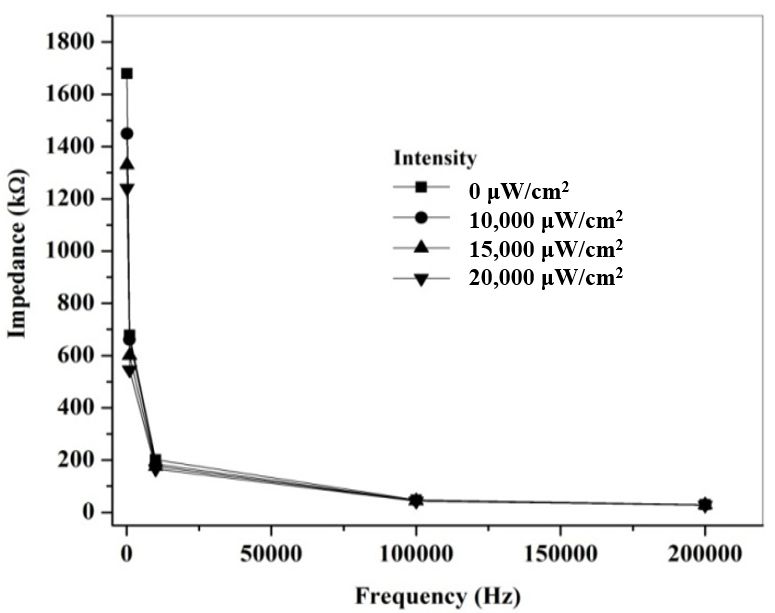
Int. J. Electrochem. Sci., 16 (2021) Article ID: 210514                                                  2

water distillation, military applications, and industrial applications. GaAs and Si-based UV sensors, due
to their quick response, are employed regardless of their poor selectivity under the spectra of the visible
and infrared region, higher cost, high vacuum, and high voltage requirement [1-5]. These disadvantages
can be overcome when organic semiconductor materials are employed for the fabrication of UV
photodetectors. Therefore, to manufacture such detectors a recently synthesized organic semiconducting
polymer poly [2, 60- 4,8 - di (5 - ethylhexylthienyl) benzo [1, 2-b; 3, 3 -b] dithiophene] [3 - fluoro - 2
[(2 - ethylhexyl) carbonyl] thieno [3, 4 - b] thiophenediyl] (PTB7-Th) is used because of its narrow-
bandgap [6]. A solar cell is manufactured with a combination of butyric acid methyl ester (PC71BM)-
[6,6] - phenyl C71[7]. The material PTB7-Th has a 1.58eV bandgap, and the absorption level lies in the
infrared region (500-585 nm). The highest occupied molecular orbital (HOMO) level of PTB7-Th
resides at 5.22eV, and the lowest unoccupied molecular orbital (LUMO)level lies at 3.64eV [8]. Fig.1
shows the schematics of PTB7-Th and PCBM. Thermally stable materials like PTB7-Th are being
investigated in different research studies for solar cell applications [9-17].
         UV detectors are manufactured with the help of organic semiconductors due to the advantages
of high sensitivity, low cost, and environment friendly. The active layers made from organic
semiconductors for UV detectors must possess high charge carrier mobility, strong absorption, and
convenient energy levels for donor and acceptor materials. In recent research studies, many UV
photodetectors based on organic semiconductor materials are developed and investigated because of
their lower cost and ease of processibility [18-29]. A new type of UV photodetector based on organic
solution-processed is introduced in [23]. An active layer of photodetector made up of poly (9,9-dioctyl
fluorenyl-2,7–yleneethynylene) (PFE) and N, N′-bis-n-butyl-1,4,5,8- naphthalenediimide (BNDI)
mixed with chloroform having a weight ratio of 3:1. The device structure made up of
ITO/PEDOT:PSS/PFE:BNDI (3 : 1)/Al measured value of 410 mA/W under 1 mW/cm2 UV light having
a voltage of −4 V at 368 nm. UV–ozone treatment is performed on a film of PEDOT: PSS to investigate
the electrical properties [24]. The application of UV-ozone treatment resulted in an increase in the
resistivity and the work function of PEDOT: PSS films. The behavior of polymer binders of organic-
based thin-film phototransistors having composition 2,7-dipenty- [1] benzothieno [2,3-b][1]
benzothiophene (C5-BTBT) with the combined effect of UV-response is investigated in [25], and the
photoelectrical properties of the C5-BTBTs are investigated. In another study, during the manufacturing
of printable transistors on a plastic substrate are investigated with the application of UV radiation along
with the response of low-temperature thermal annealing [26]. Therefore, it is concluded that during the
preparation of active layers of UV photodetector, the material should possess high mobility of charge
carriers, strong absorption ability, and should be convenient for the energy level of the donor as well as
for the acceptor materials.
         The UV sensitive devices are essential because the sunlight has 44% of visible light in the
environment at ground level, 3% of UV radiations, and the remaining in infrared radiation. Almost 77%
of UV radiations are blocked by the atmosphere. However, in space, the infrared light is about 50%,
visible light is 40%, and the remaining 10% is UV radiations; the total intensity of irradiance in a vacuum
is about 1400 W/m2. Therefore, it is useful for space technology to adopt highly sensitive UV sensitive
electronic devices.
Int. J. Electrochem. Sci., 16 (2021) Article ID: 210514 3
Moreover, it would be entirely appropriate to investigate the properties of blend PTB7-Th with
PCBM under the influence of UV irradiations. Therefore, it would be beneficial to develop solar cells
with some suitable combinations of organic semiconductor materials, which may enhance the electrical
properties. These blends of organic semiconductors can further be used for the manufacturing of UV-
based sensors. Following this motivation, we made sensors based on organic materials and investigated
their properties under the effect of UV irradiations.
This study made sensors of semitransparent PTB7-Th and PCBM blends using drop-casting,
which is quite economical technology. After that, the impedance, resistance, and capacitance were tested
under the influence of UV irradiation for the fabricated sensors.
2. EXPERIMENTAL
The materials (PTB7-Th, PCBM, Chlorobenzene, etc.) were procured from Taiwan based
company named Luminescence Technology Corporation, and these materials do not need further
purification for utilization. When the materials were received, they were placed immediately in a glove
box. The stepwise fabrication of the device is explained. At first, the solution of PTB7-Th and PCBM
(1:1.5 w/w) was mixed with chlorobenzene in a glove box, having filled with argon and was kept for 5
days. The type of solution formation method for this research was adopted from previous studies
[8,13,15-17]. After that, the solution of chlorobenzene with PTB7-Th+PCBM (35 mg/ml) was placed on
an ITO-coated glass substrate using drop-casting and was placed at room temperature for 3 hours drying.
The film's thickness was 200-210 nm for the PTB7-Th: PCBM solution and was measured with AFM as
per the ref [30]. Graphene composite was used with glue to complete the device, and the second contact
was made with this composite over the organic layer.
The molecular structure of organic materials PTB7-Th and PCBM is shown in Fig.1 [17], and
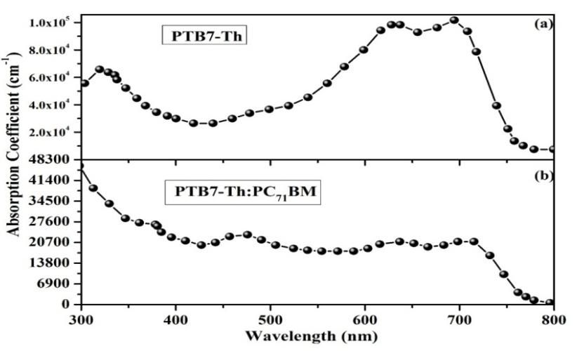
the absorption spectra of blend PTB7-Th: PCBM is shown in Fig.2 [31].
Figure 1.Schematic diagrams of the PTB7-Th and PC61BM molecules.
In Fig. 2, the top panel represents the PTB7-Th absorption, and the bottom panel represents the
PTB7-Th: PCBM absorption. The PTB7-Th absorption range is 500-785nm, and the absorption of UV-Int. J. Electrochem. Sci., 16 (2021) Article ID: 210514 4
A is 315-400nm. The addition of PCBM increases the absorption towards a shorter wavelength range
resulting in an increased absorption coefficient for PTB7-Th: PCBM blend.
Figure 2. The visible absorption spectra of PTB7-Th: PCBM blend.
The device performance was analyzed with the help of surface morphology. The Nanosurf was
used for AFM images of the prepared device. To analyze the surface morphology of PTB7-Th + PCBM
film-coated blend, AFM measurements are shown in Fig. 3. The film's top view is shown in Fig. 3(a),
and Fig. 3(b) shows the oblique view. From the results of AFM, it can be observed that the film of PTB7-
Th + PCBM is well mixed and makes a uniform layer on the substrate. The value of 30-35 nm was
recorded for the roughness of the film.
Figure 3. AFM images of the PTB7-Th and PC71BM samples (a) front view, (b) and oblique view.Int. J. Electrochem. Sci., 16 (2021) Article ID: 210514 5
Fig. 4 presents the schematic diagram of the fabricated sandwich-surface type ITO/PTB7-Th:
PCBM/Graphene composite sensor. The samples having sandwich-surface types are useful for the
optimization of the overall impedance. An increase or decrease in the values of the impedance,
resistance, or capacitance of the samples can easily be achieved by changing the surface parts of samples
and the ratio of sandwich length. In our case, the surface part lengths and sandwich of the PTB7-
Th:PCBM sensor was equal to 90% and 10%, respectively.
The measured UV transparency of the sensor was around (29-30)%. During the experiments, the
UV beam was perpendicular to the top surface of PTB7-Th:PCBM sample.
Figure 4.The schematic diagram of the fabricated device.
Figure 5. XRD pattern for PCBM powder pristine form (a) and for PTB7-Th (b)
Fig.5 shows the XRD pattern of the pristine form of PCBM and PTB7-Th powders. The PCBM
pattern shown in Fig.5a represents the two peaks at 17.50 and 20.02 degrees, and these peaks correlate
with the PCBM crystalline structure [32] due to its high level of purity, about 99.5%. The PTB7-Th
pattern is shown in Fig.5(b), representing the recorded diffraction peak at 2θ = 22.610 that correspondsInt. J. Electrochem. Sci., 16 (2021) Article ID: 210514 6
to the formation of (010) plane, which is linked with pi-pi staking having a face on orientations, with the
d-spacing value of 0.39 nm. These results are in accordance with the studies presented in [36-38].
During the experimentation, a specially designed chamber was used for the placement of
samples. Lutron UV-340 A intensity meter was used for the measurement of UV irradiation. Impedance,
resistance, and capacitance were measured using the LCR meter model MT 4090, keeping the frequency
range from 100 Hz to 200 kHz. During the experimentation, all the samples were treated at room
temperature, i.e., 25 oC. For the light source, a filament lamp was used for checking the transparency of
prepared samples in the visible spectra. The values were measured with the LM-80 Amprobe intensity
meter's help, and the recorded value was in the range of 58 to 60%.
3. RESULTS AND DISCUSSION
Fig.6 shows the impedance dependence at different frequencies of 100 Hz, 1 kHz, 10 kHz, 100
kHz, and 200 kHz of the ITO/PTB7-Th:PCBM/Graphene composite samples as a function of the
intensity of UV irradiation are shown. As the UV irradiation intensity increases up to 20,000 μW/cm2,
the impedance decreases depending on the frequency of the applied voltage during measurement. The
impedance was reduced at different values of frequencies, at 100 Hz, the decrease in value was 1.35
times, at 1 kHz 1.24 times, at 10 kHz 1.22 times, at 100 kHz 1.12 times, and at 200 kHz 1.09 times as
compared to the original value. Fig.7 the increase in capacitance values at different frequencies of
frequencies; at 100 Hz, the rise in value was 1.25 times, at 1 kHz 1.24 times, at 10 kHz 1.18 times 100
kHz 1.14 times, and at 200 kHz 1.08times than the original value. At lower frequencies, the behavior
was slightly non-linear, and at higher frequencies, the behavior was quasi-linear.
Figure 6. Variation in the impedance w.r.t UV intensity (at different frequencies)Int. J. Electrochem. Sci., 16 (2021) Article ID: 210514 7
It is well known that UV irradiation can deteriorate the structure of devices and solid and can
also change their properties. The effect of UV irradiation on the phase transition of semiconductor-metal
was studied in single-crystal vanadium dioxide [33]. Under UV light, the phase-transition temperature
in VO increased by 2 K. The UV radiation-induced the formation of clusters of the tetragonal VO phase
that persisted at temperatures below the critical one [33].
The transitions of metal-insulator in different oxides such as vanadium oxide (VO) possessed the
greater potential for scientific research and were investigated in ref. [34]. Because several oxidation
states exist, when VO films of high-quality were synthesized on the substrates. There are characteristics
of phase transition i.e., the resistance of large jumps in phase transition was observed. It was observed
that the ratio of resistance over a metal-insulator transition and the VO thin-film resistance could be
modulated with the use of UV irradiation at slightly lower temperatures. The incorporation of oxygen
due to the creation of exciting species of oxygen enabled the tunable controlled stoichiometry. The effect
of polymer binders on organic thin-film-based phototransistors having a UV-response with the
combination of benzothienobenzothiophene semiconductor was investigated in ref. [35]. UV–ozone
treatment was performed on the PEDOT:PSS films to investigate their electrical properties [39]. The
effect of UV irradiation and slightly lower temperature on the solution-processed, high-performance
TFTs and metal-oxide semiconductors was investigated in ref. [40]. In studies conducted in [33-35, 39,
40], the UV effect on the properties and structure of the organic and inorganic semiconductors and
electronic devices were also investigated. Because of UV irradiation, there exist both reversible and
irreversible processes. The reversible processes relate with the change in physical properties whereas
irreversible processes are concerned with the molecular structure. In this study, it was found that the
effect of UV irradiation increases the number of electron-hole pairs in semitransparent PTB7-Th and
PCBM sensor thereby increasing the charge concentration to change the values of impedance and
capacitance. This increased charge concentration is a reversible effect because of the low intensity of
UV irradiation.
Figure 7. Variation in the capacitance of sample w.r.t intensity of UV irradiation (at different
frequencies)Int. J. Electrochem. Sci., 16 (2021) Article ID: 210514 8
In Fig.8, it can be seen that the impedance of the ITO/PTB7-Th:PCBM/Graphene composite
samples directly relates to the frequency under the influence of different intensities of UV irradiation.
The values show that frequency and impedance are inversely related to each other. In Fig.9, it can be
observed that the capacitance of the ITO/PTB7-Th:PCBM/Graphene composite samples refers directly
to the frequency under the influence of different intensities of UV irradiation. The values show that
frequency and capacitance are inversely related to each other.
Figure 8.Variation in the impedance of the ITO/PTB7-Th:PCBM/Graphene composite samples w.r.t
frequency (at different intensities of UV irradiation)
Fig.8 and Fig.9 explain that the reactive current increases with capacitance and the active current
related to the resistance. This phenomenon is represented in the equivalent circuit of Fig.10. The
relationship between frequency and resistance was well explained and investigated in ref [41] that the
frequency directly depends on the charge mobility for higher frequencies. Therefore, charge mobility is
directly related to the frequency, and as the mobility of charges increases, the resistance decreases.
The relationship between impedance, resistance, and capacitance (concerning the equivalent
circuit shown in Fig.10) can be explained by an electric point of view [42].
Z = R /(1 + j ωRC) (1)
where ω stands for angular frequency. From Eq.1, the frequency and impedance are inversely
proportional to each other.
The term sensitivity (Sz for impedance and Sc for capacitance) plays an important role while
measuring the change in values of impedance and capacitance when the intensity of UV radiation
increases. It is determined by:
Sz= ΔZ/Int (2)
Sc = ΔC/Int (3)Int. J. Electrochem. Sci., 16 (2021) Article ID: 210514 9
where ΔZ represents the change in impedance, ΔC represents the change in capacitance and
interferes with the UV intensity. The values of the Sz were measured to be (-0.022 kΩ/(μW/cm2), (-
0.0066 kΩ/(μW/cm2), (-0.0018 kΩ/(μW/cm2), (0.00026 kΩ/(μW/cm2), (-0.00012 kΩ/(μW/cm2) at
frequencies 100 Hz, 1 kHz, 10 kHz,10 0kHz and 200 kHz, respectively.
Figure 9. Variation in the capacitance of the ITO/PTB7-Th:PCBM/Graphene composite samples w.r.t
frequency (at different intensities of UV irradiation)
The values of Sc were measured as (0.004 pF/(μW/cm2), (0.0015 pF/(μW/cm2), (0.00045
pF/(μW/cm2), (0.00015 pF/(μW/cm2), (0.0001 pF/(μW/cm2) at frequencies 100 Hz, 1 kHz, 10 kHz,100
kHz and 200 kHz, respectively. The results show that the sensitivities (Sz and Sc) decreased sharply
with increased applied frequency. This change in value is due to capacitance in Eq.1 and can also be
seen in Fig.10.
C
R
Figure 10. Equivalent circuit of the ITO/PTB7-Th:PCBM/Graphene composite sensor.
Table 1 shows the comparison of current work with previously available work in literature. In
ref. [43] the PCP was synthesized and investigated in the UV intensity bandwidth of 0-1 mW/cm2Int. J. Electrochem. Sci., 16 (2021) Article ID: 210514 10
showing a good response to UV light intensity. In ref. [24], in the same intensity region
ITO/PEDOT:PSS/CFC:ZnO/Al was investigated, which shows a better response. The Au@rGO/GaN
was investigated for UV in ref. [44], which offers an improved response to UV, also applicable for CO
gas sensing applications. But in the current work, the ITO/PTB7-Th:PCBM/Graphene composite
investigated under UV intensity bandwidth of 0-20 mW/cm2 with better reopened to UV, in vast
intensity region in comparison to other above-discussed materials.
Table 1. Comparison with literature
Structure Bandwidth Reference
ITO/PEDOT:PSS/PCP/NSN/LiF/Al/Ag 0-1 mW/cm2 [43]
ITO/PEDOT:PSS/CFC:ZnO/Al 0-1 mW/cm2 [24]
Au@rGO/GaN 0.52-1.56 mW/cm2 [44]
ITO/PTB7-Th:PCBM/Graphene 0-20 mW/cm2 Current work
composite
Sensors are being used in a variety of applications based on state-of-the-art materials having
better responses [45-50]. However, transparent and semitransparent devices are of utmost importance in
the contemporary world and are used in different areas of digital displays, solar cells, and touch screens.
In recent studies, electronic devices made up of transparent and semitransparent materials are used for
the fabrication and investigation of organic semiconductor solar cells [51], transistors [51, 53], OLEDs
[52], transparent contacts for organic devices [54], transparent lithium-ion batteries [55], and
semitransparent energy harvesting by photo-thermoelectric cells [56]. Recently, hybrid sensors were also
fabricated sensors, ultraviolet sensors, fluorescent chemo-sensors, and immune-sensors [57, 58]. The
fabrication of semitransparent PTB7-Th and PCBM sandwich-surface samples and its results are very
much beneficial for applying electronic devices and instrumentation.
4. CONCLUSIONS
This work demonstrates the fabrication of ITO/PTB7-Th:PCBM/Graphene composite
semitransparent sensors, and their electrical properties were investigated under UV radiations. The
prepared sensors were simultaneously semitransparent to visible light. The sandwich-surface type
structure introduced in this work allows one to change the sandwich's ratio and its surface parts to
increase or decrease the overall impedance. The impedance and capacitance were investigated at
different frequencies of 100 Hz, 1 kHz, 10 kHz, 100 kHz, and 200 kHz for the ITO/PTB7-
Th:PCBM/Graphene composite samples under the effect of UV irradiation showed that the UV intensity
is inversely related to the impedance and is directly related to the capacitance of the samples. As weInt. J. Electrochem. Sci., 16 (2021) Article ID: 210514 11
increase the frequency of applied voltage, the decrease in values was noted for impedance, capacitance,
and sensitivity of the UV sensor.
When the UV irradiation intensity was increased, the number of electron-hole pairs increased,
increasing the capacitance, the concentration of charges, and decreasing the sensors' impedance. The
sensors can be used for the measurement of the UV and visible light intensities. These sensors can be
used in different applications like electronic devices, instrumentation, and photonics. Because of the
fabrication of semitransparent sensors of UV and visible light, future electronics technology applications
will broaden, and these sensors will be a great addition to the family of semitransparent devices.
ACKNOWLEDGEMENTS
The authors would like to acknowledge the support of the Higher Education Commission Pakistan,
Pakistan Science Foundation, GIK Institute of Engineering Sciences and Technology of Pakistan for
providing the necessary research facilities. The authors acknowledge the support of Dr. Rashid Ali for
XRD patterns and Dr. Imran Khan for AFM images.
References
1. R.D. McKeag, S.S.M. Chan, R.B. Jackman, Appl. Phys. Lett., 67 (1995) 2117.
2. M.D. Whitfield, S.S.M. Chan, R.B. Jackman, Appl. Phys. Lett., 68 (1996) 290–292.
3. E. Monroy, F. Calle, J.L. Pau, E. Muñoz, F. Omnès, B. Beaumont, P. Gibart, J. Cryst. Growth, 230
(2001) 537–543.
4. K. Liu, M. Sakurai, M. Aono, Sensors, 10 (2010) 8604–8634.
5. K. Bayat, Y. Vygranenko, A. Sazonov, M. Farrokh-Baroughi, Semicond. Sci. Technol., 21 (2006)
1699–1702.
6. G. Li, R. Zhu, Y. Yang, Nat. Photonics, 6 (2012) 153–161.
7. F. Petraki, V. Papaefthimiou, S. Kennou, Org. Electron., 8 (2007) 522–528.
8. S.H. Liao, H.J. Jhuo, Y.S. Cheng, S.A. Chen, Adv. Mater., 25 (2013) 4766–4771.
9. J. Xiao, Z. Chen, G. Zhang, Q.Y. Li, Q. Yin, X.F. Jiang, F. Huang, Y.X. Xu, H.L. Yip, Y. Cao, J.
Mater. Chem. C, 6 (2018) 4457–4463.
10. A. Mahmood, J. Hu, A. Tang, F. Chen, X. Wang, E. Zhou, Dye. Pigment, 149 (2018) 470–474.
11. S. F. Hoefler, T. Rath, N. Pastukhova, E. Pavlica, D. Scheunemann, S. Wilken, B. Kunert, R. Resel,
M. Hobisch, S. Xiao, G. Bratina, J. Mater. Chem. A, 6(2018), 9506-9516.
12. L. Fernandes, H. Gaspar, J.P.C. Tomé, F. Figueira, G. Bernardo, Polym. Bull., 75 (2018) 515–532.
13. Z. Yin, J. Wei, S.C. Chen, D. Cai, Y. Ma, M. Wang, Q. Zheng, J. Mater. Chem. A, 5 (2017) 3888–
3899.
14. Q. Wan, X. Guo, Z. Wang, W. Li, B. Guo, W. Ma, M. Zhang, Y. Li, Adv. Funct. Mater., 26 (2016)
6635–6640.
15. S. Nam, J. Seo, S. Woo, W.H. Kim, H. Kim, D.D.C. Bradley, Y. Kim, Nat. Commun., 6 (2015) 1-9.
16. N. Li, C.J. Brabec, Energy Environ. Sci., 8 (2015) 2902–2909.
17. S.H. Liao, H.J. Jhuo, P.N. Yeh, Y.S. Cheng, Y.L. Li, Y.H. Lee, S. Sharma, S.A. Chen, Sci. Rep., 4
(2014) 1–7.
18. Z. Su, W. Li, B. Chu, T. Li, J. Zhu, G. Zhang, F. Yan, X. Li, Y. Chen, C.S. Lee, Appl. Phys. Lett., 93
(2008) 103309.
19. G. Zhang, W. Li, B. Chu, Z. Su, D. Yang, F. Yan, Y. Chen, D. Zhang, L. Han, J. Wang, H. Liu, G.
Che, Z. Zhang, Z. Hu, Org. Electron., 10 (2009) 352–356.Int. J. Electrochem. Sci., 16 (2021) Article ID: 210514 12
20. H.G. Li, G. Wu, H.Z. Chen, M. Wang, Curr. Appl. Phys., 11 (2011) 750–754.
21. Y. Han, G. Wu, M. Wang, H. Chen, Polymer, 51 (2010) 3736–3743.
22. Y.-G. Han, L.-L. Wu, J. Electron. Mater., 40 (2011) 2147–2151.
23. F. Ali, N. Periasamy, M.P. Patankar, K.L. Narasimhan, J. Phys. Chem. C,115 (2011) 2462–2469
24. H.G. Li, G. Wu, M.M. Shi, H.Z. Chen, M. Wang, Synth. Met., 160 (2010) 1648–1653.
25. F. Yan, H. Liu, W. Li, B. Chu, Z. Su, G. Zhang, Y. Chen, J. Zhu, D. Yang, J. Wang, Appl. Phys.
Lett., 95(2009) 334.
26. L. Wang, D. Zhao, Z. Su, F. Fang, B. Li, Z. Zhang, D. Shen, X. Wang, Org. Electron., 11 (2010)
1318–1322.
27. Y. Han, G. Wu, M. Wang, H. Chen, Appl. Surf. Sci., 256 (2009) 1530–1533.
28. H.G. Li, G. Wu, H.Z. Chen, M. Wang, Org. Electron., 12 (2011) 70–77.
29. J.B. Wang, W.L. Li, B. Chu, L.L. Chen, G. Zhang, Z.S. Su, Y.R. Chen, D.F. Yang, J.Z. Zhu, S.H.
Wua, F. Yan, H.H. Liu, C.S. Lee, Org. Electron., 11 (2010) 1301–1306.
30. T.H. Kim, H.I. Kwon, J.D. Lee, B.G. Park, Int. Microprocess. Nanotechnol. Conf., (2001) 240–241.
31. G. Memisoglu, C. Varlikli, Int. J. Photoenergy, 2012 (2012) 1-11.
32. C. Keiderling, S. Dimitrov, J.R. Durrant, J. Phys. Chem. C, 121 (2017) 14470–14475.
33. A. Avilov, N. Levshin, S. Poroikov, E. Revina, V. Khitrova, Crystallogr. Rep., 40 (1995) 321–323.
34. C. Ko, S. Ramanathan, J. Appl. Phys.,103 (2008) 106104.
35. D. Ljubic, C.S. Smithson, Y. Wu, S. Zhu, ACS Appl. Mater. Interfaces, 8 (2016) 3744–3754.
36. O. Amargós-Reyes, J.L. Maldonado, D. Romero-Borja, D. Barreiro-Argüelles, I. Caballero-
Quintana, O. Barbosa-García, J.A. Gaspar, J. Mater. Sci., 54 (2019) 2427–2445.
37. H.C. Liao, C.C. Ho, C.Y. Chang, M.H. Jao, S.B. Darling, W.F. Su, Mater. Today, 16 (2013) 326–
336.
38. W. Li, B. Guo, C. Chang, X. Guo, M. Zhang, Y. Li, J. Mater. Chem. A, 4 (2016) 10135–10141.
39. T. Nagata, S. Oh, T. Chikyow, Y. Wakayama, Org. Electron., 12 (2011) 279–284.
40. H. Majumdar, J. Leppäniemi, K. Ojanperä, O.H. Huttunen, A. Alastalo, Proc. 5th Electron. Syst.
Technol. Conf., (2014) 1-3.
41. P. Prins, F.C. Grozema, J.M. Schins, L.D.A. Siebbeles, Phys. Status Solidi B, 243 (2006) 382–386.
42. A. Din, K. Akhtar, K.S. Karimov, N. Fatima, A.M. Asiri, M.I. Khan, S.B. Khan, J. Mol. Liq., 237
(2017) 266–271.
43. J.L. Zhang, Y.X. Nan, H.G. Li, W.M. Qiu, X. Yang, G. Wu, H.Z. Chen, M. Wang, Sens. Actuators,
B, (2012) 321-6.
44. M. Reddeppa, S.B. Mitta, T. Chandrakalavathi, B.G. Park, G. Murali, R. Jeyalakshmi, S.G. Kim,
S.H. Park, M.D. Kim, Curr. Appl Phys., 19(2019) 938-45.
45. Li. Chuang, Li. Sun, Xu. Ziqiang, Wu. Xiangxiang, L. Tianqi, Shi. Wenlong, Int. J. Struct. Stab.
Dyn., 20 (2020) 2040011
46. M. Wang, M. Hu, B. Hu, C. Guo, Y. Song, Q. Jia, L. He, Z. Zhang, S. Fang, Biosens. Bioelectron.,
135 (2019) 22-29.
47. L. Sun, C. Li, C. Zhang, Z. Su, C. Chen, Int. J. Struct. Stab. Dyn., 08 (2018) 1840001.
48. L. Jia, B. Liu, Y. Zhao, W. Chen, D. Mou, J. Fu, Y. Wang, W. Xin, L. Zhao, J. Mater. Sci., 34
(2020) 16197-16210.
49. F. Zhang, Y. Zhou, Y. Zhang, D. Li, Z. Huang, J. Nanophotonics, 9 (2020) 568.
50. P. Xu, W. Lu, J. Zhang, L. Zhang, ACS Sustainable Chem. Eng., 33 (2020) 12366-12377.
51. A. Colsmann, A. Puetz, A. Bauer, J. Hanisch, E. Ahlswede, U. Lemmer, Adv. Energy Mater., 1
(2011) 599–603.
52. J. Meyer, S. Hamwi, M. Kröger, W. Kowalsky, T. Riedl, A. Kahn, Adv. Mater., 24 (2012) 5408–
5427.
53. G. Eda, G. Fanchini, M. Chhowalla, Nat. Nanotechnol., 3 (2008) 270–274.
54. Z. Dai, Z. Wang, X. He, X. X. Zhang, H.N. Alshareef, Adv. Funct. Mater., 41 (2017) 1703119.
55. S. Oukassi, L. Baggetto , C. Dubarry , L. Le Van-Jodin , S. Poncet, R. Salot, ACS Appl. Mater.Int. J. Electrochem. Sci., 16 (2021) Article ID: 210514 13
Interfaces, 11 (2018) 683-90.
56. M.M. Bashir, K.H. Karimov, J.U. Nabi, N. Fatima, R. Ali, Int. J. Electrochem. Sci., 14 (2019)
8544-8556.
57. S. Wang, Y. Kang, L. Wang, H. Zhang, Y. Wang, Y. Wang, Sensors Actuators, B Chem., 182 (2013)
467–481.
58. P.D. Sahare, S. Kumar, S. Kumar, F. Singh, Sens. Actuators, A, 279 (2018) 351–360.
© 2021 The Authors. Published by ESG (www.electrochemsci.org). This article is an open access article
distributed under the terms and conditions of the Creative Commons Attribution license
(http://creativecommons.org/licenses/by/4.0/).You can also read