Diamond thin films: a 21st-century material
←
→
Page content transcription
If your browser does not render page correctly, please read the page content below
Diamond thin films: a 21st-century material
                                    By Paul W. M a y
          School of Chemistry, University of Bristol, Bristol BS8 1TS, UK

Diamond has some of the most extreme physical properties of any material, yet its
practical use in science or engineering has been limited due its scarcity and expense.
With the recent development of techniques for depositing thin films of diamond on
a variety of substrate materials, we now have the ability to exploit these superlative
properties in many new and exciting applications. In this paper, we shall explain the
basic science and technology underlying the chemical vapour deposition of diamond
thin films, and show how this is leading to the development of diamond as a 21st
century engineering material.
                 Keywords: review; diamond; chemical vapour deposition;
                        thin film; hard coatings; semiconductor

                              1. The diamond in history
Probably more so than any other gemstone, diamonds feature more predominantly in
the history and cultural heritage of the human race (Ward 1998). They were prized
for their scarcity for centuries, and still remain a symbol of wealth and prestige to
this day. The word diamond comes from the Greek adamas, meaning indestructible.
Diamonds were first mined in India over 4000 years ago, but the modern diamond
era only began in 1866, when huge diamond deposits were discovered in Kimberley,
South Africa, creating a huge rush of European prospectors. The wealth this created
helped to underwrite the British Empire, and changed the fates of many African
countries.
   Apart from their appeal as gemstones, diamonds possess a remarkable range of
physical properties. Indeed, a glance at any compendium of material data proper-
ties will prove that diamond is almost always ‘the biggest and best’. A selection of
some of these properties is given in table 1. Among other properties, diamond is
the hardest known material, has the highest thermal conductivity at room temper-
ature, is transparent over a very wide wavelength range, is the stiffest material, the
least compressible, and is inert to most chemical reagents. With such a wide range of
exceptional properties, it is not surprising that diamond has sometimes been referred
to as ‘the ultimate engineering material’.
   Unfortunately, it has proved very difficult to exploit these properties, due both to
the cost and scarcity of large natural diamonds, and the fact that diamond was only
available in the form of stones or grit. It had been known for 200 years that diamond
is composed solely of carbon (Tennant 1797), and many attempts were made to
synthesize diamond artificially using as a starting material another commonly occur-
ring form of carbon, graphite. This proved extremely difficult, mainly because at
room temperature and pressure, graphite is the thermodynamically stable allotrope

Phil. Trans. R. Soc. Lond. A (2000) 358, 473–495                c 2000 The Royal Society

                                               473
474 P. W. May
Table 1. Some of the outstanding properties of diamond (Field 1992)
extreme mechanical hardness (ca. 90 GPa) and wear resistance
highest bulk modulus (1.2 × 10¹² N m−2 )
lowest compressibility (8.3 × 10⁻¹³ m2 N−1 )
highest room temperature thermal conductivity (2 × 10³ W m−1 K−1 )
thermal expansion coefficient at room temperature very low (1 × 10⁻⁶ K)
broad optical transparency from the deep ultraviolet to the far infrared
highest sound propagation velocity (17.5 km s−1 )
very good electrical insulator (room temperature resistivity is ca. 1013 Ω cm)
diamond can be doped, becoming a semiconductor with a wide bad gap of 5.4 eV
very resistant to chemical corrosion
biologically compatible
some surfaces exhibit very low or ‘negative’ electron affinity
of carbon. Although the standard enthalpies of diamond and graphite only differ by
2.9 kJ mol−1 (Bundy 1980), a large activation barrier separates the two phases pre-
venting interconversion between them at room temperature and pressure. Ironically,
this large energy barrier, which makes diamond so rare, is also responsible for its
existence, since diamond, once formed, cannot spontaneously convert to the more
stable graphite phase. Thus, diamond is said to be metastable, that is, kinetically
stable but not thermodynamically stable.
To overcome these problems, researchers realized that in order to form diamond,
conditions are needed where diamond is the more stable phase. The knowledge of
the conditions under which natural diamond is formed deep underground suggested
that diamond could be formed by heating carbon under extreme pressure. This pro-
cess forms the basis of the so-called high-pressure high-temperature (HPHT) growth
technique (Field 1992), first marketed by General Electric, and which has been used
to produce ‘industrial diamond’ for several decades. In this process, graphite is com-
pressed in a hydraulic press to tens of thousands of atmospheres, heated to over
2000 K in the presence of a suitable metal catalyst, and left until diamond crystal-
lizes. The diamond crystals this produces are used for a wide range of industrial
processes, which use the hardness and wear resistance properties of diamond, such
as cutting and machining mechanical components, and for polishing and grinding of
optics. However, the drawback of the HPHT method is that it still produces diamond
in the form of single crystals ranging in size from nanometres to millimetres, and
this limits the range of applications for which it can be used. What is required is a
method to produce diamond in a form that can allow many more of its superlative
properties to be exploited, in other words, as a diamond thin film.
2. Chemical vapour deposition
Rather than try to duplicate nature’s method for creating diamond (as in the HPHT
method), diamond could conceivably be produced if carbon atoms could be added
one-at-a-time to an initial template, in such a way that a tetrahedrally bonded car-
bon network results. If this could be accomplished from the gas phase using much
lower pressure than in HPHT, there would be an obvious advantage in terms of equip-
ment and energy costs. These ideas led to the experiments of Eversole (1958) and
Phil. Trans. R. Soc. Lond. A (2000)Diamond thin films 475
Deryagin et al . (1968), in which thermal decomposition of carbon-containing gases
under reduced pressure was used to grow diamond on the surface of natural diamond
crystals heated to 900 ◦ C. However, the rate of growth in these early experiments
was low, since graphite was co-deposited with the diamond leading to impure mixed
phases. The breakthrough came in the late 1960s, when Angus’s group discovered
that the presence of atomic hydrogen during the deposition process would lead to
preferential etching of the graphite, rather than diamond (Angus et al. 1968; Poferl
et al. 1973). Subsequent Russian work showed that such chemical vapour deposi-
tion (CVD) techniques could be used to grow diamond on non-diamond substrates
(Deryagin et al. 1976; Spitsyn et al. 1981). In 1982 Japanese researchers at the
National Institute for Research in Inorganic Materials (NIRIM) brought all these
findings together to build a ‘hot filament reactor’, which grew good quality diamond
films on non-diamond substrates at significant rates (ca. 1 µm h−1 ) (Matsumoto et
al . 1982a, b). The following year the same group reported another method for achiev-
ing diamond growth, using a microwave plasma reactor (Kamo et al. 1983; Saito et
al. 1986). This series of discoveries stimulated worldwide interest in diamond CVD,
in both academia and industry, which continues to the present day.
3. Methods for production of diamond CVD
Chemical vapour deposition, as its name implies, involves a gas phase chemical reac-
tion occurring above a solid surface, which causes deposition onto that surface. All
CVD techniques for producing diamond films require a means of activating gas phase
carbon-containing precursor molecules. This activation can involve thermal methods
(e.g. a hot filament), electric discharge (e.g. DC, RF or microwave), or a combustion
flame (such as an oxyacetylene torch). Figure 1 illustrates some of the more popular
experimental methods. While each method differs in detail, they all share a number
of features in common. For example, growth of diamond (rather than graphite) nor-
mally requires that the precursor gas (usually CH4 ) is diluted in excess of hydrogen,
in a typical mixing ratio of 1%vol. CH4 . Also, the temperature of the substrate is
usually greater than 700 ◦ C to ensure the formation of diamond rather than amor-
phous carbon. A detailed review of the various methods used for fabricating diamond
can be found in Dischler & Wild (1998), but some of the more important will be
mentioned here.
Hot filament CVD (HFCVD) (see figure 1a) uses a vacuum chamber continually
pumped using a rotary pump, while process gases are metered in at carefully con-
trolled rates (typically a total flow rate of a few hundred sccm). Throttle valves main-
tain the pressure in the chamber at typically 20–30 Torr, while a substrate heater
is used to bring the substrate up to a temperature of 700–900 ◦ C. The substrate to
be coated—e.g. a piece of Si or Mo—sits on the heater, a few millimetres beneath
a filament, which is electrically heated to temperatures in excess of 2200 ◦ C. The
filament is made from a metal that will be able to survive these conditions and not
react significantly with the process gas. Metals such as tungsten and tantalum are
most often used, although they do eventually react with the carbon-containing gases
and carburize to form the metal carbide. This changes their resistivity and makes
them brittle, reducing their lifetime and hence the maximum deposition time that
can be performed in one run. The HFCVD method is relatively cheap and easy to
operate and produces reasonable quality polycrystalline diamond films at a rate of
Phil. Trans. R. Soc. Lond. A (2000);
476
(a)
filament
heater
(c)
microwave
generator
waveguide
process
gases
pump
substrate
tuning
antenna
pump
P. W. May
quartz
window
plasma
heater
reactor, and (d ) DC arc jet (plasma torch).
substrate
(b)
microwave
generator
waveguide
(d)
process gases
pump
process
gases
plasma
+−
substrate
heater
discharge
plasma jet
Figure 1. Examples of some of the more common types of low pressure CVD reactor. (a) Hot
filament, (b) ‘NIRIM-type’ microwave plasma reactor, (c) ‘ASTEX-type’ microwave plasma
ca. 1–10 µm h−1 , depending upon exact deposition conditions. However, it also suf-
fers from a number of major disadvantages. The hot filament is particularly sensitive
to oxidizing or corrosive gases, and this limits the variety of gas mixtures which can
be employed. It is also very difficult to avoid contamination of the diamond film
with filament material. For diamond to be used in mechanical applications, metallic
impurities at the tens of ppm level are not a significant problem, but it becomes
unacceptable for electronic applications. Furthermore, the predominantly thermal
nature of the process means that there are very few gas phase ions present, and this
reduces the effectiveness of biasing the substrate to improve growth rates or induce
oriented growth (see later).
Microwave plasma CVD (MWCVD) reactors use very similar conditions to HF
reactors, and despite being significantly more expensive, are now among the most
widely used techniques for diamond growth. In an MW reactor, microwave power
Phil. Trans. R. Soc. Lond. A (2000)
tuner
electrodes
water
coolingDiamond thin films 477 is coupled into the chamber via a dielectric window (usually quartz) in order to create a discharge. The microwaves couple energy into gas phase electrons, which in turn transfer their energy to the gas through collisions. This leads to heating and dissociation of the gas molecules, the formation of active species, and finally diamond deposition onto a substrate, which is immersed in the plasma. The two most common types of MWCVD reactor are the NIRIM-type (figure 1b) and the ASTEX-type reactor (figure 1c). In the NIRIM-type reactor (Kamo et al. 1983), a quartz discharge tube is inserted through the side of a fundamental mode rectangular waveguide appropriate for the propagation of 2.45 GHz microwaves. The arrangement is such that the electric field maximum is centred in the middle of the discharge tube, creating a stable plasma in that position. The exact position of the plasma can be altered by tuning using a sliding short in the waveguide. The substrate is introduced from the bottom of the discharge tube using a dielectric rod to prevent microwave leakage to the outside. The other common type of microwave reactor (figure 1c) was designed in the late 1980s (Bachmann et al. 1988), and was then commercialized by Applied Science and Technology, Inc. (ASTEX). In this reactor, microwaves are coupled into a water- cooled metal cavity through a quartz window, using an antenna which converts the TE10 microwave mode in the waveguide to the TM01 mode in the cavity. The inner chamber diameter is chosen so that only one microwave radial mode can be sustained in the cavity at 2.45 GHz. Substrates as large as 10 cm in diameter can be coated by positioning them on a heated stage beneath the plasma ball which forms immediately above it. Microwave powers of up to 5 kW can be used in such systems giving growth rates well in excess of 10 µm h−1 . As well as high powers and hence higher growth rates, other advantages of micro- wave systems over other types of reactors are that they can use a wide variety of gas mixtures, including mixtures with high oxygen content, or ones containing chlorinated or fluorinated gases. The fact that no filament is involved makes MWCVD systems inherently cleaner than HFCVD systems, and so they have become the system of choice for electronic applications. Furthermore, the presence of a significant number of ions within the discharge allows the possibility of deliberately altering the deposition conditions by biasing the substrate. The most important use for this has been in so-called bias-enhanced nucleation (BEN), whereby a negative potential (typically 100–200 V) is applied to the substrate heater for the first few minutes of the deposition process. This is believed to accelerate carbon-containing ions onto the substrate, causing them to sub-plant beneath the surface and create a carbon-rich layer in the topmost few layers of the substrate. This has two important effects: (i) the initial nucleation rate is greatly increased, and (ii) the resulting diamond film is registered with the underlying substrate lattice to a much greater extent, allowing films with a preferred orientation to be grown (see later). Plasma jet, arc jet or plasma torch methods are a promising alternative to the more conventional low-pressure HF and MW systems, and were introduced in the mid- to late-1980s. In a plasma jet, gas at relatively high flow rates (litres per minute compared with cm3 per minute used for HF and MWCVD) passes through a high- power electrical discharge and forms a jet of ionized particles, atoms and radicals, which then expand into a secondary chamber to strike a substrate at high velocity. Plasma jets are usually distinguished by the pressure within the secondary chamber, which can be ca. 100 Torr to 1 atm, and by the methods in which the electrical Phil. Trans. R. Soc. Lond. A (2000)
478                                   P. W. May

discharge is sustained. The most commonly used plasma jet is the DC arc jet (see
figure 1d ), which uses a direct current to drive high, relatively stable currents through
the ionized flowing process gases. Other technologies which are emerging include
electrodeless discharges, such as the RF inductively coupled and microwave plasma
jet sources. The main feature of all these plasma jet techniques is the high growth
rates that can be achieved (typically greater than 100 µm h−1 ). Indeed, an arc jet has
produced the highest diamond growth rates yet reported of greater than 900 µm h−1
(Ohtake & Yoshikawa 1990), which is nearly three orders of magnitude higher than
most HF or MWCVD systems. However, the main drawback of such high power, high
rate systems is that the deposition area is limited to the small area struck by the jet
(usually ca. 1 cm2 ). Substrate cooling is a major problem, since maintaining uniform
substrate temperatures in such a rapidly varying high power system is difficult. Even
with excellent cooling, the thermal shock experienced by the substrate when the
jet is both ignited and extinguished prevents the use of many substrate materials.
Silicon often shatters, so the material of choice is usually Mo. But even with Mo,
the rapid contraction of the cooling substrate that occurs when the jet is turned
off often causes the diamond coating to delaminate from the substrate and form a
free-standing diamond plate. For the purposes of creating an adherent coating, this
is obviously a problem, but on the other hand, it does allow a simple method for
making free-standing diamond plates.
   A variant on the plasma jet is the simple oxyacetylene welding torch, also called the
combustion flame method (Hanssen et al. 1988; Morrison & Glass 1994). Since this
system is very cheap, and can be operated in air at atmospheric pressure without the
need for complex vacuum equipment, it proved a popular technique for growing dia-
mond in the early- to mid-1980s. In these systems, the torch is operated in a regime
where the acetylene flow is slightly higher than the oxygen flow, and this creates
a region within the flame (called the acetylene feather) which is high in carbon-
containing radical species. If a substrate is placed within this region of the flame, a
diamond film will grow at rates of up to 200 µm h−1 . However, the main drawbacks
of the combustion flame method are similar to those for the plasma jet. The radial
non-uniformity of the deposited material limits the area which can be coated, and
cooling the substrate in a reliable and uniform manner is also problematic, leading
to the presence of a significant amount of non-diamond carbon. Because of these lim-
itations, welding torches are gradually being replaced by flat-flame burners (Glumac
& Goodwin 1993), which are more appropriate for larger-area deposition.
   Some other deposition methods have been employed to grow diamond thin films
with varying degrees of success, including laser-assisted CVD, pulsed laser deposition,
and hydrothermal growth, and these are detailed in Dischler & Wild (1998). However,
it still remains to be seen whether any of these will be able to compete with MWCVD
as the method of choice for high growth rate, high quality, and large area deposition.

                   4. The chemistry of CVD diamond growth
The complex chemical and physical processes which occur during diamond CVD
comprise several different but interrelated features, and are illustrated in figure 2.
The process gases first mix in the chamber before diffusing toward the substrate
surface. En route, they pass through an activation region (e.g. a hot filament or elec-
tric discharge), which provides energy to the gaseous species. This activation causes

Phil. Trans. R. Soc. Lond. A (2000)
; filament
flow and
reaction
H2
H
CH4
CH3
H
H2
H2
Diamond thin films
H2
CH4
H
gases in
H2
H
CH4
H
CH
H2
H2
CH2
CH
H2
H2
H
H
H
H
plex set of chemical reactions until they strike the substrate surface. At this point
the species can either adsorb and react with the surface, desorb again back into the
gas phase, or diffuse around close to the surface until an appropriate reaction site
is found. If a surface reaction occurs, one possible outcome, if all the conditions are
suitable, is diamond.
At first sight, this may seem like a daunting array of physical and chemical pro-
cesses which need to be grasped if diamond CVD is to be understood. But over the
past 10 years, there have been a large number of studies of the gas phase chemistry
(Goodwin & Butler 1997), and we are now beginning to obtain a clearer picture of
the important principles involved. The first clue was obtained from the ‘Bachmann
triangle diagram’ (Bachmann et al. 1994), which is a C–H–O composition diagram
based upon over 70 deposition experiments in different reactors and using different
process gases (see figure 3). Bachmann found that independent of deposition system
or gas mixture, diamond would only grow when the gas composition was close to
and just above the CO tie-line. This implied that diamond growth was independent
of the nature of the gas phase precursors, and that the gas phase chemistry was so
rapid it simply and effectively broke down the constituent gases to smaller, reactive
components.
It is now believed that atomic hydrogen is the most critical component in the
gas phase mixture, and indeed that it drives the whole chemical system. In an HF
system, atomic hydrogen is produced heterogeneously by thermal decomposition of
H2 on the hot filament surface. In a plasma system H is created by electron impact
dissociation of H2 . A high concentration of atomic H is crucial for a number of main
processes.
Phil. Trans. R. Soc. Lond. A (2000)
reactants
activation
free radicals
diffusion layer
substrate
Figure 2. Schematic of the physical and chemical processes occurring during diamond CVD.
molecules to fragment into reactive radicals and atoms, creates ions and electrons,
and heats the gas up to temperatures approaching a few thousand kelvins. Beyond
the activation region, these reactive fragments continue to mix and undergo a com-
479480 P. W. May
C
0.1 0.9
diamond growth
region
C2H2 non-diamond carbon CO
0.5 0.5
1–3% CH4 CO2
acetone
in H2
CH4
0.9 no growth
0.1
H 0.1 0.5 0.9 O
Figure 3. A simplified form of the Bachmann triangle C–H–O composition diagram. Below the
CO tie-line, no film growth is achieved. Above the CO tie-line, non-diamond carbon is gener-
ally deposited, except in a narrow window close to the tie-line, which produces polycrystalline
diamond films. Note that most experiments involving a few per cent CH4 in H2 are constrained
to a small region in the lower left-hand corner.
(i) Although the bulk of diamond is fully sp3 bonded, at the surface there is
effectively a ‘dangling bond’, which needs to be terminated in some way in
order to prevent cross-linkage, and subsequent reconstruction of the surface
to graphite. This surface termination is performed by hydrogen (or sometimes
OH), which keeps the sp3 diamond lattice stable. During diamond growth, some
of these H atoms need to be removed and replaced by carbon-containing species.
A large number of reactive H atoms close to the surface can quickly bond to
any excess dangling bonds that may have been created by thermal desorption
or abstraction of surface H atoms, so preventing surface graphitization.
(ii) Atomic H is known to etch graphitic sp2 carbon many times faster than dia-
mond-like sp3 carbon. Thus, the H atoms serve to remove back to the gas
phase any graphitic clusters that may form on the surface, while leaving the
diamond clusters behind. Diamond growth could thus be considered as ‘five
steps forward, but four steps back’, with the net result being a (slow) build-up
of diamond.
(iii) H atoms are efficient scavengers of long-chained hydrocarbons, breaking them
up into smaller pieces. This prevents the build-up of polymers or large ring
structures in the gas phase, which might ultimately deposit onto the growing
surface and inhibit diamond growth.
Phil. Trans. R. Soc. Lond. A (2000)Diamond thin films 481
H
CH3
H H H
C C C C C C C C
C C C C
CH3 H
CH3 CH3 H
C C C C C C C C
C C C C
H
CH3 CH3 CH3 CH2
C C C C C C C C
C C C C
H H
H H
C C
C C C C
C C
Figure 4. A schematic of the reaction process occurring at the diamond surface leading to
stepwise addition of CH3 species and diamond growth.
(iv) H atoms react with neutral species such as CH4 to create reactive radicals,
such as CH3 , which can then attach to suitable surface sites.
There have been many suggestions for the diamond growth species, including C,
Phil. Trans. R. Soc. Lond. A (2000)482 P. W. May
CH, C2 , C2 H, CH3 , C2 H2 , CH+ 3 , and diamondoids, such as adamantane. However,
since diamond can be grown in systems which have few ions present (e.g. HFCVD
reactors), this suggests the growth species must be neutral moiety. Further numerical
simulations have shown that diamond growth can be accounted for by a single growth
species and a single surface mechanism. A number of studies have been performed
to try to identify the growth species (Goodwin & Butler 1997), and the general
consensus is now that the bulk of the evidence supports CH3 as being the important
radical.
The basic picture which emerges for CVD diamond growth is believed to be as
follows. During growth, the diamond surface is nearly fully saturated with hydrogen.
This coverage limits the number of sites where hydrocarbon species (probably CH3 )
may adsorb, and also block migration sites once they are adsorbed. A schematic of
the resulting processes is shown in figure 4. Atomic H abstracts a surface H to form
H2 , leaving behind a reactive surface site. The most likely fate for this surface site
is for it to react with another nearby H atom, returning the surface to its previous
stable situation. However, occasionally a gas phase CH3 radical can collide and react
with the surface site, effectively adding a carbon to the lattice. This process of H
abstraction and methyl addition may then occur on a site adjacent to the attached
methyl. A further H abstraction process on one of the chemisorbed groups creates a
radical, which attacks the other nearby carbon group to complete the ring structure,
locking the two carbons into the diamond lattice. Thus, diamond growth can be
considered to be a stepwise addition of carbon atoms to the existing diamond lattice,
catalysed by the presence of excess atomic H. In oxygen-containing systems, it is
believed that the OH radical plays a similar role to atomic H, except that it is more
effective at removing graphitic carbon, leading to higher growth rates and better
quality films.
It should be emphasized that the picture outlined above is a very simplified descrip-
tion of diamond CVD growth. The exact mechanism is dependent upon the gas phase
chemistry, the reactor used and even the nature of the diamond crystal surface used
(Goodwin & Butler 1997). When describing a crystal lattice, it is common to refer
to the different faces of the crystal by using an x, y, z coordinate system. For dia-
mond, the three most important surfaces for adsorption and growth are the square
(100) surface, the triangular (111) surface, and the less well-defined (110) surface
(see figure 5 for examples). The measured kinetics for diamond growth on each of
these three surfaces have growth rates which depend differently on temperature and
gas composition. This feature of the kinetics can be used to control the morphol-
ogy of the crystals obtained, which is characterized by the ratio of the (100) to the
(111) growth rates. The so-called α-parameter is often used to determine the shape
of single crystals (Wild et al. 1994). This parameter is given by
√ v100
α= 3 ,
v111
where v100 and v111 are the growth velocities in the (100) and (111) directions,
respectively. For single crystals, α = 1 for cubes, α = 3 for octahedra and α is a
value between 1 and 3 for cubo-octahedra. For polycrystalline films, α controls the
film texture, and by carefully controlling α, smooth films in which the square (100)
surface predominates have been grown (Wild et al. 1994).
Phil. Trans. R. Soc. Lond. A (2000)Diamond thin films 483
(b)
(a)
10 µm 2 µm
(c) (d)
10 µm 4 µm
(f )
(e)
30 µm
2 µm
Figure 5. Electron micrographs of different types of CVD diamond film grown on Si. (a) The
initial stages of diamond CVD, showing individual diamond crystallites nucleating in scratches
and crevasses created on the surface by mechanical abrasion; (b) a randomly oriented film; (c)
a (111) triangular-faceted film; (d ) a (100) square-faceted film; (e) a large grained epitaxially
grown diamond film showing highly oriented crystals after BEN; and (f ) a nanocrystalline
diamond film grown by HFCVD at high CH4 concentration. (Parts (b)–(e) reproduced with
permission of Professor John Wilson, Heriot Watt University, UK.)
Phil. Trans. R. Soc. Lond. A (2000)484 P. W. May
5. The substrate material
Most of the CVD diamond films reported to date have been grown on single-crystal
Si wafers, mainly due to the availability, low cost, and favourable properties of Si
wafers. However, this is by no means the only possible substrate material, although
any candidates for diamond growth must satisfy a number of important criteria. One
requirement is obvious: the substrate must have a melting point (at the process pres-
sure) higher than the temperature required for diamond growth (normally greater
than 700 ◦ C). This precludes the use of existing CVD techniques to coat low-melting-
point materials, like plastics, aluminium, some glasses, and electronic materials such
as GaAs.
Another criterion is that the substrate material should have a thermal expansion
coefficient comparable with that of diamond. This is because at the high growth
temperatures currently used, a substrate will tend to expand, and thus the diamond
coating will be grown upon and bonded directly to an expanded substrate. Upon
cooling, the substrate will contract back to its room temperature size, whereas the
diamond coating, with its very small expansion coefficient will be relatively unaf-
fected by the temperature change. Thus, the diamond film will experience significant
compressive stresses from the shrinking substrate, leading to bowing of the sample,
and/or cracking, flaking or even delamination of the entire film.
In order to form adherent films, it is a requirement that the substrate material be
capable of forming a carbide layer to a certain extent. This is because diamond CVD
on non-diamond substrates usually involves the formation of a thin carbide interfacial
layer, upon which the diamond then grows. The carbide layer can be pictured as the
‘glue’ which promotes growth of diamond and aids its adhesion by (partial) relief
of stresses at the interface (caused by lattice mismatch or substrate contraction).
If we consider just the carbon–substrate interactions, then metals, alloys and pure
elements can be subdivided into three broad classes, based upon their reactivity with
carbon.
(i) Little or no solubility or reaction with C. These materials do not form a carbide
layer, and so any diamond layer will not adhere well to the surface. This can
be used as one method to make free-standing diamond films, as the films will
often readily delaminate after deposition. This category includes metals such
as Cu, Sn, Pb, Ag and Au, as well as non-metals such as Ge, sapphire, alumina.
(ii) Substantial mutual solubility or reaction with C. In these materials, the sub-
strate acts as a carbon sink, and deposited carbon dissolves into the surface,
forming a solid solution. This can result in large quantities of C being trans-
ported into the bulk, rather than remaining at the surface where it can promote
diamond nucleation. Often diamond growth only begins after the substrate is
saturated with carbon, and this can dramatically affect the physical proper-
ties of the resulting composite. Metals where this is significant include Pt, Pd,
Rh, Ni, Ti and Fe. The last metal is of particular concern, because this means
that at present all industrially important ferrous materials (such as iron and
stainless steel) cannot be diamond coated using simple CVD methods.
(iii) Carbide formation. These include metals such as Ti, Zr, Hf, V, Nb, Ta, Cr,
Mo, W, Co, Ni, Fe, Y, Al, and certain other rare-earth metals. In some metals,
such as Ti, the carbide layer continues to grow during diamond deposition
Phil. Trans. R. Soc. Lond. A (2000)Diamond thin films 485
and can become hundreds of micrometres thick. Such thick interfacial carbide
layers may severely affect the mechanical properties and hence the utility of
the diamond coatings on these materials. Non-metals, such as B or Si, and
Si-containing compounds such as SiO2 , quartz and Si3 N4 , also form carbide
layers. Substrates composed of carbides themselves, such as SiC, WC and TiC
are particularly amenable to diamond deposition.
It is apparent that many of the problems with expansion mismatch, and C solubil-
ity could be eliminated if the deposition were to occur at much lower temperatures.
Many groups worldwide are focusing their research efforts in this direction, and
the answer may lie in different gas chemistries, such as use of CO2 -based (Mollart &
Lewis 1999) or halogen-containing gas mixtures (Asmann et al. 1999). Until then, the
difficulties associated with diamond growth on problematic materials have ensured
the continuing popularity of Si as a substrate material. It has a sufficiently high
melting point (1683 K), it forms only a localized carbide layer (a few nanometres
thick), and it has a relatively low thermal expansion coefficient. Molybdenum and
tungsten display similar qualities, and so are also widely used as substrate materials.
They can also be used as barrier layers; thin coatings deposited upon certain of the
more problematic substrate materials to allow subsequent diamond CVD.
6. Nucleation
Growth of diamond begins when individual carbon atoms nucleate onto the surface
in such a way as to initiate the beginnings of an sp3 tetrahedral lattice. When using
natural diamond substrates (a process called homoepitaxial growth), the template
for the required tetrahedral structure is already present, and the diamond lattice is
just extended atom-by-atom as deposition proceeds. But for non-diamond substrates
(heteroepitaxial growth), there is no such template for the C atoms to follow, and
those C atoms that deposit in non-diamond forms are immediately etched back into
the gas phase by reaction with atomic H. As a result, the initial induction period
before which diamond starts to grow can be prohibitively long (hours or even days).
To combat this problem, the substrate surface often undergoes a pre-treatment prior
to deposition in order to reduce the induction time for nucleation and to increase
the density of nucleation sites. This pre-treatment can involve a number of different
processes. The simplest is abrasion of the substrate surface by mechanical polishing
using diamond grit ranging in size from 10 nm to 10 µm. It is believed that such
polishing aids nucleation by either (a) creating appropriately shaped scratches in the
surface, which act as growth templates, or (b) embedding nanometre-sized fragments
of diamond into the surface, which then act as seed crystals, or (c) a combination of
both. An example is given in figure 5a, which shows the initial stages of nucleation,
with individual diamond crystallites growing in scratches on the surface. Another,
better-controlled version of this is to use ultrasonic agitation to abrade the substrate
immersed in a slurry of diamond grit in water. Whatever the abrasion method,
however, the need to damage the surface in such a poorly defined manner prior
to deposition may severely inhibit the use of diamond for applications in, say, the
electronics industry, where circuit geometries are frequently on a submicrometre
scale. This worry has led to a search for more controllable methods of enhancing
nucleation, such as BEN mentioned earlier. BEN has the added advantage of being
a prerequisite to the formation of oriented or textured growth (see later).
Phil. Trans. R. Soc. Lond. A (2000)486 P. W. May
7. The CVD diamond film
Once individual diamond crystallites have nucleated on the surface, growth proceeds
in three dimensions until the crystals coalesce. At this point a continuous film is
formed, and the only way growth can proceed is upwards. The resulting film is
polycrystalline with many grain boundaries and defects, and exhibits a columnar
structure extending upward from the substrate. Furthermore, as the film becomes
thicker, the crystal size increases while the number of defects and grain boundaries
decreases. This means that the outer layers of thicker films are often of much better
quality than the initial nucleating layers. For this reason, if the diamond film is to
be used as a heat spreader or optical window (applications where good quality and
small number of grain boundaries are paramount), the film is often separated from
its substrate and the lower 50–100 µm are removed by mechanical polishing.
The surface morphology of the diamond film obtained during CVD depends crit-
ically upon the various process conditions, especially the gas mixing ratio, which
determines the value for the α-parameter mentioned earlier. In CH4 /H2 systems,
depending upon the ratio of methane to hydrogen, the film can be randomly ori-
ented (figure 5b), or have some degree of preferred orientation, such as (111) trian-
gular (figure 5c) or (100) square faceted films (figure 5d ). If BEN is employed as
well as growth conditions which favour one particular orientation, highly textured
films can be produced which are very closely aligned to the lattice of the underlying
substrate (figure 5e). The ultimate aim, for electronic applications, is to produce
diamond films which are essentially single crystal, but although a number of groups
have recently made significant progress (Jubber & Milne 1996), this goal still has not
been achieved. With increasing methane concentrations, the crystal sizes decrease,
until above ca. 3% CH4 in H2 the crystalline morphology disappears altogether (see
figure 5f ). Such a film is referred to as ‘nanocrystalline’ or ‘ballas’ diamond, and may
be considered to be an aggregate of diamond nanocrystals and disordered graphite.
Although this type of film might be considered inferior to the more crystalline and
therefore better quality diamond films, it still possesses many of the desirable proper-
ties of diamond while being much smoother and considerably faster to deposit. Thus,
by the simple expedient of changing the growth conditions, diamond films can be
deposited with properties ranging from almost graphitic to essentially those of natu-
ral diamond. This allows the quality, appearance and properties of a diamond film, as
well as its growth rate and cost, to be easily tailored to suit particular applications.
With the advent of high-power microwave deposition systems, it is now possible to
produce CVD diamond films over areas up to 8 in (ca. 20 cm) in diameter and of
thicknesses exceeding 1 mm (see figure 6a).
8. Applications
The applications for which CVD diamond films can be used are closely related to
the various extreme physical properties they exhibit. Some of these applications are
already beginning to find their way into the marketplace; however, some, including
some of the more sophisticated electronic applications, are still a number of years
away, and may yet be superseded by competing materials (such as GaN). Until
recently, the main issue preventing the wide-scale use of CVD diamond has been
economic: the coatings were simply too expensive compared with existing alterna-
tives. However, as higher power deposition reactors become standard, the cost for 1
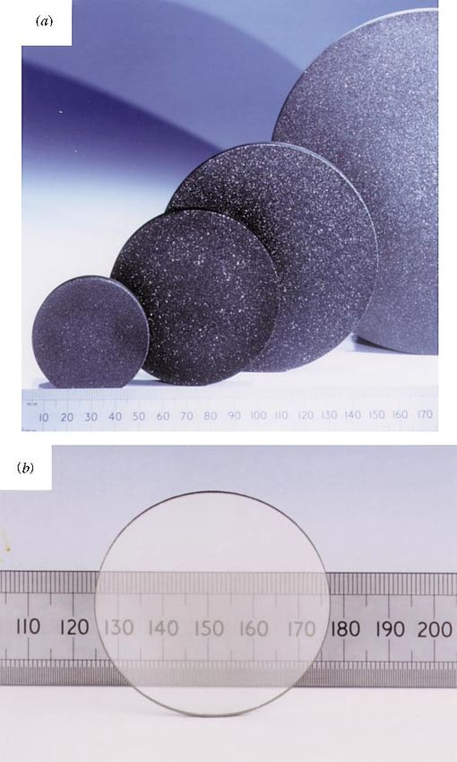
Phil. Trans. R. Soc. Lond. A (2000)Diamond thin films 487 Figure 6. (a) 2–6 in (5–15 cm) diameter diamond wafers on Si, and (b) optically transparent free-standing diamond windows (reproduced with permission of Dr Christoph Wild, Fraunhofer Institut für Angewandte Festkörperphysik, Freiburg, Germany). carat (0.2 g) of CVD diamond fell below $1 for the first time in the year 2000, and this will make the use of CVD diamond much more economically viable, and finally allow engineers the opportunity to exploit its vast array of outstanding properties in a wide variety of applications. Phil. Trans. R. Soc. Lond. A (2000)
488                                   P. W. May

   Cutting tools. The extreme hardness of diamond, coupled to its wear resistance,
makes it an ideal candidate for use in cutting tools for machining non-ferrous metals,
plastics, chip-board and composite materials. Indeed, HPHT industrial diamond has
been used for this purpose since the 1960s, and remains a lucrative commercial
process today. This involves either gluing the diamond grit to a suitable tool (saw
blades, lathe tools, drill bits), or consolidating the diamond grit with a suitable binder
phase (e.g. Co or SiC) to make a hard, tough and durable composite. CVD diamond
is beginning to be used in a similar way, by coating the diamond directly onto the
surface of the tungsten carbide tool-pieces. Initial tests (Reineck et al. 1996; Karner et
al. 1996) indicate that such CVD diamond-coated tools have a longer life, cut faster,
and provide a better finish than conventional WC tools. The term non-ferrous should
be emphasized here, since this highlights one disadvantage that diamond has over
other tool materials: it reacts with iron, and so cannot be used to cut ferrous materials
such as steel. However, some of the newer composite metals that are beginning to
be used in the aerospace and automobile industries, such as Al/Si, are excellent
candidates for diamond-coated cutting tools, as they are very difficult to machine
with conventional materials.
  Thermal management. Modern high-power electronic and opto-electronic devices
suffer severe cooling problems due to the production of large amounts of heat in a
small area. In order to cool these devices, it is essential to spread the narrow heat
flux by placing a layer of high thermal conductivity between the device and the
cooling system (such as a radiator, fan, or heat sink). CVD diamond has a thermal
conductivity that is far superior to copper over a wide temperature range plus it has
the advantage of being an electrical insulator. Now that large-area CVD diamond
plates with thermal conductivities ca. 20 W cm−1 K−1 are available (Wörner et al.
1996), this material is beginning to be used for a variety of thermal management
applications. These include submounts for integrated circuits (Boudreaux 1995), heat
spreaders for high-power laser diodes (Troy 1992), or even as a substrate material
for multi-chip modules (Lu 1993). The result of this application in device fabrication
should be higher speed operation, since devices can be packed more tightly without
overheating. Reliability can also be expected to improve, since for a given device,
junction temperatures will be lower when mounted on diamond.
  Optics. Because of its optical properties, diamond is beginning to find uses in
optical components, particularly as a free-standing plate for use as an infrared (IR)
window in harsh environments. Conventional IR materials, especially in the 8–12 µm
wavelength range (such as ZnS, ZnSe and Ge), suffer the disadvantage of being brittle
and easily damaged. Diamond, with its high transparency, durability and resistance
to thermal shock, is an ideal material for such applications. An example (Dischler &
Wild 1998) of an optical quality diamond window can be seen in figure 6b.
   Electronic devices. The possibility of doping diamond and so changing it from an
electrical insulator to a semiconductor opens up a whole range of potential electronic
applications. However, there are a number of major problems which still need to be
overcome if diamond-based devices are to be achieved. First, CVD diamond films are
polycrystalline containing many grain boundaries, twins, stacking faults and other
defects, which all reduce the lifetime and mobilities of carriers. For effective device
operation, single-crystal diamond films are required, and this has been the driving
force behind the development of the BEN techniques for producing textured films,

Phil. Trans. R. Soc. Lond. A (2000)
Diamond thin films                                     489

                           36 µm

    Figure 7. Selective area deposition of a patterned diamond film on Si (reproduced with
              permission of Professor John Wilson, Heriot-Watt University, UK).

mentioned earlier. Another problem, which to some extent has recently been solved,
is the requirement that the diamond films must be patterned to produce features of
similar size to those used in microcircuitry, typically a few micrometres. Fortunately,
diamond can be etched in O2 -based plasmas, provided a suitable non-erodible mask
is used. Alternatively, a technique known as selective area deposition (SAD) (Chalker
& Johnston 1996) can be employed, whereby the diamond is encouraged to grow on
only certain parts of the substrate. Whichever technique is used, diamond films can
now be patterned to geometries suitable for all but the most demanding devices
(see figure 7). The final, and probably the most difficult problem to solve in order
to be able to create diamond devices, is that of doping the diamond reliably and
reproducibly. p-type doping is relatively straightforward, since addition of a few
ppm of a boron-containing gas such as B2 H6 to the CVD process gas mixture is all
that is required to incorporate B into the lattice. However, the close packing and
rigidity of the diamond lattice make doping with atoms larger than C very difficult.
This means that dopants which are routinely used to n-dope Si, such as P or As,
cannot easily be used for diamond. The development of a successful n-doping process
has taken a considerable time, and only very recently have a few reports appeared

Phil. Trans. R. Soc. Lond. A (2000)
490 P. W. May from a group in NIRIM claiming success in this area (Koizumi et al. 1998; Sakaguchi et al. 1999). Despite these difficulties, diamond-based devices are gradually beginning to ap- pear, and may become the material of choice for electronic applications involving high power and/or high temperature. Indeed, diamond Schottky diodes have been demonstrated operating at up to 1000 ◦ C (Ebert et al. 1994). Transistor structures have also been attempted, with varying degrees of success. On the basis of the various field effect transistor devices that have been fabricated, an extremely high power handling density of 30 W mm−1 has been predicted. But despite these advances, diamond electronics is still in its infancy. A more detailed account of the various diamond device structures attempted to date can be found in Dischler & Wild (1998) and Spear & Dismukes (1994). SAW devices. One type of electronic device which can use impure, thin polycrys- talline CVD diamond (as opposed to single-crystal diamond), is the surface acoustic wave (SAW) filter. A SAW filter is a device which can transform radio frequency elec- tronic signals into mechanical vibrations, and vice versa (Morgan 1985). They are used in the communications industry, where high frequency radio waves need to be generated by electronic circuitry, and subsequently broadcast by a transmitter. These radio waves are then collected by a receiver and must be reconverted back to elec- tronic signals for further processing. The limiting factor in most current SAW devices is the maximum speed with which signals can propagate through the device from one set of circuitry to the other, and this depends largely upon the speed of sound (the acoustic wave) along the surface of the device material. For future high-performance devices, a SAW material is needed which can operate at 10 GHz or higher frequen- cies, and diamond is the obvious candidate. This is because the diamond lattice is so stiff that the speed of sound through it is extremely fast (17 500 m s−1 ). In practice, the diamond film is part of a multilayered structure, with a piezo-electric material such as ZnO, LiNbO3 or LiTaO3 deposited on top of the diamond to convert the mechanical vibrations of the diamond to electrical signals (Nakahata et al. 1996). Some companies (such as Sumitomo in Japan) are already exploiting diamond-based SAW filters in commercial mobile phone equipment, and it is likely that within a few years a diamond SAW filter will be an essential component of all high frequency communications equipment, including telephone networks, cable television and the Internet. Field emission displays. Another device which can use polycrystalline CVD dia- mond, and which is causing a great deal of interest at the moment, is the idea of using diamond as an electron emitter in flat-panel displays. The electronic properties of diamond are such that when it is biased negatively in vacuum, electrons are ejected from its surface. This process is also common in most metals, except that in metals the electrons have to overcome an energy barrier, or work function, to escape from the surface. In diamond this barrier has been measured and found to be very small, maybe even negative, and this has given rise to the term ‘negative electron affinity’ (Himpsel et al. 1979). In practice, this means that devices based on the electron emission properties of diamond could consume very low power levels and hence be extremely efficient. The electrons emitted from the surface are accelerated using a positively biased grid to strike a phosphor screen, causing light to be emitted. Each emitting diamond crystal, or group of crystals, would form a ‘pixel’ on a flat-panel Phil. Trans. R. Soc. Lond. A (2000)
Diamond thin films                            491

                                                          25 kV 100 µm

           Figure 8. A diamond-coated tungsten wire grown in an HFCVD reactor.

display screen. Unlike their major competitors (liquid crystal displays (LCDs)), dia-
mond cold cathode field emission displays (FEDs) would have high brightness, have
a large viewing angle, and be insensitive to temperature variations. Also, because of
their relative simplicity, it is possible that diamond FEDs could be scaled up to large
areas that would be impossible with LCDs, maybe even metres square!
   Electrochemical sensors. Doped CVD diamond films can be used for electrochemi-
cal applications, especially in harsh or corrosive environments. Conducting diamond
electrodes, made by boron-doping CVD diamond films, have been found to have a
very large potential window in water (Martin et al. 1995). This is a great advantage
over other electrode materials, such as Pt, which dissociate water at higher electrode
potentials resulting in the unwanted evolution of hydrogen and oxygen. For diamond-
based electrodes, this hydrogen evolution rate is much slower, allowing much higher
electrode potentials to be used. This permits the chemistry of redox couples to be
studied, which would otherwise be inaccessible (Bouamrane et al. 1996). Diamond
electrodes may find applications in analysis of contaminants, such as nitrates, in
water supplies, and even in the removal of those contaminants.
   Composite reinforcement. Diamond fibres and wires have been fabricated (May et
al. 1994) (see figure 8), which show exceptional stiffness for their weight. If growth
rates can be increased to economically viable levels, such diamond fibres may find
uses as reinforcing agents in metal matrix composites (Partridge et al. 1994), allowing
stronger, stiffer and lighter load-bearing structures to be manufactured for use in,
say, aerospace applications. Hollow diamond fibres and two-dimensional diamond
fibre mattings or weaves (Nicholson et al. 1996) have also been demonstrated, and
could form the basis of smart composite structures.
  Micromechanical devices and sensors. Diamond could also potentially be used in
micromachines (Hunn et al. 1994), since the ability to produce thin films which can
be precisely patterned, coupled to its stiffness and wear resistance makes it a good

Phil. Trans. R. Soc. Lond. A (2000)
492 P. W. May
candidate for hard wearing micromechanical structures, such as cogs and gears. This
technology is still in its infancy, but a few such structures, such as pressure and
temperature sensors have already been demonstrated (Werner et al. 1995).
Particle detectors. One area where CVD diamond is already beginning to find a
market is as a ‘solar-blind’ detector for ultraviolet (UV) light and high energy parti-
cles. High-performance UV detectors have been demonstrated (McKeag & Jackman
1998) and are now in commercial production. Diamond can be used to detect other
high energy particles, such as alpha- and beta-particles and neutrons), and be used
as a replacement for Si in the next generation of particle accelerators (Dischler &
Wild 1998; Mainwood et al. 1995). Since diamond has a similar response to dam-
age by X-rays and gamma-rays as human tissue, a possible application is in medical
applications, as a dosimeter for radiation exposure.
9. Summary
Despite the rapid progress made in the past 10 years in the science and technology
behind diamond film CVD, the commercialization of this amazing material is still
in its infancy. Researchers and industry are currently concentrating upon developing
methods to scale up the CVD processes and reduce production costs to the point at
which it becomes economically viable to use diamond as the material of choice. With
the 21st century upon us, we are still some way from diamond becoming the engineer’s
dream of being ‘the ultimate engineering material’. However, some devices are already
in the marketplace, such as diamond heat spreaders, windows, cutting tools, and
SAW filters. In the next few years we can expect to see diamond films appearing
in many more applications, especially in electronics. Perhaps the most likely ‘killer
applications’ which will firmly establish diamond as a 21st-century material will be
in the area of specialized flat-panel displays and high temperature electronics, for
which the total available market in the year 2000 has been estimated at $435 million
and $16 billion, respectively (Dischler & Wild 1998). In some ways this may be a
shame, since familiarity with diamond as just another commonplace material may
remove some of the glamour and mystique surrounding the world’s most sought-after
gemstone.
The author thanks the Royal Society for funding and the award of a University Research Fel-
lowship. He also thanks Professor John Wilson (Heriot Watt University) and Dr Christoph Wild
(Fraunhofer Institut für Angewandte Festkörperphysik, Freiburg, Germany) for giving permis-
sion to reproduce their figures and photographs.
References
Angus, J. C., Will, H. C. & Stanko, W. S. 1968 J. Appl. Phys. 39, 2915.
Asmann, M., Heberlein, J. & Pfender, E. 1999 Diamond Relat. Mater. 8, 1.
Bachmann, P. K., Drawl, W., Knight, D., Weimer, R. & Messier, R. 1988 In Diamond and
diamond-like materials. Mater. Res. Soc. Symp. Proc. EA-15, 99.
Bachmann, P. K., Hagemann, H.-J., Lade, H., Leers, D., Picht, F., Weichert, D. U. & Wilson,
H. 1994 Mater. Res. Soc. Symp. Proc. 339, 267.
Bouamrane, F., Tadjeddine, A., Butler, J. E., Tenne, R. & Levy-Clement, C. J. 1996 Electroanal.
Chem. 405, 95.
Phil. Trans. R. Soc. Lond. A (2000)Diamond thin films 493 Boudreaux, P. J. 1995 In Applications of Diamond Films and Related Materials: 3rd Int. Conf. (ed. A. Feldmann, Y. Tzeng, W. A. Yarbrough, M. Yoshikawa & M. Murakawa), p. 603. Washington, DC: NIST. Bundy, F. P. 1980 J. Geophys. Res. 85, 6930. Chalker, P. R. & Johnston, C. 1996 Physica Status Solidi 154, 455. Deryagin, B. V., Fedoseev, D. V., Lukyanovich, V. M., Spitsyn, B. V., Ryanov, A. V. & Lavren- tyev, A. V. 1968 J. Cryst. Growth 2, 380. Deryagin, B. V., Spitsyn, B. V., Builov, L. L., Klochov, A. A., Gorodetskii, A. E. & Smol’yanimov, A. V. 1976 Dokl. Akad. Nauk. SSSR 231, 333. Dischler, B. & Wild, C. (eds) 1998 Low-pressure synthetic diamond. Springer. Ebert, W., Vescan, A., Borst, T. H. & Kohn, E. 1994 IEEE Electron. Devices Lett. 15, 289. Eversole, W. G. 1958 US Patent nos 3030187, 3030188. Field, J. E. 1992 The properties of natural and synthetic diamond. Academic. Glumac, N. G. & Goodwin, D. G. 1993 Mater. Lett. 18, 119. Goodwin, D. G. & Butler, J. E. 1997 In Handbook of industrial diamonds and diamond films (ed. M. A. Prelas, G. Popovici & L. K. Bigelow), ch. 11. New York: Marcel Dekker. Hanssen, L. M., Carrington, W. A., Butler, J. E. & Snail, K. A. 1988 Mater. Lett. 7, 289. Himpsel, F. J., Knapp, J. A., van Vechten, J. A. & Eastman, D. E. 1979 Phys. Rev. B 20, 624. Hunn, J. D., Withrow, S. P., White, C. W., Clausing, R. E., Heatherly, L. & Christensen, C. P. 1994 Appl. Phys. Lett. 65, 3072. Jubber, M. G. & Milne, D. K. 1996 Physica Status Solidi 154, 185. Kamo, M., Sato, Y., Matsumoto, S. & Setaka, N. J. 1983 Cryst. Growth. 62, 642. Karner, J., Pedrazzinni, M., Reineck, I., Sjöstrand, M. E. & Bergmann, E. 1996 Mater. Sci. Eng. A 209, 405. Koizumi, S., Kamo, M., Sato, Y., Mita, S., Sawabe, A., Reznik, A., Uzan-Saguy, C. & Kalish, R. 1998 Diamond Relat. Mater. 7, 540. Lu, G. 1993 In Applications of Diamond Films and Related Materials: 2nd Int. Conf. (ed. M. Yoshikawa). Tokyo: MYU. McKeag, R. D. & Jackman, R. B. 1998 Diamond Relat. Mater. 7, 513. Mainwood, A. (and 11 others) 1995 J. Phys. D 28, 1279. Martin, H. B., Argoitia, A., Angus, J. C., Anderson, A. B. & Uziel, L. 1995 In Applica- tions of Diamond Films and Related Materials: 3rd Int. Conf. (ed. A. Feldmann, Y. Tzeng, W. A. Yarbrough, M. Yoshikawa & M. Murakawa), p. 91. Washington, DC: NIST. Matsumoto, S., Sato, Y., Kamo, M. & Setaka, N. 1982a Jpn. J. Appl. Phys. Part 2 21, 183. Matsumoto, S., Sato, Y., Tsutsumi, M. & Setaka, N. 1982b J. Mater. Sci. 17, 3106 May, P. W., Rego, C. A., Thomas, R. M., Ashfold, M. N. R., Rosser, K. N. & Everitt, N. M. 1994 Diamond Relat. Mater. 3, 810. Mollart, T. P. & Lewis, K. L. 1999 Diamond Relat. Mater. 8, 236. Morgan, D. P. 1985 Surface wave devices for signal processing. Elsevier. Morrison Jr, P. W. & Glass, J. T. 1994 In Properties and growth of diamond (ed. G. Davies), p. 380. London: INSPEC. Nakahata, H., Kitabayashi, H., Fujii, S., Higaki, K., Tanabe, K., Seki, Y. & Shikata, S. 1996 IEEE Ultrasonics Symp., San Antonio, p. 285. Nicholson, E. D., Meaden, G., Kalaugher, E., Partridge, P. G., Ashfold, M. N. R., May, P. W. & Wisbey, A. 1996 Diamond Films Technol. 6, 217. Ohtake, N. & Yoshikawa, M. 1990 J. Electrochem. Soc. 137, 717. Partridge, P. G., May, P. W., Rego, C. A. & Ashfold, M. N. R. 1994 Mater. Sci. Technol. 10, 505. Poferl, D. J., Gardner, N. C. & Angus, J. C. 1973 J. Appl. Phys. 44, 1418. Phil. Trans. R. Soc. Lond. A (2000)
You can also read