Digital Radio Front-End strategies provide game-changing benefi ts for small cell base stations
←
→
Page content transcription
If your browser does not render page correctly, please read the page content below
W H I T E             PA P E R
                               Hardik Gandhi,
                  Radio IP Development Manager,
                        Debbie Greenstreet,
                     Strategic Marketing Director,
                                  Joe Quintal,
                    Senior Applications Engineer,
                               Texas Instruments     Digital Radio Front-End
                                                     strategies provide game-
                                                     changing benefits for
                                                     small cell base stations

Abstract                                             Introduction
It is no secret that small cell base stations        Explosive growth in cellular data usage is dictating communication infrastructure evolution,
are expected to be a major lifesaver in the          pushing for increased capacity and reduction in cost and environmental impact. Heteroge-
wireless data deluge by helping to provide           neous networks – coexisting macro/pico/femto cells, along with advanced receivers and
significant capacity gains as part of 3G and         transmitters to maximize spectral efficiency can provide the required boost in capacity. At the
4G wireless heterogeneous networks. While            same time, improving power efficiency will be a key consideration for next-generation radio
the industry standards and algorithms are            architectures.
mostly in place for these heterogeneous net-           As wireless service providers and base station manufacturers aggressively push towards
works to function, power, performance and            deployment of small cell base stations, they are faced with challenges to meet viable business
cost hurdles must be met before small cell           and network performance models: approximately a 10x reduction of power consumption,
base station solutions manifest into practi-         size and cost compared to the traditional macro base station. A lot of focus has been given
cal reality. Base station manufacturers tend         to single-chip base station SoCs, along with optimized small cell software as a key strategy
to focus their attention on the performance          for achieving these objectives, and rightfully so as the SoC architecture and software plays a
and attributes of the small cell baseband            significant factor in small cell cost, power, size and performance. The digital radio front ends
System on Chips (SoCs). The baseband SoC             of macro base stations are typically on separate boards, sometimes even in separate enclo-
silicon and software does contribute to a sig-       sures. Since the output power for small cells is significantly lower than for traditional macro
nificant portion of the small cell solution per-     base stations, one approach could be to scale down the macro design (perhaps also reducing
formance, however the digital radio front end        functionality) to achieve acceptable performance at reduced size and cost.
portion of the design can have a substantial           However, as we make the paradigm shift from a macro to a small cell base station, there
impact as well and is often overlooked. This         are additional opportunities for further integration of the digital radio front end technology
white paper focuses on the digital front end         and the baseband processing executed by the SoC, as well as portions of the radio front end
portion of the small cell base station and           with the analog RF circuitry. Newer interface standards offer more optimized board layout and
delves into design factors that play a sig-          interconnect options, offering additional optimization. Finally, by leveraging the radio front end
nificant role in achieving the performance           power amplifier linearization techniques, even further gains can be made in small cell solution
and power targets demanded by small cells.           power reductions without compromising performance.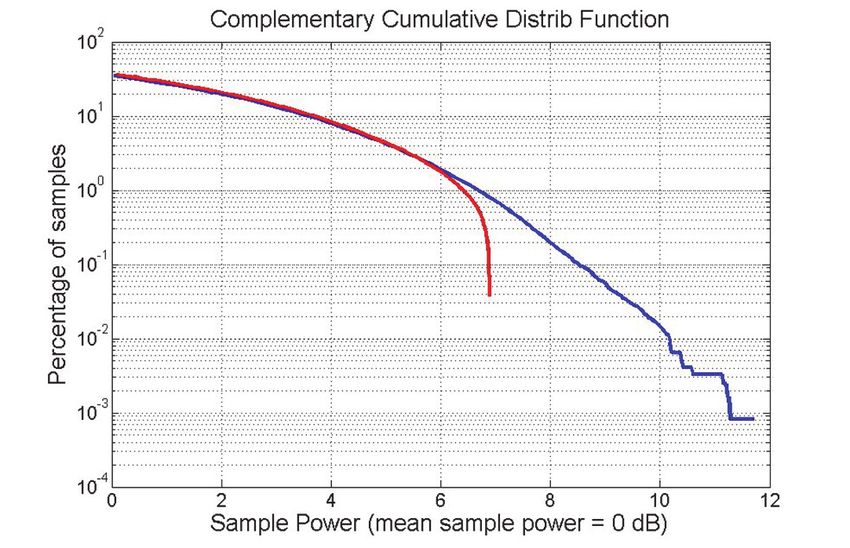
2    Texas Instruments

                   From macro cells             Traditional macro base station architectures can roughly be divided into three functional categories: control
                      to small cells            processing, baseband (BB) processing and radio front end. While some level of integration of these func-
                                                tions is happening today, the control, baseband and some of the radio front end functions of a macro base
                                                station are typically on a single board, with the bulk of the radio front end often times on a separate board,
                                                and maybe even in a separate enclosure, as depicted in Figure 1. Macro base-station radios often have
                                                dozens of integrated circuits partitioned along functional boundaries, with baseband and control processing
                                                in a leading-edge process node digital CMOS SoC, digital front end technologies in digital CMOS ASICs or
                                                ASSPs, data-converters in CMOS/BiCMOS technologies with 1–8 converters per device, and RF up and down
                                                conversion functions like I/Q modulators and mixers, buffers, attenuators, etc. in typically separate devices
                                                with optimal noise and linearity performance.

     Figure 1: Macro base-station radios often have dozens of integrated circuits partitioned along functional boundaries

                                                   When small cell base stations became an integral topic of heterogeneous network planning several years
                                                ago, the success strategy hinged on the assumption that they would be much smaller and lower power and
                                                hence, employ a single-board solution with much fewer numbers of discrete components compared to macro
                                                cells. Since then, as operators and the 3GPP organization continue to hone the small cell requirements and
                                                algorithms, the performance requirements and complexity has grown, providing further challenges in meeting
                                                those form factor and power expectations.
                                                   While macro cells typically range in output power from anywhere between 10W to 60W or more, the
                                                small cell umbrella covers a variety of applications with different output power ranges (transmit power at the
                                                antenna):

                                                   • Indoor femto cells: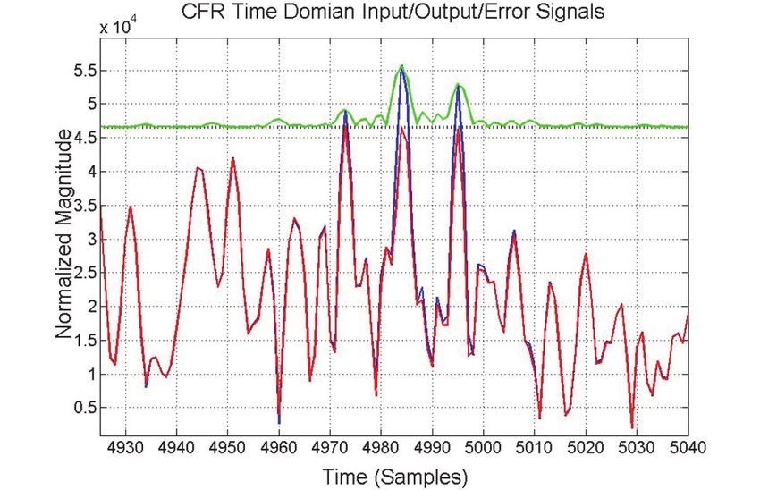
Texas Instruments 3

                                               • Outdoor pico cells: 1–2W Pout
                                               • Micro cells: 2–5W Pout and larger

                                              To meet area and cost targets in small cells, the stringent performance requirements imposed on analog/
                                            RF components are often relaxed, with the expectation that evolution of digital impairment correction
                                            algorithms would help recover any loss in performance. For example, in order to lower size, the transceiver
                                            front ends would use surface or bulk acoustic wave (SAW or BAW) duplexers, which are much smaller and
                                            cheaper than the ceramic/cavity duplexers normally used in macro cells. But they add significantly to post-PA
                                            RF power loss. Due to this the RF PAs for small cells often need to operate at 2–3dB higher Pout than what
                                            the antenna actually radiates, pushing them further into non-linear operating regions, in turn requiring linear-
                                            ization algorithms to ensure compliance with spectral emissions and modulation accuracy limits.
                                              The fact that a vast majority of, perhaps all, small cell base stations will be deployed with enclosures that
                                            have no special provisions for air cooling makes reducing every watt of power consumption (and resulting
                                            heat dissipation) ever so important. Along with the motivation to reduce power, cost and area, small cells
                                            also need to support newer features like network listening modes for spectral sniffing and synchronization,
                                            and be more frequency agile to be able to support different 3G/4G frequency bands and signal bandwidths
                                            with as few variants of the design as possible. These requirements drive a rethink of traditional architectures,
                                            potentially evolving into a configuration as depicted in Figure 2.

Figure 2: Small cell base station architectures strive for single-board solutions with minimal number of discrete components

                                              Next-generation small cell architectures can achieve these goals by taking advantage of advances in many
                                            areas:

                                               • Aggressive power optimization solutions
                                                     • PA linearization techniques like digital pre-distortion (DPD) in combination with crest factor reduc-
                                                        tion (CFR) techniques help lower overall system power consumption significantly, enabling more
                                                        PA choices – cheaper PAs and less expensive board and enclosure designs, which help minimize
                                                        BOM cost

Digital Radio Front-End strategies provide game-changing benefits for small cell base stations                                                     May 2013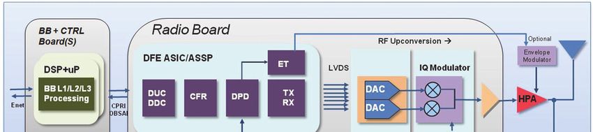
4    Texas Instruments

                                                  • PA Linearization techniques also provide margin for system performance – extending the reach
                                                      and performance of a small cell solution (bigger cell size, less interference) which maximizes
                                                      system efficiency
                                               • Flexible IF architectures and optimized interfaces
                                                  • For traditional high-performance macro base stations, a costly heterodyne design has until now
                                                      remained the de facto radio topology. A direct-conversion, or homodyne architecture, where the RF
                                                      signal is directly down-converted to a BB signal or vice versa without any intermediate frequency
                                                      stages has many attractive features. It is also referred to as a zero IF architecture. A zero-IF (or
                                                      very-low-IF) approach enables dramatically reducing component count and thus footprint and cost
                                                      of radio transceivers. Reducing the number of parts also simplifies the supply chain and manufac-
                                                      turing and improves yield. Zero-IF architectures provide a great deal of flexibility in frequency plan-
                                                      ning and allow multi-mode and/or multiband operations with minimal changes to baseband digital
                                                      and analog circuitry. Zero IF is not a new concept: radio designers have used these architectures
                                                      for low-end handsets and some base-station designs. Historically, many of the benefits offered by
                                                      a zero-IF architecture have been offset by a series of problems – I/Q distortion, DC offset and LO
                                                      leakage being some of the most critical. Until recently, these technical barriers in receiver design
                                                      have prohibited its practical implementation for high-performance base stations. But with advances
                                                      in digital SoCs, novel, adaptive digital compensation techniques can be implemented cost-effectively
                                                      to mitigate these problems, and allow radio designers to fully exploit all the advantages this archi-
                                                      tecture choice brings to the table.
                                                  • Newer interface standards, like JESD204B, help optimize board-level layout, reduce power
                                                      consumption and enable faster time to market compared to traditional parallel LVDS/LVCMOS
                                                      interfaces.
                                               • Higher levels of integration
                                                  • Aggressive integration of traditionally discrete digital-/analog-processing components into area,
                                                      cost and power-optimized System-on-Chips. As shown in Figure 2, all of the high throughput
                                                      digital processing could be combined in one optimized leading-edge digital process node BB SoC,
                                                      combining control, baseband and radio processing, including some or all elements of the digital
                                                      radio front end processing. All of the data conversion and RF up/down conversion processing
                                                      could be combined in another radio SoC in a process node suited for analog/RF performance, with
                                                      elements of the digital front end processing included to provide required analog/RF impairment
                                                      correction.

                                              Every watt of power saved with the above techniques translates into a proportional reduction in operational
                                            expenditure for the carrier (OPEX) as well as into proportional reduction in cooling (enclosure) costs, and may
                                            provide a wider choice in component selection and resulting reduction in capital expenditure (CAPEX). With

    Digital Radio Front-End strategies provide game-changing benefits for small cell base stations                                                 May 2013
Texas Instruments 5

                                       the sheer number of small cell deployments projected, even an 10W power saving per small cell base sta-
                                       tion (typical savings with CFR/DPD for a 0.5W 2×2 small cell) using advanced technologies can translate to
                                       significant savings in lifetime operating expenses (~$1M/year for a single dense metro with 70k small cells
                                       deployed), as well as reducing the environmental impact of vast scale deployment.
                                          Digitally assisted RF transceiver architectures utilizing the techniques described in this paper take us a
                                       step closer to an all-digital radio and help next-generation base-station transceivers meet some of the newer
                                       challenges as they emerge. These novel technologies enable the small cell architecture to take on a single-
                                       board solution as depicted in Figure 2, and are discussed in more detail in the rest of the paper.

             Digital Front End         The air interface for cellular base-station radios requires essential digital, analog and RF signal-processing
        technologies overview          components to prepare the modulated samples for transmission, or extract modulated data from received
                                       signals at the antenna, and is functionally partitioned as depicted in Figure 3.

                                                Backhaul     Layer 3                                                                  Radio
                                                                          Layer 2     Layer 1       DFE        Analog     Antenna
                                                            Transport
                                                Interface                                                                             Interface

                                                               Packets           Frames           Samples            RF Carriers

                                       Figure 3: Functional partitioning of cellular base station processing components

                                          Beyond providing an interface (LVDS/LVCMOS or JESD204A/B SerDes) to analog-to-digital and digital-
                                       to-analog data converters, the digital front end blocks perform a variety of critical functions which can be
                                       roughly classified into two categories:

                                           1. Channelization and re-sampling functions – these are mandatory signal-processing functions to
                                              be performed for any type of base station [micro or macro, Time Division Duplex (TDD) or Frequency
                                              Division Duplex (FDD), 3G or 4G]
                                              • Carrier filtering to comply with spectral emission masks and spectral leakage requirements, includ-
                                                 ing root-raised-cosine filtering (RRC) and/or linear channel equalization.
                                              • Tuning and channel aggregation/distribution – essential for multi-carrier and/or multi-standard
                                                 base stations.
                                              • Gain, phase, delay adjustments and power-measurement functions

                                          Figure 4 on the following page shows a flexible digital up/down converter block (DUC/DDC) that performs
                                       these mandatory channelization and resampling functions. Programmable finite impulse response (FIR) filters,

Digital Radio Front-End strategies provide game-changing benefits for small cell base stations                                                May 2013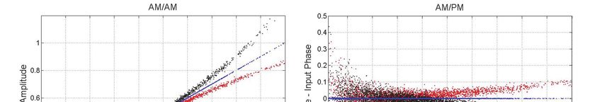
6    Texas Instruments

                                                    SmallͲcells
                                                    Æ to/from
                                                    L1/L2                                                                                      To CFR
                                                    processing                                                                                 or
                                                    MacroͲcells                                                                                 From
                                                    Æ to/from                                                                                  RX
                                                    CPRI/OBSAI

                                                                      Symbolrate                                              Upsampled
                                                                      BaseͲband                                               composite
                                                                      I/QData                                                Antenna
                                                                                                                               streams

                                            Figure 4: Block diagram of an implementation of essential channelization and re-sampling functions

                                            farrow-based resampling filters, cascaded-integrator-comb (CIC) filters and numerically controlled oscillators
                                            (NCOs) and mixers are the essential signal processing blocks that perform these functions.

                                               2. Power amplifier (PA) linearization and RF impairment correction functions – these are
                                                   optional in the true sense, but often mandated by system efficiency and cost requirements. Every
                                                   Analog/RF component suffers from some impairment (group delay, non-linear distortion, gain/phase
                                                   imbalance) at its optimal operating point (best efficiency, best dynamic range, best noise figure) that
                                                   can be corrected by digital pre- or post-processing. Some of the key algorithms for impairment cor-
                                                   rection include:
                                                   • Crest Factor Reduction – required to limit signal peak to average power ratios to reduce PA
                                                       peak power and linearity requirements and hence system cost
                                                   • Digital Pre-Distortion – required to improve system linearity to allow PAs to be operated more
                                                       efficiently, reducing both system cost (CAPEX) and operating expenses (OPEX)
                                                   • I/Q distortion and DC offset/LO-leakage correction – essential to enable zero-IF system
                                                       architectures, which in turn help reduce system cost and improve flexibility.

                         Crest Factor       Fourth-generation multi-carrier communication systems based on orthogonal frequency division multiplex-
                           Reduction        ing (OFDM) as well as third-generation code-division multiple-access (CDMA) based systems exhibit signals
                                            with high peak-to-average ratios (PARs), also known as crest factors. The non-constant envelope-modulation
                                            techniques employed in such systems have stringent Error Vector Magnitude (EVM) requirements. This re-
                                            quires a highly linear PA amplitude and phase response, often resulting in an increased PA back-off (driving
                                            the PAs at lower output power levels) to maintain acceptable linearity to meet spectral mask and modulation
                                            accuracy requirements. PAs are most power efficient at close to peak drive levels. A high PA back-off results
                                            in a drastic reduction in PA efficiency.

    Digital Radio Front-End strategies provide game-changing benefits for small cell base stations                                               May 2013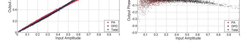
Texas Instruments 7

                                             Crest-factor-reduction techniques strive to reduce the peak-to-average power ratios of transmit signals by
                                          deliberately introducing noise into the signals within the EVM and Adjacent Channel Power Ratio (ACPR) limits
                                          imposed by the standards. Multi-carrier (and even single-carrier LTE) signals can have a peak-to-average
                                          power ratio (PAR) as high as 12dB. The application of CFR can reduce signal peaks by as much as 4–6dB,
                                          with acceptable in-band EVM degradation, allowing the PA to operate at higher input/output power levels
                                          (resulting in more efficiency) while maintaining linearity at the output of the PA.
                                             Even for the smallest category of small cells with 100–200mW antenna output power, the 4–6dB decrease
                                          in PA peak power through the use of CFR enables a roughly 2–4× difference in PA size and power efficiency,
                                          and a corresponding reduction in cost. This should be a key trade-off when doing power budgeting to meet
                                          small cell power over Ethernet (PoE) limits.
                                             Figure 5 shows CFR processing for a typical multi-carrier 3G test model signal. The Complementary Cumu-
                                          lative Distribution Function (CCDF) plot on the right shows the signal sample distribution before and after CFR.
                                          As can be seen, the signal peak-to-average power ratio is reduced from over 11dB to under 7dB. CFR can
                                          reduce the PAR even more, but would be limited by the EVM limits set for the standard. The plot on the left
                                          shows a snippet of the time domain waveform around a signal peak. A cancellation pulse scaled to the ap-
                                          propriate gain and phase is applied to the signal to reduce the peak amplitude to below a set threshold. The
                                          cancellation pulse needs to have an appropriate spectral shape suited to limit most of the noise in-band so as
                                          not to violate spectral mask requirements.

                                                       Cancelled
                                                       Peaks

         CFR Threshold                           CFR Input (blue)
                                                 CFR Output (red)
                                                 Cancellation (green)
                                                                                                              CFR Output            CFR Input

Figure 5: Crest-factor-reduction performance example

                                             CFR is usually applied in baseband at low sample rates suitable for digital signal processing. But the PAs
                                          operate on signals up-converted to RF frequencies. This up-conversion process will generate signal peaks
                                          that may not be visible at low baseband sample rates. For optimal peak cancellation, CFR signal processing

Digital Radio Front-End strategies provide game-changing benefits for small cell base stations                                                May 2013
8    Texas Instruments

                                           has to apply special interpolation techniques to estimate the RF signal peaks and apply fractionally adjusted
                                           cancellation pulses to the signal. Also special care needs to be taken to accommodate multiple overlapping
                                           peaks to limit over cancellation.

                             Digital       RF power amplifiers achieve maximum power efficiency near the saturation point of the PA (often listed as
                      Pre-Distortion       Psat or P1dB or P3dB in PA datasheets). Due to the inherent nature of LDMOS/GaN/GaAs power transistors,
                                           the PAs are most nonlinear near Psat (as shown in Figure 6 below), introducing severe distortion effects into
                                           the transmitted signals. As shown in Figure 7 on the following page, these effects manifest themselves as
                                           in-band distortion (degraded Error Vector Magnitude – EVM) and increased out-of-band spectral re-growth
                                           (degraded Adjacent Channel Leakage Ratio – ACLR). Minimum EVM and ACLR requirements are defined by
                                           regulatory bodies and OEMs need to add sufficient margin on top of these requirements to allow for perfor-
                                           mance variations with temperature and time (component aging). Very often the PA drive levels are backed off
                                           such that the signal falls within the linear region of the PA to avoid these distortion effects. But at these back-
                                           off regions, the PA power efficiency is extremely poor. Linearization techniques need to be employed to oper-
                                           ate the PA close to its saturation region, where it offers maximum output power and best power efficiency.
                                              A variety of power amplifier linearization techniques such as RF feed-forward, RF feedback, RF/IF pre-
                                           distortion and post-distortion have been proposed and implemented over the years. Of these, adaptive Digital
                                           Pre-Distortion (DPD) schemes have proven to be the most efficient and cost effective compared to traditional

                                                                   CFR reduces signal peaks to concentrate the signal power within a limited region –
                                                                                     allows pushing the PA output power higher

                                                                 DPD allows the PA to be operated closer to its saturation region to maximize efficiency -
                                                                        while still meeting Spectral Mask and Modulation Accuracy requirements

                                                                                                        Ideal (linear) PA
                                                                                                        response

                                                                                                                            Typical PA
                                                                      Optimal PA power efficiency                           response
                                                                      close to the saturation points        P3dB
                                                                      (P1dB/P3dB)                       P1dB
                                                  Output Power

                                                                                                               PA transistor characteristics cause
                                                                                                               signal distortion in and beyond this
                                                                                                               region because the output power drops
                                                                                                               below the ideal (linear) curve

                                                                                           Without CFR/DPD, the PA must be operated in this
                                                                                           region to avoid distortion

                                                                                                  Input Power
                                           Figure 6: Typical RF power amplifier response

    Digital Radio Front-End strategies provide game-changing benefits for small cell base stations                                                           May 2013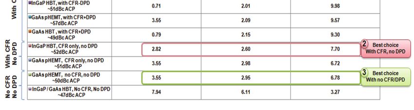
Texas Instruments 9

                                                               Non-Linear distortion causes out of band spectral
                                                               leakage (ACPR degradation)

                                                                            Non-Linear and linear distortion causes in-band
                                                                            error (EVM degradation)

                                       Figure 7: Effects of RF PA non-linearities

                                       analog/RF linearization techniques. Efficiencies of traditional LDMOS Class AB power amplifiers widely in use
                                       today when operated under a back-off condition range from 3–10%. However, with crest factor reduction
                                       and adaptive digital pre-distortion techniques, the efficiencies can be improved by 3 to 5 times. Newer PA
                                       topologies such as advanced Doherty, or Class AB with drain modulation, in combination with digital pre-
                                       distortion and newer GaN or GaAs power transistors, can achieve efficiencies over 50%.
                                          For small cell power amplifiers, DPD allows the PA to operate linearly closer to Psat, improving system ef-
                                       ficiency. DPD also enables more PA choices – cheaper PAs and less expensive board design minimizes BOM
                                       cost, and provides margin for system performance – extending the reach and performance of a small cell
                                       base station (bigger cell size, less interference). As discussed later in this whitepaper, DPD can provide from
                                       ~1W/antenna to ~20W/antenna system power savings for small cells ranging from 100mW to 2W antenna
                                       output power with exponential increase in savings beyond that.
                                          The idea behind Digital Pre-Distortion (DPD) is to cascade a non-linear system prior to the PA, which
                                       provides an inverse response to the PA such that the cascaded system has a linear response. As shown in
                                       Figure 8 on the following page, f(.) is the inverse of g(.) such that y is a linear representation of x (with the
                                       desired amplification factor). RF power amplifiers have complex non-linear models, made more complicated
                                       by the presence of memory effects. Memory effects refer to the bandwidth-dependant nonlinear behavior
                                       often exhibited by RF PAs. These encompass envelope memory effects and frequency response memory
                                       effects. Envelope memory effects are primarily a result of thermal hysteresis and electrical properties inherent
                                       to PAs. Frequency memory effects are due to the variations in the frequency spacing of the transmitted signal
                                       and are characterized by shorter time constants. These memory effects and non-linearity in general changes
                                       over time and temperature and requires a real time adaptive DPD correction.
                                          The plots in Figure 9 on page 11 show amplitude and phase responses of a typical RF PA, where with DPD
                                       the resulting outputs (in blue) are clearly much more linear compared to the original PA outputs (in red). Typi-
                                       cally, the harder a PA is driven to maximize its efficiency, the more severe the non-linear distortion and the

Digital Radio Front-End strategies provide game-changing benefits for small cell base stations                                                   May 2013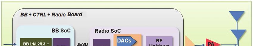
10 Texas Instruments

                                                                          DPD models a
                                                                          response inverse to                 Typical PA response
                                                                          the PA response

                                                                  Input Signal               Pre-Distorted               PA Output
                                                                                                Signal                    Signal

                                                                 DPD cancels out PA non-linearity and helps eliminate the distortion
                                                                 effects (ACPR and EVM degradation) from the PA output signal.

                                          Figure 8: A model for PA linearization via digital pre-distortion

                                           wider the bandwidth a PA has to support, the more severe the memory effects are, making the need for DPD
                                           even more pressing.
                                             The DPD non-linearity order, memory depth and adaptation rates are often PA and signal dependent, and
                                           a commercially viable small cell DPD solution has to envision all usage scenarios and draw reasonable trade-
                                           offs between performance and hardware and software computational requirements.

                      DC offset and        Direct conversion or zero-IF radio architectures are a popular choice for small cell transceiver design since
                      I/Q distortion       they use fewer components and are easier to integrate comparing with the conventional heterodyne archi-
                     compensation
                                           tectures. But those benefits also come with several well-known impairments, namely I/Q imbalance and DC
                                           offset.
                                             In a direct conversion transceiver, a quadrature modulator (QM) implements I/Q modulation and RF upcon-
                                           version, while a quadrature demodulator (QDM) realizes I/Q demodulation and RF downconversion. Because
                                           of the limitation in analog circuit precision, the quadrature carriers used in QM and QDM cannot have exactly
                                           the same amplitude and a perfect 90-degree phase difference that are essential for accurate signal conver-
                                           sion. Similarly, the analog reconstruction filters on the I and Q paths may not match exactly. These imperfec-
                                           tions are called I/Q imbalance, which causes cross talk between I and Q channels and creates undesired
                                           images of the original signal. In addition, because of limited isolation in analog components, some of the local
                                           oscillator (LO) power leaks into the RF output, which creates LO spikes in transmitted signal and DC offset in

   Digital Radio Front-End strategies provide game-changing benefits for small cell base stations                                               May 2013
Texas Instruments 11
Figure 9: Power amplifier memory effects
received signal. For traditional high IF heterodyne architectures these unwanted images can be filtered out by
analog/RF filters. But for zero-IF architectures these unwanted distortion images fall very close to or right on
top of the signal bands of interest, degrading signal SNR/EVM and/or violate spectral emissions limits, and
are very expensive (or often impossible) to eliminate via analog filtering. Digital pre- and post-compensation
techniques have to be employed to compensate for these distortions. Further complicating matters, these
distortion components are often frequency-dependent and may vary over time as components age, requiring
adaptive cancellation techniques.
Most existing compensation techniques treat transmit and receive I/Q imbalances separately. To compen-
sate for I/Q imbalance in the transmitter, the receive side is either assumed to have dedicated feedback loops
or digital demodulators with perfect quadrature carriers. To compensate for I/Q imbalance in the receiver,
the transmit side is usually assumed to be free of I/Q imbalance. For optimal zero-IF transceivers, the above
limitations are often impractical, resulting in the transmitter and receiver distortion components coexisting
and overlapping with each other, making extraction of the respective distortion compensation coefficients
ever more complicated.
JESD204 The push for ever more compact small cell enclosures to minimize visual impact and installation costs
necessitates highly condensed transceiver board layouts. Traditional data-converter interfaces based on
parallel LVDS or LVCMOS signaling protocols require considerable board area and a great deal of analysis
and special layouts to minimize skew across data bits and optimize the setup/hold times relative to the clock
traces. Board bring up with high-speed parallel interfaces is a big challenge and often gates system/software
bring-up and delays time to market.
JESD204 is a new standard that defines a serial communications link between data converters (ADCs
and DACs) and other devices such as FPGAs, DSPs, ASICs and clocking devices. Similar to other more
well-known signaling protocols like PCIe or CPRI, this SerDes-based interface highly simplifies the digital
Digital Radio Front-End strategies provide game-changing benefits for small cell base stations May 201312 Texas Instruments
data interface between devices. With the clock embedded in the data stream and embedded algorithms to
optimize sampling of the data bits, this simplifies the routing between devices because there are much fewer
lanes on the PCB, and it simplifies system design and board bring-up – no setup/hold time margin across as
many as 16 LVDS pairs with one data clock to worry about.
This new standard reduces the number of I/Os and thus pin count of devices allowing for smaller pack-
ages, and offers a flexible and scalable solution to accommodate different data traffic needs (e.g., multiple
ADCs on one JESD differential pair).
JESD204A (ratified in 2008) and JESD204B (ratified in 2011) both provide support for multiple lanes
per converter or multiple converters per lane. JESD204B supports data rates up to 12.5 Gbps compared to
3.125 Gbps for JESD204A. In addition, the JESD204B Subclass 1 operating mode provides support for ac-
curate synchronization across multiple converters. Multiple transmitters and receivers can get synchronized
in order to obtain a deterministic latency across multiple devices. This requires the use of an external system
reference signal (also known as SysRef) for synchronization. SysRef signals and device clocks need to be
distributed with matched length to all devices in order for the internal “local multi frame clocks (LMFC)” to
be synchronized properly. This ensures that the SysRef signal gets processed at the same instant across all
devices. But the JESD204B traces don’t have to be length matched. This provides a great deal of flexibility
in board layouts while still maintaining synchronization and deterministic latency across devices. The spatial
benefits can be clearly seen in Figure 10.
Dual 14bit Data Dual 14bit Data
converter converter
• DDR LVDS • JESD204B
• 16 diff pairs • 4 diff pairs @ 3.1Gbit
(14 data + clock + sync) or
• 2 diff pairs @ 6.2Gbit
Figure 10: Comparison of sample layouts with traditional LVDS and newer JESD interfaces
Shrinking cost of Current macro cell system architectures often employ discrete DFE solutions with built-in linearization func-
linearization tions (see reference 1 for an example). With macro cells typically designed for 10W–60W or higher antenna
output power, the 1–2W per antenna linearization cost is a small fraction of the overall system power budget
and is dwarfed by the power savings linearization brings to the table.
For small cell applications, with these discrete linearization solutions, the break-even PA output power at
which linearization starts adding net benefit is high. But with high levels of integration and digital technology
Digital Radio Front-End strategies provide game-changing benefits for small cell base stations May 2013Texas Instruments 13
scaling, benefit of linearization may be seen even for the lowest class of small cell applications. Many techno-
logical advances contribute to the shrinking cost of linearization, some of them being:
• High levels of integration in finer lithography SoCs:
As advanced DFE technologies were evolving over the last decade or so, low investment cost (but
high power and high production cost) ASIC/ASSP or FPGA solutions were effective given the pace
of change. But as DFE technologies have become more mature, and with built in flexibility in newer
DFE architectures, integration with other high-throughput baseband and control-processing functions
in deep sub-micron process nodes becomes more attractive, and allows for significant reduction in
power and cost for the same functionality compared to discrete solutions. As an example and shown in
Figure 11, over 4× reduction in power and 7× reduction in cost (die area) can be seen as we progress
from stand-alone DFE solutions in 90nm to integrated DFE solutions in 28nm.
Technology Scaling
100 90nm
80
60
Area
65nm
40
40nm
20 28nm
0
0 20 40 60 80 100
Power
Figure 11: Reduction in power and area with semiconductor technology scaling
• More power and area efficient interfaces between devices:
Higher amounts of integration, and new high-speed serial interfaces can help with substantial reduc-
tion in board area and cost, eliminating what would have been seen as barriers to implementing
advanced high-sample-rate and adaptive algorithms. As we saw earlier, with JESD204B a 4 to 8×
reduction in the number of interface signals can be seen compared to traditional LVDS interfaces.
• Exploiting synergies enabled due to integration:
Various resources can be time shared between linearization and other functions required for small cell
operation – like sharing the feedback path with network listening for clock synchronization or spectral
monitoring, or sharing a DSP processor for L1/L2 processing as well as DPD and I/Q offset compensa-
tion adaptation. This helps reduce the number of components on the board significantly, and makes
optimal use of all available resources.14 Texas Instruments
The theoretical analysis shown in the graph in Figure 12 is based on the following assumptions:
• 2× increase in PA efficiency with CFR (typical 3dB PAR reduction and a linear PA efficiency curve)
• 3× increase in PA efficiency with DPD
• 4× drop in Linearization power from discrete to integrated DFE.
From this simplistic analysis it is apparent that with integrated DFE, benefits of linearization can be seen
even with output power as low as 150mW (region highlighted in the first gray circle), whereas with discrete
DFE, the break even power at which linearization adds value is around 0.5W (region highlighted in second
gray circle).
As seen from the graph in Figure 12, even at 150mW output power, greater than 2W power saving per
transmitter can be realized by including integrated CFR and DPD in the solution – Especially important
when trying to meet PoE (power over Ethernet) requirements.
16.0
Total Power Consumption - PA + Linearization (W)
14.0
12.0
10.0
8.0
6.0
4.0
2.0
0.0
0.10 0.20 0.30 0.40 0.50 0.60 0.70 0.80 0.90 1.00 1.10 1.20 1.30 1.40 1.50 1.60
Output Power (W)
Power Consumption Power Consumption Power Consumption Power Consumption
without CFR/DPD (W) with CFR, no DPD (W) with discrete CFR & DPD (W) with integrated CFR & DPD (W)
Figure 12: Theoretical analysis of linearization benefits
Lowering the bar To validate the benefits of linearization for the lowest class of small cells, a variety of small cell power ampli-
fiers from different vendors were evaluated in the lab with and without linearization, and the results are
encapsulated in Figure 13 on the following page. A 4-carrier W-CDMA test model signal was used for this
analysis. The PAs were tuned to output 200mW of transmit power, which after accounting for the 2–3dB post
PA loss due to filters/duplexers would correspond to a 100–125mW power level at the antenna. Per antenna
cost of integrated linearization (CFR/DPD datapath power, additional analog/RF power for requisite feedback
and differences in sampling/interface rates and power consumed in executing the adaptation algorithms) was
computed using 28-nm benchmarks and factored into the above analysis.
PA biasing and/or drain voltage can be tweaked to trade-off efficiency and linearity. For the above
experiments, without linearization, the PAs were biased to optimal linearity to meet spectral mask (ACPR)
Digital Radio Front-End strategies provide game-changing benefits for small cell base stations May 2013Texas Instruments 15
requirements. With linearization, the PAs were biased to optimal efficiency, and the linearization algorithms
provided required ACPR improvement to meet spectral mask requirements.
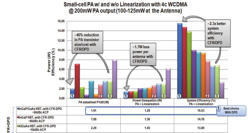
As can be summarized from the results in Figure 13, even for this low end of small cell applications, with
CFR/DPD one can select a PA with > 3× better PA efficiency (>27% compared to16 Texas Instruments
2W @ PA /
1W @ Antenna
With CFR/DPD:
~34% System
30.0 Efficiency
~19W power
savings/antenna
25.0
1W @ PA /
0.5W @ Antenna
With CFR/DPD:
20.0 ~21% System
PA+Linearization (W)
Power Consumption
Efficiency
~7.5W power Power Consumption
15.0
savings/antenna with CFR only, no DPD
(Average 8% PA Efficiency)
200mW @ PA / (W)
100mW @ Antenna Power Consumption
10.0 With CFR/DPD: with CFR/DPD
~16% System (Including PA+Linearization power)
Efficiency (W)
~1.3W power
5.0 savings/antenna
0.0
0.10 0.50 1.00
Antenna Output Power (W)
(Assuming 3dB post-PA loss)
Figure 14: Experimental analysis of DPD benefits – Exponential power savings at higher output powers
that its inclusion in any small cell solution is obviously warranted. If comparing results with neither CFR nor
DPD, against results with CFR and DPD, the projected power saving will be significantly higher. CFR and
DPD are both key to optimal linearization – one without the other may give you less than half the benefits,
especially at higher output power levels.
It’s also worth mentioning that PA non-linear behavior and memory effects become worse as signal
bandwidth increases, leading to decreasing ACPR. Most PA datasheets provide performance results using
single-carrier W-CDMA test model (5MHz) or LTE (10MHz) data. But small cell deployment scenarios call for
a wide range of signal bandwidths to be supported, up to 40MHz occupied and beyond, sometimes with non-
contiguous carrier placements like in LTE rel10 and 11 with inter- or intra-band carrier aggregation, which
increases the edge-to-edge signal spread to be supported. The expanding signal bandwidth requirements
make the need for state-of-the-art linearization performance even more pressing, which may not be seem
obvious from reading PA datasheets.
State-of-the-art DFE Integrated digital front-end radio technology blocks are key additions to next-generation TI SoCs based on the
capabilities integrated KeyStone II architectures, like the optimized dual-mode, dual-band small cell solution (TCI6630K2L) shown in
in next-generation
Figure 15 on the following page. Some of the key elements are briefly described below.
TI KeyStone II SoCs
• DDUC – Multiple digital up/down converter modules (shown as DDUCs in Figure 15) provide support
for a variety of signal types (W-CDMA, LTE-5MHz, LTE-10MHz, LTE-20MHz, etc.) with single- or multi-
band frequency configurations, with flexibility that allows re-configuring the BTS from single-mode
3G/4G to mixed-mode 3G/4G and vice versa. Also supported is both inter- and intra-band carrier
Digital Radio Front-End strategies provide game-changing benefits for small cell base stations May 2013Texas Instruments 17
MulticoreNavigator 28 nm
* + * +18 Texas Instruments
variety of least-squares type algorithms (Conjugate Gradient, Kalman, etc.) which can be implemented
in software on the high-performance floating-point DSP or ARM® cores, with additional hardware ac-
celeration options available for faster iteration times.
Figure 17 shows the PA output spectrum without DPD (red) and after DPD correction has been applied
(blue) for a representative small cell PA biased to optimal efficiency. As can be seen from this figure, TI’s
high-performance DPD enables the PA output spectrum to meet spectral mask requirements while achieving
highest obtainable power efficiency for a given PA.
Adjacent Channel
ACLR limit: Pre-DPD PA Output Spectrum –
-45dBc Violates Spectral Mask
Alternate Channel
ACLR limit: Post-DPD PA Output Spectrum -
-50dBc Meets Spectral Mask
With Margin
Figure 17: Example TI DPD performance results for a small cell PA
• TXRX – Novel joint I/Q distortion and DC offset/LO-leakage correction techniques like the one showed
in Figure 18 below and implemented in the TI TXRX modules (and accompanying integrated analog/
RF transceiver solution – AFE750x) can be used to jointly separate the transmit and receive side I/Q
Figure 18: A joint TX/RX I/Q distortion cancellation technique
Digital Radio Front-End strategies provide game-changing benefits for small cell base stations May 2013Texas Instruments 19
imbalance by introducing phase rotations in the analog domain. Since the phase rotations have differ-
ent effects on transmit and receive side I/Q imbalance, it enables using advanced digital algorithms to
separate the distortion effects and be able to pre-compensate (on the transmitter) or post-compensate
(on the receiver). Using real-time adaptive blind- or calibration-based least squares algorithms with
frequency dependent or frequency-independent compensation, optimal signal SNR and emissions-
mask compliance can be achieved. Figure 19 shows example results using such an algorithm, where
the I/Q distortion and DC offset images that would have violated spectral emissions requirements (or
degraded signal SNR if falling in-band underneath an adjacent carrier) are effectively eliminated down
to the system noise floor.
Figure 19: Example I/Q distortion and DC offset cancellation results
In addition to the above, TI’s digital radio modules include other functions like front-end and back-end
Automatic Gain Control loops (AGCs) that help maximize data-converter efficiency and reduce dynamic range
required in baseband processing, transmit/receive equalizers to compensate for analog/RF filter droop and
phase distortion effects and digital protection functions to limit signal excursions to prevent damage to the
PA and associated circuitry. These are welcome additions to any BTS transceiver design, providing significant
performance boost and RF/analog component cost reduction at the expense of low-cost integrated digital
logic.
State-of-the-art TI discrete and integrated data-converter, RF, clocking devices and BB SoCs now support
JESD204B subclasses 0 and 1 interfaces for optimal board designs, and enabling rapid system bring-up.
Last, but not least, integrated and tested, production-ready platform software from TI supporting not just
the baseband processing, but the digital radio processing, such as DDC/DUC, CFR and DPD libraries, as well
as analog/RF control enables rapid integration of system components and quick ramp to production.
As shown in Figure 20 on the following page, TI’s baseband SoC (TCI6630K2L) with integrated digital
front-end technologies, closely coupled with TI’s integrated radio transceiver solution (AFE750x) and other
clocking, power and RF devices from TI, with production ready software, enables a high-performance small
Digital Radio Front-End strategies provide game-changing benefits for small cell base stations May 201320 Texas Instruments
AFE750x
TCI6630K2L 2x2 TX and RX
PoE AVS 2x
2x TX Dig DAC 2x TX RF
2x 4x
DDUC / CFR / DPD/TXRX
2x
A15 C66x 2x RX Dig ET
ADC 2x RX RF
JESD204B TRX
Acceleration Pacs
GigE Auxiliary Receiver
GigE Network
PHY CoProcessor RX Dig ADC RX RF
Switch
Combiner
PCIe
PTP, Sync Duplexer
AFE750x HPA
USIM I2C USB 2x2 TX and RX LNA
JESD204B 2x
2x TX Dig DAC 2x TX RF
UART SPI DDR3 EMIF 2x
2x RX Dig ET
ADC 2x RX RF
TRX
PMU
Auxiliary Receiver
GPS DAC
WIFI DDR3 Flash RX Dig ADC RX RF
Clocking
Figure 20: TI’s small cell system solution
cell solution with optimized power consumption meeting PoE requirements, with a low BOM cost, fast time to
market, and flexibility to support evolving Het-Net strategies.
Conclusion • Integrated DFE solutions bring the benefits of linearization to lower output power systems; the use of
CFR/DPD for PA output as low as 200mW (100–125mW at the antenna) seems not only viable, but
mandatory to meet stringent PoE requirements.
• >3.4W total system power savings with CFR+DPD (compared to a solution with no CFR, no DPD)
for a 2×2 indoor small cell with a 25.5W overall system power budget seems very compelling.
• Power savings increase exponentially with higher output powers. Taking into account higher post-PA
losses of 2–3dB for small cells, savings can be much more.
• >15W saved with DPD (compared to a solution with CFR but no DPD) for a 2×2 system at 1W
output power per PA (0.5–0.625W output power at the antenna)
• >38W saved with DPD (compared to a solution with CFR but no DPD) for a 2×2 system at 2W
output power per PA (1–1.25W output power at the antenna)
• Dynamic nature of LTE signals, coupled with multi-mode and multiband requirements and the need
to extract the last ounce of system power savings make the need for best-in-class CFR and DPD
algorithms in integrated base-stations ever more compelling.
Digital Radio Front-End strategies provide game-changing benefits for small cell base stations May 2013Texas Instruments 21
• Flexibility of any linearization solution is key towards reuse across multiple classes of base stations,
and to tackle future advances in PA technology – Could there be in the near future a PA available that
can simultaneously transmit multiple signal bands spread over 100s of MHz of spectrum with accept-
able efficiency and cost? If so, a linearization solution which is capable of supporting such a PA is vital.
• TI’s flexible small cell SoCs with best-in-class integrated-linearization solutions enable
optimum system cost and power consumption across different classes of small cells, and
provide an easy upgrade path to satisfy future evolutionary needs.
References 1. H. Gandhi, W. Abbott “A digital signal processing solution for PA linearization and RF impairment cor-
rection for multi-standard wireless transceiver systems,” in Proc. IEEE European Microwave Confer-
ence. Sept. 2010.
Important Notice: The products and services of Texas Instruments Incorporated and its subsidiaries described herein are sold subject to TI’s standard terms and
conditions of sale. Customers are advised to obtain the most current and complete information about TI products and services before placing orders. TI assumes no
liability for applications assistance, customer’s applications or product designs, software performance, or infringement of patents. The publication of information
regarding any other company’s products or services does not constitute TI’s approval, warranty or endorsement thereof.
© 2013 Texas Instruments Incorporated SPRY236IMPORTANT NOTICE
Texas Instruments Incorporated and its subsidiaries (TI) reserve the right to make corrections, enhancements, improvements and other
changes to its semiconductor products and services per JESD46, latest issue, and to discontinue any product or service per JESD48, latest
issue. Buyers should obtain the latest relevant information before placing orders and should verify that such information is current and
complete. All semiconductor products (also referred to herein as “components”) are sold subject to TI’s terms and conditions of sale
supplied at the time of order acknowledgment.
TI warrants performance of its components to the specifications applicable at the time of sale, in accordance with the warranty in TI’s terms
and conditions of sale of semiconductor products. Testing and other quality control techniques are used to the extent TI deems necessary
to support this warranty. Except where mandated by applicable law, testing of all parameters of each component is not necessarily
performed.
TI assumes no liability for applications assistance or the design of Buyers’ products. Buyers are responsible for their products and
applications using TI components. To minimize the risks associated with Buyers’ products and applications, Buyers should provide
adequate design and operating safeguards.
TI does not warrant or represent that any license, either express or implied, is granted under any patent right, copyright, mask work right, or
other intellectual property right relating to any combination, machine, or process in which TI components or services are used. Information
published by TI regarding third-party products or services does not constitute a license to use such products or services or a warranty or
endorsement thereof. Use of such information may require a license from a third party under the patents or other intellectual property of the
third party, or a license from TI under the patents or other intellectual property of TI.
Reproduction of significant portions of TI information in TI data books or data sheets is permissible only if reproduction is without alteration
and is accompanied by all associated warranties, conditions, limitations, and notices. TI is not responsible or liable for such altered
documentation. Information of third parties may be subject to additional restrictions.
Resale of TI components or services with statements different from or beyond the parameters stated by TI for that component or service
voids all express and any implied warranties for the associated TI component or service and is an unfair and deceptive business practice.
TI is not responsible or liable for any such statements.
Buyer acknowledges and agrees that it is solely responsible for compliance with all legal, regulatory and safety-related requirements
concerning its products, and any use of TI components in its applications, notwithstanding any applications-related information or support
that may be provided by TI. Buyer represents and agrees that it has all the necessary expertise to create and implement safeguards which
anticipate dangerous consequences of failures, monitor failures and their consequences, lessen the likelihood of failures that might cause
harm and take appropriate remedial actions. Buyer will fully indemnify TI and its representatives against any damages arising out of the use
of any TI components in safety-critical applications.
In some cases, TI components may be promoted specifically to facilitate safety-related applications. With such components, TI’s goal is to
help enable customers to design and create their own end-product solutions that meet applicable functional safety standards and
requirements. Nonetheless, such components are subject to these terms.
No TI components are authorized for use in FDA Class III (or similar life-critical medical equipment) unless authorized officers of the parties
have executed a special agreement specifically governing such use.
Only those TI components which TI has specifically designated as military grade or “enhanced plastic” are designed and intended for use in
military/aerospace applications or environments. Buyer acknowledges and agrees that any military or aerospace use of TI components
which have not been so designated is solely at the Buyer's risk, and that Buyer is solely responsible for compliance with all legal and
regulatory requirements in connection with such use.
TI has specifically designated certain components as meeting ISO/TS16949 requirements, mainly for automotive use. In any case of use of
non-designated products, TI will not be responsible for any failure to meet ISO/TS16949.
Products Applications
Audio www.ti.com/audio Automotive and Transportation www.ti.com/automotive
Amplifiers amplifier.ti.com Communications and Telecom www.ti.com/communications
Data Converters dataconverter.ti.com Computers and Peripherals www.ti.com/computers
DLP® Products www.dlp.com Consumer Electronics www.ti.com/consumer-apps
DSP dsp.ti.com Energy and Lighting www.ti.com/energy
Clocks and Timers www.ti.com/clocks Industrial www.ti.com/industrial
Interface interface.ti.com Medical www.ti.com/medical
Logic logic.ti.com Security www.ti.com/security
Power Mgmt power.ti.com Space, Avionics and Defense www.ti.com/space-avionics-defense
Microcontrollers microcontroller.ti.com Video and Imaging www.ti.com/video
RFID www.ti-rfid.com
OMAP Applications Processors www.ti.com/omap TI E2E Community e2e.ti.com
Wireless Connectivity www.ti.com/wirelessconnectivity
Mailing Address: Texas Instruments, Post Office Box 655303, Dallas, Texas 75265
Copyright © 2013, Texas Instruments IncorporatedYou can also read