ECEN620: Network Theory Broadband Circuit Design Fall 2021 - Lecture 5: Charge Pump Circuits
←
→
Page content transcription
If your browser does not render page correctly, please read the page content below
ECEN620: Network Theory
 Broadband Circuit Design
 Fall 2021

Lecture 5: Charge Pump Circuits

 Sam Palermo
 Analog & Mixed-Signal Center
 Texas A&M University
Announcements
• HW2 due Oct 7
 • Requires transistor-level design
 • For 90nm CMOS device models, see
 https://people.engr.tamu.edu/spalermo/ecen689/cadence_90nm_2021.pdf
 • Can use other technology models if they are a
 90nm or more advanced CMOS node

• Exam 1 Thursday Oct 14
 • One double-sided 8.5x11 notes page allowed
 • Bring your calculator
 • Covers through Lecture 6

 2

Agenda
• Charge pump circuits
 • Basic operation
 • Techniques to improve static and dynamic
 current source matching

 3
References
• Design of Integrated Circuits for Optical
 Communications, B. Razavi, McGraw-Hill,
 2003.
• First Time, Every Time – Practical Tips for
 Phase-Locked Loop Design, D. Fischette,
 IEEE Tutorial, 2009.
• PLL/charge-pump papers posted on the
 website

 4
Analog Charge-Pump PLL Circuits
• Phase Detector
 PFD
 D UP ICP

• Charge-Pump
 Q
 CLKIN R
 Vctrl
 VCO CLKOUT
 CLKFB R DN
 Q R C2

• Loop Filter
 D
 ICP
 C1

• VCO
 Divider

 1/N

• Divider

 5
Charge Pump • Converts PFD output ICP signals to charge UP Charging Vctrl DN Discharging R C2 • Charge is proportional ICP to PFD pulse widths C1 F(s) Un - Averaged Charge - Pump Gain I CP Amps I CP Amps Averaged Charge - Pump Gain 2 rad I Amps Total PFD & Charge - Pump Gain CP 2 rad This gain can vary if a different phase detector is used 6
Charge Pump Implementations

 Single-Ended Fully Differential

 Vo+

 [Perrott] [Li TCAS1 2008]

 7
Simple Charge Pump
 M2
 VBP
 M4
 ICP
 D UP UP
 Q
 CLKIN R
 iCP
 Vctrl
 CLKFB R
 Q
 R C2
 D
 DN M3
 ICP C
 1
 VBN
 M1

• Issues
 • Skew between UPB and DN control signals
 • Matching of UP/DN current sources
 • Clock feedthrough and charge injection from switches onto Vctrl
 • Charge sharing between current source drain nodes’ capacitance and Vctrl

 8
Simple Charge Pump Skew Compensation T-gate M2 VBP • Adding a transmission gate in the D UP UP M4 ICP DN signal path helps to equalize CLKIN R Q the delay with the UPB signal for iCP Vctrl better overlap between the UP CLKFB R and DN current sources R Q C2 D DN DN M3 ICP C VBN 1 • Poor matching of UPB and DN M1 edge rates 3/2 Inverter Path M2 FODN > FOUP VBP D UP FOUP M4 ICP • Utilizing a 3-inverter UP path Q CLKIN R iCP and a 2-inverter DN path with Vctrl a higher fanout provides good CLKFB R R C2 D Q DN M3 matching of both delay and FODN ICP C 1 edge rates VBN M1 9
Charge Pump Mismatch Ideal locked condition, Actual locked condition but CP mismatch w/ CP mismatch M2 Tos VBP UP UP M4 IUP DN DN UP ∆ IUP IUP iCP Vctrl 2 R IDN IDN ∆ DN C2 Trst Trst M3 2 IDN C iCP iCP 1 VBN M1 Vctrl Vctrl t t ∆ • PLL will lock with static phase error if there is a charge pump mismatch ∆ • Extra “ripple” on Vctrl ∆ 2 • Results in frequency domain spurs at the reference clock frequency ∆ 2 offset from the carrier ∆ 2 10
PLL Output Spectrum w/ Spurs Time Domain Frequency Domain Pspur modulation f at fref fosc-fref fosc fosc+fref • Control voltage ripple results in periodic modulation of clock frequency • Spurs appear at fref relative to the carrier frequency • In order to minimize this, it is not only important to match the DC value of IUP=IDN, but also address dynamic current mismatches • Charge sharing • Charge injection and clock feedthrough 11
Charge Pump Feedback Biasing VBP M2 M4 IUP UP iCP IREF Vctrl R C2 DN M3 IDN C1 VBN M1 • PMOS IUP current source is feedback biased to match NMOS IDN current at the Vctrl output level 12
Charge Sharing on Vctrl
 Switches Off Switches On

 M2
 M2 Initial
 VBP CP
 VBP CP
 VP VP
 VP

 Vctrl Vctrl
 Vctrl
 CLF
 CLF VN
 VN t
 VN
 VBN CN
 VBN CN M1
 M1

• When switches are off, the PMOS current source drain
 discharges to VDD and the NMOS current source drain
 discharges to GND
• When switches are on, charge sharing occurs between
 the loop filter capacitance and these current source drain
 nodes, causing a level-dependent disturbance on Vctrl 13
Charge Pump w/ Improved Matching

 • Parallel path keeps current
 sources always on

 • Amplifier keeps current source
 VDS voltages constant resulting
 in reduced transient current
 mismatch (charge sharing)

 [Young JSSC 1992]

 14
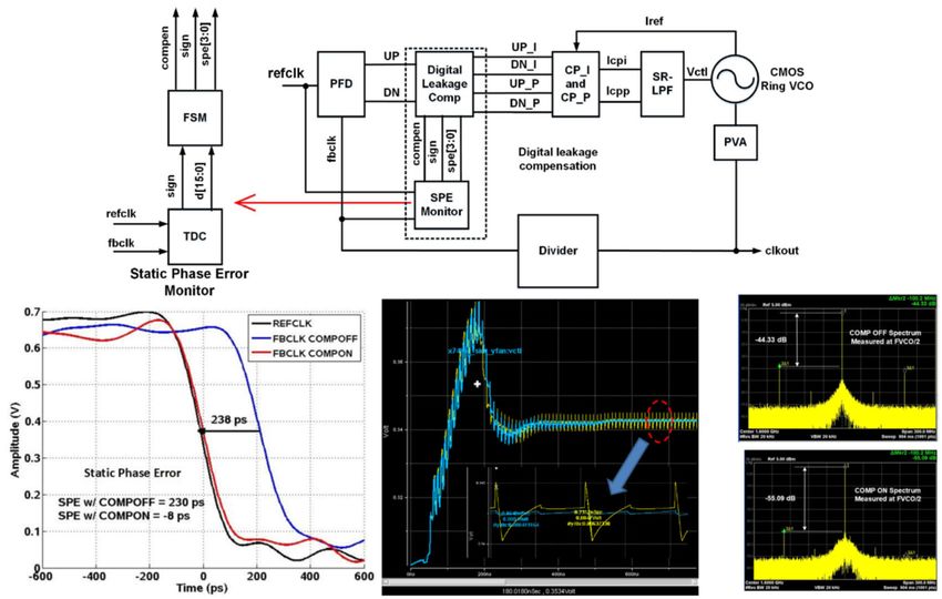
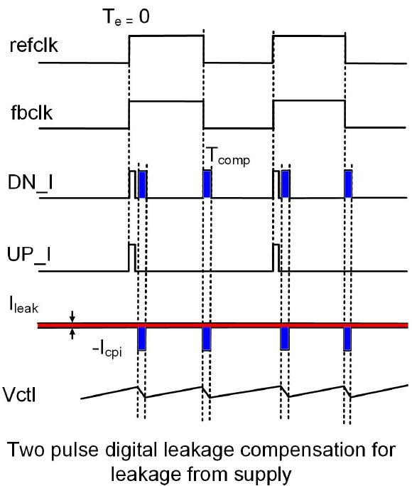
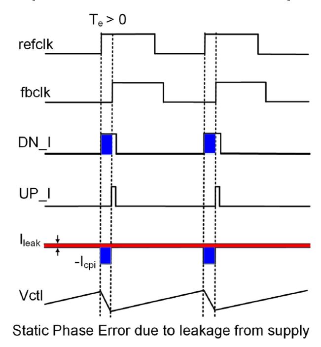
Digital Leakage Compensation
 [Fan ISSCC 2019]
• Charge pump off-state leakage causes PLL
 to lock with static phase error
• Compensated by additional digitally-controlled
 charge pump current pulses
• TDC detects phase error between input
 reference clock and feedback clock

 15
Charge Pump w/ Reversed Switches
• Swapping switches
 reduces charge injection
 • MOS caps (Md1-4) provide
 extra clock feedthrough
 cancellation
• Helper transistors Mx and
 My quickly turn-off current
 sources
• Dummy branch helps to
 match PFD loading
• Helps with charge
 [Ingino JSSC 2001]
 injection, but charge
 sharing is still an issue
 16
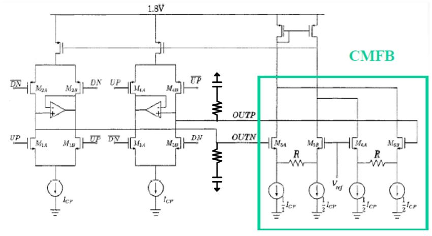
Fully-Differential Charge Pump

• CMFB loop adjusts the top current sources
 to match ICP at the differential loop filter
 common-mode level
 17
Everything But The Kitchen Sink
 [Cheng TCAS2 2006]

• This fully-differential charge pump uses many techniques to match the
 UP/DN current sources and mitigate charge injection and charge sharing
 • Dummy path M2 and M4 w/ feedback amps to match current source VDS
 • Dummy switches M1’ and M3’ provide charge injection cancellation
 • CMFB circuit matches UP/DN current at the filter common-mode output
 • Left and right-most feedback loop improve matching considering the
 differential loop filter control voltage
 • Additional PMOS current sources M11 & M12 extend matching over a wide
 voltage range
 18
Improved Matching w/ Differential Output
[Cheng TCAS2 2006]

 • The CMFB loop compensates for current source mismatch at the
 common-mode level
 • However, it cannot compensate for current source mismatch due to
 the differential control output voltage, as this voltage is symmetric
 with the common-mode
 • Additional feedback networks (OP1 & OP2) provide for improved
 matching with the differential control output voltage
 19
Additional Current Variation Suppression
[Cheng TCAS2 2006]

 • While matching is good at the control voltage extremes, the absolute
 current value falls due to finite current source output resistance
 • Additional PMOS current sources M1 and M2 provide additional NMOS
 current when the single-ended control voltage is low, which the main
 PMOS current source then tracks via feedback
 • This extends the voltage range over which the absolute charge pump
 current matches its nominal value
 20
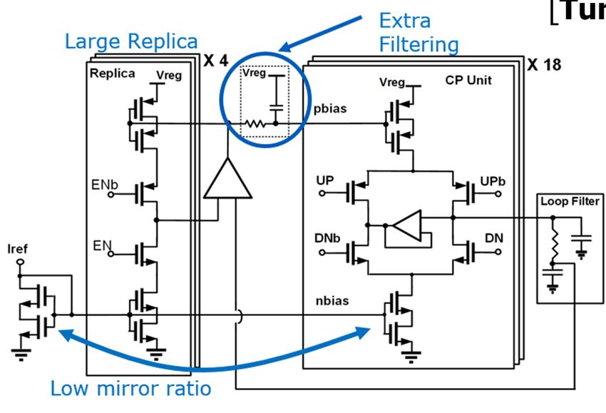
Low-Noise Charge Pump
 [Turker ISSCC 2018]

• Low mirroring ratio between input diode-connected
 transistor and charge pump current source
• Large replica bias transistors to set PMOS current
• Extra filtering in PMOS bias
• Stacked transistors utilized
 21
Next Time
• Loop Filter Circuits

 22
You can also read