Field-based Design of a Resonant Dielectric Antenna for Coherent Spin-Photon Interfaces
←
→
Page content transcription
If your browser does not render page correctly, please read the page content below
Field-based Design of a Resonant Dielectric
 Antenna for Coherent Spin-Photon Interfaces
 L INSEN L I 1 , H YEONGRAK C HOI 1 , M IKKEL H EUCK 1 , AND D IRK
 E NGLUND 1
 1 Research Laboratory of Electronics, Massachusetts Institute of Technology, Cambridge, MA 02139, USA
arXiv:2101.02366v1 [physics.optics] 7 Jan 2021

 * mheuck@mit.edu
 * englund@mit.edu

 Abstract: We propose a field-based design for dielectric antennas to interface diamond color
 centers with a Gaussian propagating far field. This antenna design enables an efficient spin-
 photon interface with a Purcell factor exceeding 400 and a 93% mode overlap to a 0.4 numerical
 aperture far-field Gaussian mode. The antenna design is robust to fabrication imperfections, such
 as variations in the dimensions of the dielectric perturbations and the emitter dipole location. The
 field-based dielectric antenna design provides an efficient free-space interface to closely packed
 arrays of quantum memories for multiplexed quantum repeaters, arrayed quantum sensors, and
 modular quantum computers.

 1. Introduction
 Color centers in diamond, such as the nitrogen-vacancy (NV) centers, are promising solid-state
 qubit systems due to their long spin coherence time and stable optical transition [1]. Moreover,
 recently studied group IV-vacancy centers in diamond such as silicon-vacancy (SiV) centers [2],
 germanium-vacancy (GeV) centers [3], and tin-vacancy (SnV) centers [4, 5] have resilient
 optical transitions [6]. Quantum applications such as quantum network [7], computing [8], and
 sensing [9], demand efficient coupling of quantum emitters to free-space propagating fields at
 cryogenic temperature. However, the free-space collection from the diamond color center is
 inefficient due to the large index mismatch between diamond and air. Recent photonic structures
 for improving free-space coupling include macroscopic solid immersion lenses produced by
 focused ion beam milling [10,11], recessed circular grating [12,13], metal plasmonic grating [14,
 15], metallic bow-tie antenna [16], nanopatch antenna [17], metasurfaces [18], and diamond
 nanopillars [19]. However, none of these designs combines a high Purcell effect and directional
 emission to jointly optimize spectral and spatial collection.
 Here, we introduce a design process for a dielectric antenna as a spin-photon interface to direct
 emission into the desired far-field mode. In particular, we introduce a transfer-matrix approach
 for 3D dielectric antenna design, combining gratings for directional mode coupling and cavity
 for Purcell enhancement. We apply this field-based design recipe to develop a diamond antenna
 that simultaneously achieves a Purcell factor of 420 and a 93% mode overlap with a 0.4 numerical
 aperture (NA) Gaussian beam, which has a 99% collection efficiency within an NA of 0.5. Thus,
 we estimate that the spin-photon interface efficiency can improve & 300 times compared with an
 NV dipole embedded in a 150 nm thick diamond membrane without nanostructures. Dielectric
 antennas, unlike metallic antennas [16], do not suffer from ohmic loss and quenching. The
 surface charge and spin noise are also alleviated by placing the closest etched surface more than
 one wavelength away from the dipole emitter [20]. We believe this quantum emitter antenna
 structure to be of great utility for quantum applications.
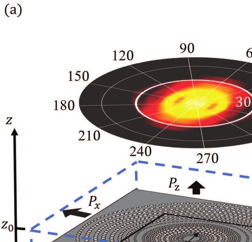
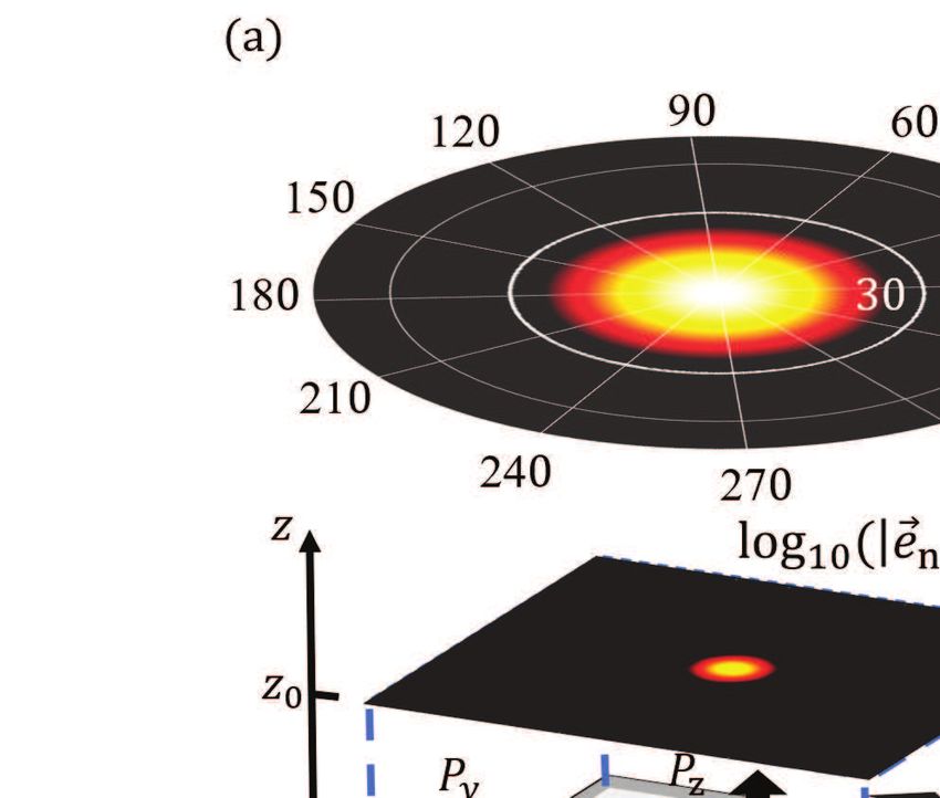
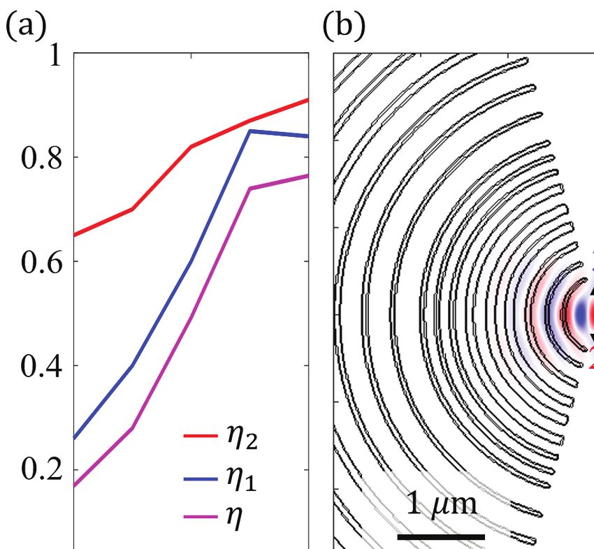
2. Antenna Design
As a figure of merit, we consider a coherent spin-photon interface efficiency = 1 2 , where 1
denotes the spin-antenna interface efficiency and 2 is the antenna efficiency. 1 is defined as
 0 ×
 1 = , (1)
 0 × + 1 − 0
where 0 denotes the radiation efficiency into the zero-phonon line (ZPL). The values of 0 for
NVs, SiVs, and SnVs are 3%, 7%, and 32%, respectively [6]. is the Purcell Factor, which
increases the spontaneous emission rate in the ZPL [21].
 The antenna far field ®far = ® + ® + ® is calculated on a hemispherical surface
located 0 = 1 m away from the center dipole source with finite-difference time-domain (FDTD)
simulations using Lumerical. We expect that to be zero because the electric far field
is perpendicular to the direction of propagation. Assuming a monochromatic antenna far
field with angular frequency and corresponding free-space wavelength , ®far ( 0 , , , ) =
 far exp[− ( − 2 )] ®far ( , ), where far is the electric
 0
 far-field amplitude. ®far ( , ) is the
 ∫ 2 ∫
dimensionless normalized far field. ®far ( , ) satisfies 0 0 | ®far ( , )| 2 sin d d = =
 /(2 +2 + ), where is the fraction of the emitted power propagating in the + direction.
 , , and are the radiated power propagating in the , , and direction, respectively (fig.
1(a)). The target far field ®tar ( 0 , , , ) has the same notation except the subscript.
 The antenna efficiency is the square of the mode overlap between ®far ( , ) and ®tar ( , ),
which we define as
 ∫ 2 ∫ 2
 ∗
 2 = ®far ( , ) · ®tar ( , ) sin d d . (2)
 0 0

We use a polarized Gaussian beam with NA = 0.4 as the target far field, ®tar ( , ) = 2.10 ×
exp(− tan2 /0.42 ) ®, which has 99% of its electromagnetic energy within an NA of 0.5 under
 ∫ 2 ∫
paraxial approximation. Here, ®tar ( , ) satisfies 0 0 | ®tar ( , )| 2 sin d d = 1. We also
consider the higher order correction for the polarized Gaussian beam [22], ®tar ( , ) = 2.14 ×
exp(− tan2 /0.42 ) [(1 − tan2 sin2 ) ® − tan2 sin cos ® − tan sin (1 − tan2 /2) ®]. It has
less than 1% variation in our final efficiency calculation.
 We summarize the field-based antenna design recipe as follows, providing the details of each
step in the supplementary material:
 Step 1: calculate the field profile of -oriented dipole, Re[ ( , , 0)]/max(| ( , , 0)|), in
the 150 nm thick unpatterned diamond membrane, as shown in fig. 1(a). We define the th phase
front as the points with phase difference from the dipole. The red arrows in fig. 1(a) indicate
the even number of the phase fronts, which will provide constructive interference when adding
dielectric perturbations to the diamond membrane. While the blue arrows indicate the odd
number of the phase fronts, which will provide destructive interference with the scattering of the
even number phase fronts when adding dielectric perturbations. We transform the target far field
 ®tar to the target near field ®ntar , which has azimuthal symmetry in amplitude. We add dielectric
perturbations along the phase fronts to make the mode normally incident on each perturbation
layer. Each curved perturbation layer is then approximated by a straight slot or periodic array of
holes. Under these approximations, the 3D design problem reduces to a 2D problem for slots
( - plane) or a 3D problem with a periodic boundary condition in the direction for the hole
array.
 Step 2: simulate an in-plane transverse-electric (TE) slab mode that is normally incident
on a single slot (width ) or a single period of the hole array (diameter , spacing ) with
FDTD simulation. The simulation yields a lookup table with reflection and transmission
coefficients as well as scattered near field distributions ® ( ) = ®near ( , 0 ) for slots or ® ( ) =
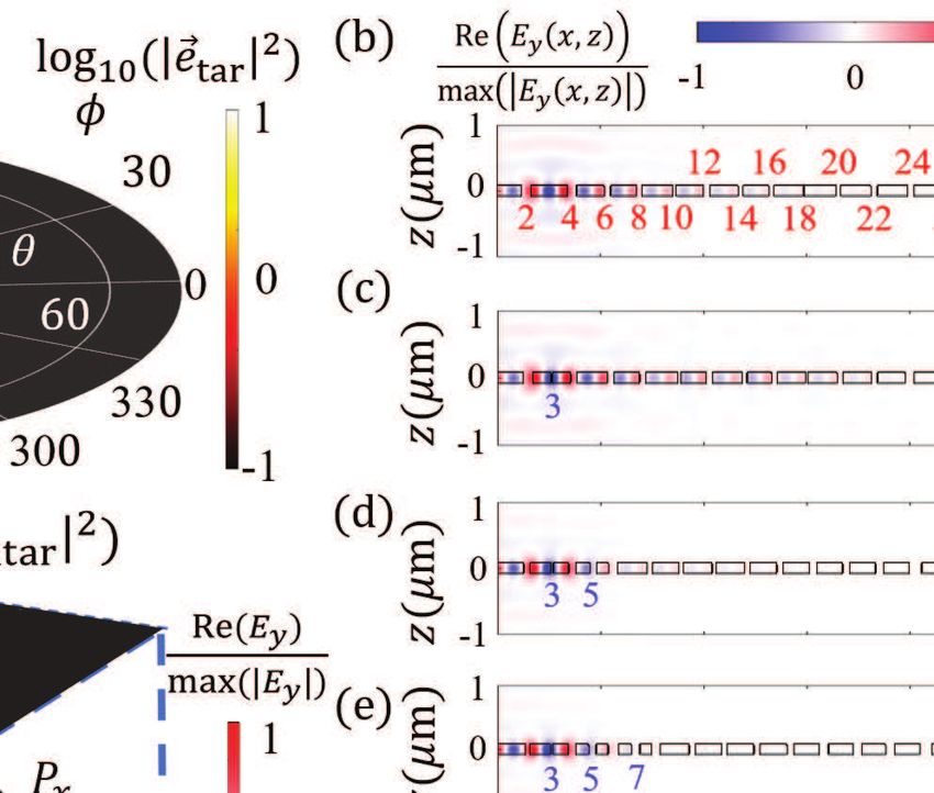
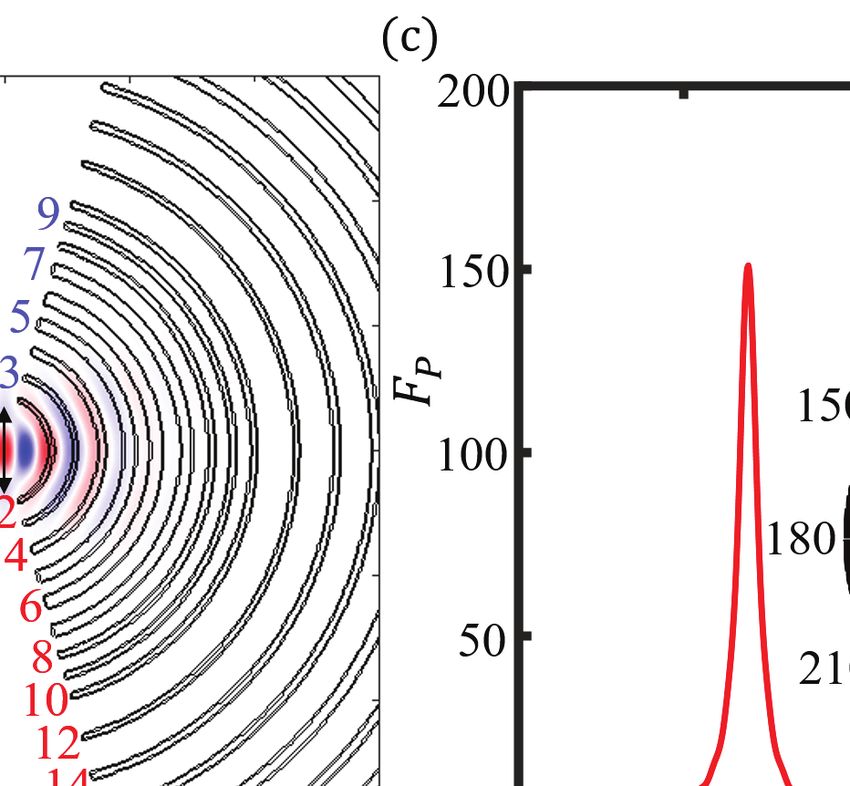
Fig. 1. Illustration of the field-based antenna design recipe. (a) 2D plots of the target far
 field log10 (| ®tar | 2 ) (top), the target near field log10 (| ®ntar | 2 ) (middle), and illustration
 of the unpatterned diamond slab with the dipole field overlaid with Re( )/max(| |)
 labeled with phase front number, assuming a perfect reflector at the = − min plane
 in the final structure. (b-e) Cross-sections of the diamond slab in the - plane [black
 rectangle plane in (a)] with the electric field Re( ( , ))/max(| ( , )|) overlaid.
 Slots are located at the even phase fronts (2, 4, ..., 26) in (b) for constructive interference.
 We add extra destructive interference slots around odd phase fronts in (c) (3), (d) (3
 and 5), and (e) (3, 5, and 7). The black line shows the slot edges. (f) Slot locations
 and widths for the antenna designs in (b-e).

 ®near ( , , 0 )d for hole array spacing . The th layer is at position with slot width
1
 ∫
 0
or hole parameters ( , ). Here, = 1, ..., max , where max is the maximum number of the
perturbation layers in the antenna.
 Step 3: apply transfer matrix model (TMM) to calculate the electric field at each layer [23,24].
Thus, we obtain the total scattered near field by coherently adding contributions from each
scattering layer using the lookup table. Here we use the slots located at even (2, 4, 6, ..., 26)
phase fronts of the dipole field in the unpatterned diamond slab as the initial guess structure.
 Step 4: calculate the mode overlap between the target and the antenna-scattered near field
along the line ( , = 0, = 0 ). The parameters ( , ) or ( , , ) of each layer are
optimized based on step 3 to maximize the mode overlap.
 Step 5: curve each slot or layer of holes to match the dipole emission phase fronts in the
diamond membrane (centered at = 0) and add a bottom reflector at = − min . We apply a
gradient descent optimization to maximize calculated from 3D FDTD simulations using the
result from step 4 as the initial guess structure.
 Step 6: add destructive interference slots (located at odd dipole field phase fronts like 3, 5,
and 7) in the initial guess structure in step 3 and redo step 4 and step 5 to increase the antenna
Purcell factor.
 Figure 1(b-e) plots the optimized antenna - cross-sections of step 4 overlaid with the electric
field Re( ( , ))/max(| ( , )|) without, with one, with two, and with three destructive
interference slots in the initial guess structure, respectively. Figure 1(f) details the values for
slot locations and widths in fig. 1(b-e).
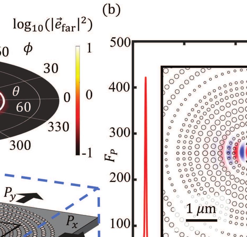
3. Simulation Results

 Fig. 2. (a) Efficiency vs. number of the destructive interference slots. (b)
 Re( )/max(| |) of the antenna with four destructive interference slots (at phase
 fronts 3, 5, 7, and 9). The black line shows the edge of the slot in the antenna structure.
 The red texts label phase front number of the constructive interference slots while the
 blue texts label the destructive interference slots. (c) Purcell factor spectrum and the
 far-field distribution log10 (| ®far | 2 ) of the antenna structure in (b).

 Figure 2(a) plots the efficiency as a function of the number of the destructive interference slots.
 increases with the number of destructive interference slots but saturates after four slots since
the field is confined in the central region as shown in fig. 2(b). Figure 2(b) shows the slot antenna
design with an efficiency = 75% for NVs using four destructive interference slots located at
phase fronts (3, 5, 7, and 9) (See supplementary material for detailed geometries). Figure 2(c)
plots the spectrum of the Purcell factor and far-field distribution of the antenna emission.
 Next, we use arrays of holes as the perturbation layer instead of the slots in our recipe. The
holes in the design have a minimum diameter (70 nm) than the minimum width of the slot (40
nm) relaxing fabrication difficulties. In addition, the design with holes ensures a connected
suspended structure even if the layers wrap around 360◦ with more degrees of freedom by hole
radii and spacing.
 Figure 3(a) shows the holey dielectric antenna structure along with the emitted far field. Figure
3(b) plots the spectrum of the Purcell factor and electric field distribution in the antenna’s -
cross-section. This structure simultaneously achieves a large mode overlap ( 2 reaches 87%)
and a large Purcell factor of 420, which makes the spin-photon interface reach 81% for NVs.
We optimized the structure for NV centers in diamond here. The design process can also work
for other emitters by changing the target resonant wavelength. In the supplementary material,
we also show an antenna design for the GaAs quantum dot system. In fig. 3(a), the distance
between the emitter and the closest dielectric perturbation is larger than / d (the resonant
wavelength in the material, where d is the refractive index of the diamond), which can alleviate
surface-charge noise. A previously reported bullseye antenna design has a collection efficiency
of 90% within NA = 0.65 and a Purcell factor of 20 in a GaAs quantum dot system [12]. Our
design applies the mode overlap between the antenna far field and the target Gaussian far field as
the figure of merit to have a better estimation in single-mode fiber collection efficiency, which
is important for quantum photonics, compared with the collection efficiency only considering
the electromagnetic energy within a certain NA. Our design can simultaneously achieve a large
mode overlap to a small NA mode and a large Purcell factor. The small NA collection can both
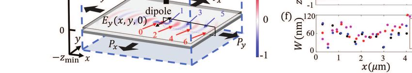
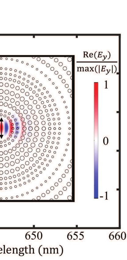
Fig. 3. (a) Illustration of the dielectric antenna structure, along with a plot of
 log10 (| ®far | 2 ) showing the far-field distribution. (b) Purcell factor spectrum of the
 antenna structure. The inset is a linear-scale plot of Re( )/max(| |) correspond-
 ing to the black square region in (a).

provide lower magnification for a larger field of view to examine more quantum emitters and
have a longer working distance between the objective lens and the cryogenic stage.

4. Sensitivity Analysis
The antenna design is tolerant to errors in dipole angle and location. Figure 4 plots the
efficiencies and Purcell factor as a function of the dipole’s misalignment in location (Δ , Δ , Δ )
and orientation, given by polar angle and azimuth angle . In fig. 3, the simulated dipole
orientation is in the direction corresponding to = 0◦ and = 0◦ . The normalized Purcell
Factor is 1 for the antenna structure shown in fig. 3. Figure 4(a) and 4(b) show how , 2 ,
and vary with the dipole orientation.
 Figure 4(c-e) summarize the effect of dipole displacements. The electric field changes rapidly
in the direction while changing gradually in the direction, as seen in fig. 3(b). Figure 4(c,d)
show that the Purcell factor decreases by 80% for Δ = 60 nm, but only 20% for Δ = 60 nm.
The Purcell factor drops 50% with Δ = 60 nm in fig. 4(e). For our antenna design for NVs,
the target implantation depth is 75 nm for the 150 nm diamond slab, which corresponds to a
60 keV implantation energy in Stopping and Range of Ions in Matter (SRIM) simulation [25].
From the simulation, we are 95% confidentp that the position variations of the implanted NV
centers are within |Δ | < 32 nm and (Δ 2 + Δ 2 ) < 28 nm under the Gaussian distribution
assumption [25]. In summary, though the dipole location variation changes the Purcell factor,
 2 is changed less than 2% when the angle variation is smaller than 45◦ since the dipole couples
to the antenna mode and the antenna mode couples to the free space target mode. follows the
expected overlap between the dipole ® and the mode’s electric field , ® i.e., ∝ ( | ® · ® ( ) | ) 2 ,
 | ® |· | ® |
where ® ( ) is the local electric field at the dipole emitter location , and | ® | is the maximum
value of the electric field in the antenna [26].
 We also investigate variations in the bottom reflector distance, hole sizes, and membrane
thickness (fig. 4(f-h)). We calculate , 2 , and at the resonant wavelength in the simulation.
The variation in the geometry will change the antenna resonant wavelength, but we can tune the
resonant wavelength to the target value using e.g. gas tuning [27]. The antenna performance
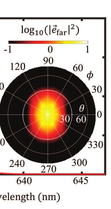
Fig. 4. The efficiencies and 2 , as well as the normalized Purcell factor =
 /max( ) as a function of changes in the dipole angle ( , ) (a, b), and dipole
 location (Δ , Δ , Δ ) (c-e), bottom reflector location (f), hole size (g), and membrane
 thickness (h), respectively. (i) Dependence of 1 on the Purcell factors for different
 types of quantum emitters. (j) Efficiency changes with and .

is robust to the bottom reflector distance as shown in fig. 4(f). From fig. 4(g) it is seen that
increasing the hole size by 10% only decreases the efficiency by 2%, whereas a reduction in hole
size by 10% reduces the efficiency by 12%. We observe a similar trend when decreasing rather
than increasing the membrane thickness, as seen in fig. 4(h). The antenna efficiency ( ) does
not decrease more than 12% for a ±10% geometry variation. The design with a large Purcell
factor (fig. 4(i)) maintains 1 even though the Purcell factor decreases by 70% due to variations
in dipole location, orientation, or nanostructure geometry. Within a ±10% geometry variation,
 2 does not decrease by more than 13% when the dipole is coupled to the antenna mode, which
leads to a robust spin-photon interface efficiency .
 Finally, we study the size dependence of the antenna. We reduce the antenna size to 2 × 2
where and are the length in the and direction. The simulation region is still
10 m × 10 m, where the diamond slab dimension is 10 m × 2 . The regions >
and < − are filled by air as the undercut trench [28]. In fig. 4(j), will not reduce more
than 5% when > 2 m fixing = 5 m. When reducing with the fixed = 5 m,
we notice that does not decrease more than 2% when > 1.2 m. The is over 73% with
dimension 4 m × 2.4 m for an NV center which resonant wavelength is = 637 nm.

5. Conclusion
In conclusion, we introduced a transfer-matrix approach for cavity-grating designs, enabling
efficient calculation of the cavity mode and the far field after an FDTD simulation of scattering
matrix primitives. We applied this method to design an efficient dielectric antenna for quantum
emitters. Specifically, the design achieves: (i) a relatively large emitter spacing to the first
etched surface of 1.4 / d to alleviate surface charge noise; (ii) 93% mode overlap with a
0.4 NA Gaussian beam which has 99% collection efficiency within an NA of 0.5, together
with a Purcell factor of 420; (iii) robustness to fabrication and dipole variations. While we
considered a diamond membrane here, the design applies to diverse materials such as Si or
GaAs. We anticipate that this design methodology and the resulting efficient quantum emitter
interfaces will benefit numerous applications, including multiplexed quantum repeaters [29],
arrayed quantum sensors [15, 30], boson sampling [31], and spin-based fault-tolerant quantum
computers [8].

Acknowledgments
The authors thank H. Raniwala and M. ElKabbash for useful comments. The authors acknowl-
edge the support from the Defense Advanced Research Projects Agency (DARPA) DRINQS
(HR001118S0024), the Air Force Office of Scientific Research MURI (FA9550-14-1-0052),
and the MITRE Quantum Moonshot Program. L. L. acknowledges support from the Analog De-
vices Fellowship, EFMA-1641064, QISE-NET NSF award DMR-1747426, and the NSF CIQM
program. H. C. acknowledges the Claude E. Shannon Fellowship and Samsung Scholarship.

References
1. M. W. Doherty, N. B. Manson, P. Delaney, F. Jelezko, J. Wrachtrup, and L. C. Hollenberg, “The nitrogen-vacancy
 colour centre in diamond,” Phys. Reports 528, 1–45 (2013).
2. M. Leifgen, T. Schröder, F. Gädeke, R. Riemann, V. Métillon, E. Neu, C. Hepp, C. Arend, C. Becher, K. Lau-
 ritsen et al., “Evaluation of nitrogen-and silicon-vacancy defect centres as single photon sources in quantum key
 distribution,” New journal physics 16, 023021 (2014).
3. T. Iwasaki, F. Ishibashi, Y. Miyamoto, Y. Doi, S. Kobayashi, T. Miyazaki, K. Tahara, K. D. Jahnke, L. J. Rogers,
 B. Naydenov et al., “Germanium-vacancy single color centers in diamond,” Sci. Reports 5, 12882 (2015).
4. T. Iwasaki, Y. Miyamoto, T. Taniguchi, P. Siyushev, M. H. Metsch, F. Jelezko, and M. Hatano, “Tin-vacancy
 quantum emitters in diamond,” Phys. Rev. Lett. 119, 253601 (2017).
5. M. E. Trusheim, B. Pingault, N. H. Wan, M. Gündoğan, L. De Santis, R. Debroux, D. Gangloff, C. Purser, K. C.
 Chen, M. Walsh et al., “Transform-limited photons from a coherent tin-vacancy spin in diamond,” Phys. Rev. Lett.
 124, 023602 (2020).
6. G. Thiering and A. Gali, “Ab initio Magneto-Optical spectrum of Group-IV vacancy color centers in diamond,”
 Phys. Rev. X 8, 021063 (2018).
7. P. C. Humphreys, N. Kalb, J. P. J. Morits, R. N. Schouten, R. F. L. Vermeulen, D. J. Twitchen, M. Markham, and
 R. Hanson, “Deterministic delivery of remote entanglement on a quantum network,” Nature 558, 268–273 (2018).
8. H. Choi, M. Pant, S. Guha, and D. Englund, “Percolation-based architecture for cluster state creation using photon-
 mediated entanglement between atomic memories,” npj Quantum Inf. 5, 1–7 (2019).
9. P. Cappellaro and A. Ajoy, “Stable three-axis nuclear spin gyroscope,” (2016). US Patent 9,417,068.
10. J. Hadden, J. Harrison, A. Stanley-Clarke, L. Marseglia, Y.-L. Ho, B. Patton, J. O’Brien, and J. Rarity, “Strongly
 enhanced photon collection from diamond defect centers under microfabricated integrated solid immersion lenses,”
 Appl. Phys. Lett. 97, 241901 (2010).
11. O. J. Trojak, C. Woodhead, S.-I. Park, J. D. Song, R. J. Young, and L. Sapienza, “Combined metallic nano-rings
 and solid-immersion lenses for bright emission from single inas/gaas quantum dots,” Appl. Phys. Lett. 112, 221102
 (2018).
12. J. Liu, R. Su, Y. Wei, B. Yao, S. F. C. da Silva, Y. Yu, J. Iles-Smith, K. Srinivasan, A. Rastelli, J. Li et al., “A solid-
 state source of strongly entangled photon pairs with high brightness and indistinguishability,” Nat. Nanotechnol. 14,
 586–593 (2019).
13. J. Zheng, A. C. Liapis, E. H. Chen, C. T. Black, and D. Englund, “Chirped circular dielectric gratings for near-unity
 collection efficiency from quantum emitters in bulk diamond,” Opt. Express 25, 32420–32435 (2017).
14. J. T. Choy, I. Bulu, B. J. Hausmann, E. Janitz, I.-C. Huang, and M. Lončar, “Spontaneous emission and collection
 efficiency enhancement of single emitters in diamond via plasmonic cavities and gratings,” Appl. Phys. Lett. 103,
 161101 (2013).
15. L. Kim, H. Choi, M. Trusheim, and D. Englund, “Absorption-based diamond spin microscopy on a plasmonic
 quantum metasurface,” arXiv preprint arXiv:2011.04885 (2020).
16. A. Karamlou, M. E. Trusheim, and D. Englund, “Metal-dielectric antennas for efficient photon collection from
 diamond color centers,” Opt. Express 26, 3341–3352 (2018).
17. S. I. Bogdanov, O. A. Makarova, X. Xu, Z. O. Martin, A. S. Lagutchev, M. Olinde, D. Shah, S. N. Chowdhury,
 A. R. Gabidullin, I. A. Ryzhikov et al., “Ultrafast quantum photonics enabled by coupling plasmonic nanocavities
 to strongly radiative antennas,” Optica 7, 463–469 (2020).
18. T.-Y. Huang, R. R. Grote, S. A. Mann, D. A. Hopper, A. L. Exarhos, G. G. Lopez, G. R. Kaighn, E. C. Garnett, and
 L. C. Bassett, “A monolithic immersion metalens for imaging solid-state quantum emitters,” Nat. communications
 10, 1–8 (2019).
19. T. M. Babinec, B. M. Hausmann, M. Khan, Y. Zhang, J. Maze, P. R. Hemmer, and M. Lončar, “A bright single
 photon source based on a diamond nanowire,” Nat. Nanotechnol. 5, 195 (2010).
20. H. Choi, D. Zhu, Y. Yoon, and D. Englund, “Cascaded cavities boost the indistinguishability of imperfect quantum
 emitters,” Phys. Rev. Lett. 122, 183602 (2019).
21. A. Faraon, P. E. Barclay, C. Santori, K.-M. C. Fu, and R. G. Beausoleil, “Resonant enhancement of the zero-phonon
 emission from a colour centre in a diamond cavity,” Nat. Photonics 5, 301 (2011).
22. U. Levy and Y. Silberberg, “Weakly diverging to tightly focused gaussian beams: a single set of analytic expressions,”
 JOSA A 33, 1999–2009 (2016).
23. M. Moharam, D. A. Pommet, E. B. Grann, and T. Gaylord, “Stable implementation of the rigorous coupled-wave
 analysis for surface-relief gratings: enhanced transmittance matrix approach,” JOSA A 12, 1077–1086 (1995).
24. J. Lu, C. Petre, E. Yablonovitch, and J. Conway, “Numerical optimization of a grating coupler for the efficient
 excitation of surface plasmons at an ag-sio 2 interface,” JOSA B 24, 2268–2272 (2007).
25. J. F. Ziegler, “Srim-2003,” Nucl. instruments methods physics research section B: Beam interactions with materials
 atoms 219, 1027–1036 (2004).
26. A. Faraon, P. E. Barclay, C. Santori, K.-M. C. Fu, and R. G. Beausoleil, “Resonant enhancement of the zero-phonon
 emission from a colour centre in a diamond cavity,” Nat. Photonics 5, 301 (2011).
27. L. Li, T. Schröder, E. H. Chen, M. Walsh, I. Bayn, J. Goldstein, O. Gaathon, M. E. Trusheim, M. Lu, J. Mower et al.,
 “Coherent spin control of a nanocavity-enhanced qubit in diamond,” Nat. communications 6, 1–7 (2015).
28. N. H. Wan, S. Mouradian, and D. Englund, “Two-dimensional photonic crystal slab nanocavities on bulk single-
 crystal diamond,” Appl. Phys. Lett. 112, 141102 (2018).
29. K. C. Chen, E. Bersin, and D. Englund, “A polarization encoded photon-to-spin interface,” arXiv preprint
 arXiv:2004.02381 (2020).
30. A. M. Zagoskin, R. D. Wilson, M. Everitt, S. Savel’ev, D. R. Gulevich, J. Allen, V. Dubrovich, and E. Il’Ichev,
 “Spatially resolved single photon detection with a quantum sensor array,” Sci. reports 3, 3464 (2013).
31. H.-S. Zhong, H. Wang, Y.-H. Deng, M.-C. Chen, L.-C. Peng, Y.-H. Luo, J. Qin, D. Wu, X. Ding, Y. Hu et al.,
 “Quantum computational advantage using photons,” Science (2020).
You can also read